Category Archives: electronics

Toronto’s ArtSci Salon hosts October 16, 2023 and October 27, 2023 events and the Fourth Annual Small File Media Festival in Vancouver (Canada) Oct. 20 – 21, 2023

An October 5, 2023 announcement (received via email) from Toronto’s ArtSci Salon lists two events coming up in October 2023,

These two Events are part of the international Leonardo LASER series
LASER Toronto is hosted by Nina Czegledy and Roberta Buiani

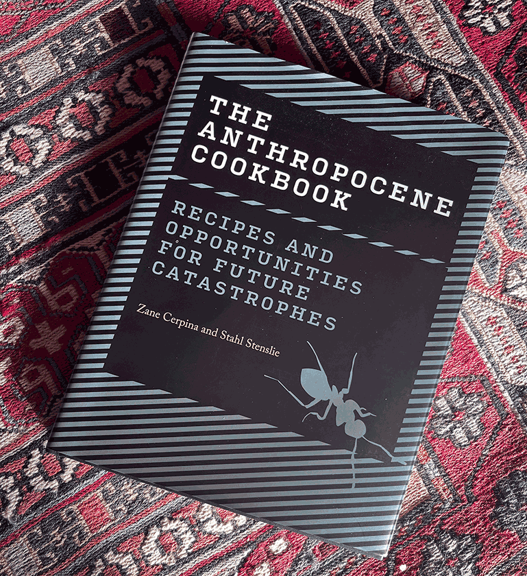
The Anthropocene Cookbook on October 16, 2023

[downloaded from: https://artscisalon.com/coms4208/]

From the Toronto ArtSci Salon October 5, 2023 announcement,

Oct 16 [2023], 3:30 PM [ET] 
The Anthropocene cookbook

with authors 
Zane Cerpina & Stahl Stenslie
Cerpina and Stenslie are the authors of
The Anthropocene Cookbook. How to survive in the age of catastrophes 

Join us to welcome Cerpina and Stenslie as they introduce us to their
book and discuss the future cuisine of humanity. To sustain the
soon-to-be 9 billion global population we cannot count on Mother
Earth’s resources anymore. The project explores innovative and
speculative ideas about new foods in the field of arts, design, science
& technology, rethinking eating traditions and food taboos, and
proposing new recipes for survival in times of ecological catastrophes.

To match the topic of their talk, attendees will be presented with
“anthropocene snacks” and will be encouraged to discuss food
alternatives and new networks of solidarity to fight food deserts,
waste, and unsustainable consumption.

This is a Hybrid event: our guests will join us virtually on zoom.
Join us in person at Glendon Campus, rm YH190 (the studio next to the
Glendon Theatre) for a more intimate community experience and some
anthropocene snacks. If you wish to join us on Zoom, please

register here

This event is part of a series on Emergent Practices in Communication,
featuring explorations on interspecies communication and digital
networks; land-based justice and collective care. The full program can be found here

This initiative is supported by York University’s Teaching Commons Academic Innovation Fund

Zane Cerpina is a multicultural and interdisciplinary female author,
curator, artist, and designer working with the complexity of
socio-political and environmental issues in contemporary society and in
the age of the Anthropocene. Cerpina earned her master’s degree in
design from AHO – The Oslo School of Architecture and Design and a
bachelor’s degree in Art and Technology from Aalborg University. She
resides in Oslo and is a project manager/curator at TEKS (Trondheim
Electronic Arts Centre). She is also a co-founder and editor of EE:
Experimental Emerging Art Journal. From 2015 to 2019, Cerpina was a
creative manager and editor at PNEK (Production Network for Electronic
Art, Norway).

Stahl Stenslie works as an artist, curator and researcher specializing
in experimental media art and interaction experiences. His aesthetic
focus is on art and artistic expressions that challenge ordinary ways of
perceiving the world. Through his practice he asks the questions we tend
to avoid – or where the answers lie in the shadows of existence.
Keywords of his practice are somaesthetics, unstable media,
transgression and numinousness. The technological focus in his works is
on the art of the recently possible – such as i) panhaptic
communication on Smartphones, ii) somatic and immersive soundspaces, and
iii) design of functional and lethal artguns, 3D printed in low-cost
plastic material.He has a PhD on Touch and Technologies from The School
of Architecture and Design, Oslo, Norway. Currently he heads the R&D
department at Arts for Young Audiences Norway.

If you’re interested in the book, there’s the anthropocenecookbook.com, which has more about the book and purchase information,

The Anthropocene Cookbook is by far the most comprehensive collection of ideas about future food from the perspective of art, design, and science. It is a thought-provoking book about art, food, and eating in the Anthropocene –The Age of Man– and the age of catastrophes.

Published by The MIT Press [MIT = Massachusetts Institute of Technology]
| mitpress.mit.edu

Supported by TEKS
Trondheim Electronic Arts Centre
| www.teks.no

*Date changed* Streaming Carbon Footprint on October 27, 2023

Keep scrolling down to Date & location changed for Streaming Carbon Footprint subhead.

From the Toronto ArtSci Salon October 5, 2023 announcement,

Oct 27, [2023] 5:00-7:00 PM  [ET]
Streaming Carbon Footprint

with 
Laura U. Marks
and
David Rokeby

Room 230
The Fields Institute for Research in Mathematical Sciences
222 College Street, Toronto

We are thrilled to announce this dialogue between media Theorist Laura U. Marks and Media Artist David Rokeby. Together, they will discuss a well known elephant in the room of media and digital technologies: their carbon footprint. As social media and streaming media usage increases exponentially, what can be done to mitigate their impact? are there alternatives?

This is a live event: our guests will join us in person.

if you wish to join us on Zoom instead, a link will be circulated on our website and on social media a few days before the event. The event will be recorded

Laura U. Marks works on media art and philosophy with an intercultural focus, and on small-footprint media. She programs experimental media for venues around the world. As Grant Strate University Professor, she teaches in the School for the Contemporary Arts at Simon Fraser University in Vancouver, Canada. Her upcoming book The Fold: From Your Body to the Cosmos will be published I March 2024 by Duke University Press. 

David Rokeby is an installation artist based in Toronto, Canada. He has been creating and exhibiting since 1982. For the first part of his career he focussed on interactive pieces that directly engage the human body, or that involve artificial perception systems. In the last decade, his practice has expanded to included video, kinetic and static sculpture. His work has been performed / exhibited in shows across Canada, the United States, Europe and Asia.

Awards include the first BAFTA (British Academy of Film and Television Arts) award for Interactive Art in 2000, a 2002 Governor General’s award in Visual and Media Arts and the Prix Ars Electronica Golden Nica for Interactive Art 2002. He was awarded the first Petro-Canada Award for Media Arts in 1988, the Prix Ars Electronica Award of Distinction for Interactive Art (Austria) in 1991 and 1997.

I haven’t been able to dig up any information about registration but it will be added here should I stumble across any in the next few weeks. I did, however, find more information about Marks’s work and a festival in Vancouver (Canada).

Fourth Annual Small File Media Festival (October 20 -21, 2023) and the Streaming Carbon Footprint

First, let’s flip back in time to a July 27, 2021 Simon Fraser University (SFU) news release (also published as a July 27, 2021 news item on phys.org) by Tessa Perkins Deneault,

When was the last time you watched a DVD? If you’re like most people, your DVD collection has been gathering dust as you stream movies and TV from a variety of on-demand services. But have you ever considered the impact of streaming video on the environment?

School for the Contemporary Arts professor Laura Marks and engineering professor Stephen Makonin, with engineering student Alejandro Rodriguez-Silva and media scholar Radek Przedpełski, worked together for over a year to investigate the carbon footprint of streaming media supported by a grant from the Social Sciences and Humanities Research Council of Canada.

“Stephen and Alejandro were there to give us a reality check and to increase our engineering literacy, and Radek and I brought the critical reading to it,” says Marks. “It was really a beautiful meeting of critical media studies and engineering.”

After combing through studies on Information and Communication Technologies (ICT) and making their own calculations, they confirmed that streaming media (including video on demand, YouTube, video embedded in social media and websites, video conferences, video calls and games) is responsible for more than one per cent of greenhouse gas emissions worldwide. And this number is only projected to rise as video conferencing and streaming proliferate.

“One per cent doesn’t sound like a lot, but it’s significant if you think that the airline industry is estimated to be 1.9 per cent,” says Marks. “ICT’s carbon footprint is growing fast, and I’m concerned that because we’re all turning our energy to other obvious carbon polluters, like fossil fuels, cars, the airline industry, people are not going to pay attention to this silent, invisible carbon polluter.”

One thing that Marks found surprising during their research is how politicized this topic is.

Their full report includes a section detailing the International Energy Association’s attack on French think tank The Shift Project after they published a report on streaming media’s carbon footprint in 2019. They found that some ICT engineers state that the carbon footprint of streaming is not a concern because data centres and networks are very efficient, while others say the fast-rising footprint is a serious problem that needs to be addressed. Their report includes comparisons of the divergent figures in engineering studies in order to get a better understanding of the scope of this problem.

The No. 1 thing Marks and Makonin recommend to reduce streaming’s carbon footprint is to ensure that our electricity comes from renewable sources. At an individual level, they offer a list of recommendations to reduce energy consumption and demand for new ICT infrastructure including: stream less, watch physical media including DVDs, decrease video resolution, use audio-only mode when possible, and keep your devices longer—since production of devices is very carbon-intensive.    

Promoting small files and low resolution, Marks founded the Small File Media Festival [link leads to 2023 programme], which will present its second annual program [2021] of 5-megabyte films Aug. 10 – 20. As the organizers say, movies don’t have to be big to be binge-worthy.

Learn more about Marks’ research and the Small File Media Festival: https://www.sfu.ca/sca/projects—activities/streaming-carbon-footprint.html

And now for 2023, here’s a video promoting the upcoming fourth annual festival,

The Streaming Carbon Footprint webpage on the SFU website includes information about the final report and the latest Small File Media Festival. Although I found the Small File Media Festival website also included a link for purchasing tickets,

The Small File Media Festival returns for its fourth iteration! We are delighted to partner with The Cinematheque to present over sixty jewel-like works from across the globe. These movies are small in file size, but huge in impact: by embracing the aesthetics of compression and low resolution (glitchiness, noise, pixelation), they lay the groundwork for a new experimental film movement in the digital age. This year, six lovingly curated programs traverse brooding pixelated landscapes, textural paradises, and crystalline infinities.

TICKETS AND FESTIVAL INFO

Join us Friday, October 20 [2023] for the opening-night program followed by a drinks reception in the lobby and a dance party in the cinema, featuring music by Vancouver electronic artist SAN. We’ll announce the winner of the coveted Small-File Golden Mini Bear during Saturday’s [October 21, 2023] award ceremony! As always, the festival will stream online at small​file​.ca after the live events.

We’re most grateful to our future-forward friends at the Social Sciences and Humanities Research Council of Canada, Canada Council for the Arts, and SFU Contemporary Arts. Thanks to VIVO Media Arts, Cairo Video Festival, and The Hmm for generous distribution and exhibition awards, and to UKRAïNATV, a partner in small-file activism.

Cosmically healthy, community-building, and punk AF, small-file ecomedia will heal the world, one pixel at a time.

TICKETS

There we have it. And then, we didn’t

*Date & location change* for Streaming Carbon Footprint event

From an October 27, 2023 ArtSci Salon notice,

Nov 7, [2023] 5:00-7:00 PM 
Streaming Carbon Footprint

with 
Laura U. Marks
and
David Rokeby
 

Tuesday, November 7 [2023]
5:00-7:00 pm
The BMO Lab
15 King’s College Circle, room H-12
Toronto, Ontario M5S 3H7

Good luck to the organizers. It must have been nervewracking to change the date so late in the game.

IBM’s neuromorphic chip, a prototype and more

it seems IBM is very excited about neuromorphic computing. First, there’s an August 10, 2023 news article by Shiona McCallum & Chris Vallance for British Broadcasting Corporation (BBC) online news,

Concerns have been raised about emissions associated with warehouses full of computers powering AI systems.

IBM said its prototype could lead to more efficient, less battery draining AI chips for smartphones.

Its efficiency is down to components that work in a similar way to connections in human brains, it said.

Compared to traditional computers, “the human brain is able to achieve remarkable performance while consuming little power”, said scientist Thanos Vasilopoulos, based at IBM’s research lab in Zurich, Switzerland.

I sense a memristor about to be mentioned, from McCallum & Vallance’s article August 10, 2023 news article,

Most chips are digital, meaning they store information as 0s and 1s, but the new chip uses components called memristors [memory resistors] that are analogue and can store a range of numbers.

You can think of the difference between digital and analogue as like the difference between a light switch and a dimmer switch.

The human brain is analogue, and the way memristors work is similar to the way synapses in the brain work.

Prof Ferrante Neri, from the University of Surrey, explains that memristors fall into the realm of what you might call nature-inspired computing that mimics brain function.

A memristor could “remember” its electric history, in a similar way to a synapse in a biological system.

“Interconnected memristors can form a network resembling a biological brain,” he said.

He was cautiously optimistic about the future for chips using this technology: “These advancements suggest that we may be on the cusp of witnessing the emergence of brain-like chips in the near future.”

However, he warned that developing a memristor-based computer is not a simple task and that there would be a number of challenges ahead for widespread adoption, including the costs of materials and manufacturing difficulties.

Neri is most likely aware that researchers have been excited that ‘green’ computing could be made possible by memristors since at least 2008 (see my May 9, 2008 posting “Memristors and green energy“).

As it turns out, IBM published two studies on neuromorphic chips in August 2023.

The first study (mentioned in the BBC article) is also described in an August 22, 2023 article by Peter Grad for Tech Xpore. This one is a little more technical than the BBC article,

For those who are truly technical, here’s a link to and a citation for the paper,

A 64-core mixed-signal in-memory compute chip based on phase-change memory for deep neural network inference by Manuel Le Gallo, Riduan Khaddam-Aljameh, Milos Stanisavljevic, Athanasios Vasilopoulos, Benedikt Kersting, Martino Dazzi, Geethan Karunaratne, Matthias Brändli, Abhairaj Singh, Silvia M. Müller, Julian Büchel, Xavier Timoneda, Vinay Joshi, Malte J. Rasch, Urs Egger, Angelo Garofalo, Anastasios Petropoulos, Theodore Antonakopoulos, Kevin Brew, Samuel Choi, Injo Ok, Timothy Philip, Victor Chan, Claire Silvestre, Ishtiaq Ahsan, Nicole Saulnier, Nicole Saulnier, Pier Andrea Francese, Evangelos Eleftheriou & Abu Sebastian. Nature Electronics (2023) DOI: https://doi.org/10.1038/s41928-023-01010-1 Published: 10 August 2023

This paper is behind a paywall.

Before getting to the second paper, there’s an August 23, 2023 IBM blog post by Mike Murphy announcing its publication in Nature, Note: Links have been removed,

Although we’re still just at the precipice of the AI revolution, artificial intelligence has already begun to revolutionize the way we live and work. There’s just one problem: AI technology is incredibly power-hungry. By some estimates, running a large AI model generates more emissions over its lifetime than the average American car.

The future of AI requires new innovations in energy efficiency, from the way models are designed down to the hardware that runs them. And in a world that’s increasingly threatened by climate change, any advances in AI energy efficiency are essential to keep pace with AI’s rapidly expanding carbon footprint.

And one of the latest breakthroughs in AI efficiency from IBM Research relies on analog chips — ones that consume much less power. In a paper published in Nature today,1 researchers from IBM labs around the world presented their prototype analog AI chip for energy-efficient speech recognition and transcription. Their design was utilized in two AI inference experiments, and in both cases, the analog chips performed these tasks just as reliably as comparable all-digital devices — but finished the tasks faster and used less energy.

The concept of designing analog chips for AI inference is not new — researchers have been contemplating the idea for years. Back in 2021, a team at IBM developed chips that use Phase-change memory (PCM) works when an electrical pulse is applied to a material, which changes the conductance of the device. The material switches between amorphous and crystalline phases, where a lower electrical pulse will make the device more crystalline, providing less resistance, and a high enough electrical pulse makes the device amorphous, resulting in large resistance. Instead of recording the usual 0s or 1s you would see in digital systems, the PCM device records its state as a continuum of values between the amorphous and crystalline states. This value is called a synaptic weight, which can be stored in the physical atomic configuration of each PCM device. The memory is non-volatile, so the weights are retained when the power supply is switched off.phase-change memory to encode the weights of a neural network directly onto the physical chip. But previous research in the field hasn’t shown how chips like these could be used on the massive models we see dominating the AI landscape today. For example, GPT-3, one of the larger popular models, has 175 billion parameters, or weights.

Murphy also explains the difference (for amateurs like me) between this work and the earlier published study, from the August 23, 2023 IBM blog post, Note: Links have been removed,

Natural-language tasks aren’t the only AI problems that analog AI could solve — IBM researchers are working on a host of other uses. In a paper published earlier this month in Nature Electronics, the team showed it was possible to use an energy-efficient analog chip design for scalable mixed-signal architecture that can achieve high accuracy in the CIFAR-10 image dataset for computer vision image recognition.

These chips were conceived and designed by IBM researchers in the Tokyo, Zurich, Yorktown Heights, New York, and Almaden, California labs, and built by an external fabrication company. The phase change memory and metal levels were processed and validated at IBM Research’s lab in the Albany Nanotech Complex.

If you were to combine the benefits of the work published today in Nature, such as large arrays and parallel data-transport, with the capable digital compute-blocks of the chip shown in the Nature Electronics paper, you would see many of the building blocks needed to realize the vision of a fast, low-power analog AI inference accelerator. And pairing these designs with hardware-resilient training algorithms, the team expects these AI devices to deliver the software equivalent of neural network accuracies for a wide range of AI models in the future.

Here’s a link to and a citation for the second paper,

An analog-AI chip for energy-efficient speech recognition and transcription by S. Ambrogio, P. Narayanan, A. Okazaki, A. Fasoli, C. Mackin, K. Hosokawa, A. Nomura, T. Yasuda, A. Chen, A. Friz, M. Ishii, J. Luquin, Y. Kohda, N. Saulnier, K. Brew, S. Choi, I. Ok, T. Philip, V. Chan, C. Silvestre, I. Ahsan, V. Narayanan, H. Tsai & G. W. Burr. Nature volume 620, pages 768–775 (2023) DOI: https://doi.org/10.1038/s41586-023-06337-5 Published: 23 August 2023 Issue Date: 24 August 2023

This paper is open access.

10 years of the European Union’s roll of the dice: €1B or 1billion euros each for the Human Brain Project (HBP) and the Graphene Flagship

Graphene and Human Brain Project win biggest research award in history (& this is the 2000th post)” on January 28, 2013 was how I announced the results of what had been a a European Union (EU) competition that stretched out over several years and many stages as projects were evaluated and fell to the wayside or were allowed onto the next stage. The two finalists received €1B each to be paid out over ten years.

Human Brain Project (HBP)

A September 12, 2023 Human Brain Project (HBP) press release (also on EurekAlert) summarizes the ten year research effort and the achievements,

The EU-funded Human Brain Project (HBP) comes to an end in September and celebrates its successful conclusion today with a scientific symposium at Forschungszentrum Jülich (FZJ). The HBP was one of the first flagship projects and, with 155 cooperating institutions from 19 countries and a total budget of 607 million euros, one of the largest research projects in Europe. Forschungszentrum Jülich, with its world-leading brain research institute and the Jülich Supercomputing Centre, played an important role in the ten-year project.

“Understanding the complexity of the human brain and explaining its functionality are major challenges of brain research today”, says Astrid Lambrecht, Chair of the Board of Directors of Forschungszentrum Jülich. “The instruments of brain research have developed considerably in the last ten years. The Human Brain Project has been instrumental in driving this development – and not only gained new insights for brain research, but also provided important impulses for information technologies.”

HBP researchers have employed highly advanced methods from computing, neuroinformatics and artificial intelligence in a truly integrative approach to understanding the brain as a multi-level system. The project has contributed to a deeper understanding of the complex structure and function of the brain and enabled novel applications in medicine and technological advances.

Among the project’s highlight achievements are a three-dimensional, digital atlas of the human brain with unprecedented detail, personalised virtual models of patient brains with conditions like epilepsy and Parkinson’s, breakthroughs in the field of artificial intelligence, and an open digital research infrastructure – EBRAINS – that will remain an invaluable resource for the entire neuroscience community beyond the end of the HBP.

Researchers at the HBP have presented scientific results in over 3000 publications, as well as advanced medical and technical applications and over 160 freely accessible digital tools for neuroscience research.

“The Human Brain Project has a pioneering role for digital brain research with a unique interdisciplinary approach at the interface of neuroscience, computing and technology,” says Katrin Amunts, Director of the HBP and of the Institute for Neuroscience and Medicine at FZJ. “EBRAINS will continue to power this new way of investigating the brain and foster developments in brain medicine.”

“The impact of what you achieved in digital science goes beyond the neuroscientific community”, said Gustav Kalbe, CNECT, Acting Director of Digital Excellence and Science Infrastructures at the European Commission during the opening of the event. “The infrastructure that the Human Brain Project has established is already seen as a key building block to facilitate cooperation and research across geographical boundaries, but also across communities.”

Further information about the Human Brain Project as well as photos from research can be found here: https://fz-juelich.sciebo.de/s/hWJkNCC1Hi1PdQ5.

Results highlights and event photos in the online press release.

Results overviews:
– “Human Brain Project: Spotlights on major achievements” and “A closer Look on Scientific
Advances”

– “Human Brain Project: An extensive guide to the tools developed”

Examples of results from the Human Brain Project:

As the “Google Maps of the brain” [emphasis mine], the Human Brain Project makes the most comprehensive digital brain atlas to date available to all researchers worldwide. The atlas by Jülich researchers and collaborators combines high-resolution data of neurons, fibre connections, receptors and functional specialisations in the brain, and is designed as a constantly growing system.

13 hospitals in France are currently testing the new “Virtual Epileptic Patient” – a platform developed at the University of Marseille [Aix-Marseille University?] in the Human Brain Project. It creates personalised simulation models of brain dynamics to provide surgeons with predictions for the success of different surgical treatment strategies. The approach was presented this year in the journals Science Translational Medicine and The Lancet Neurology.


SpiNNaker2 is a “neuromorphic” [brainlike] computer developed by the University of Manchester and TU Dresden within the Human Brain Project. The company SpiNNcloud Systems in Dresden is commercialising the approach for AI applications. (Image: Sprind.org)

As an openly accessible digital infrastructure, EBRAINS offers scientists easy access to the best techniques for complex research questions.

[https://www.ebrains.eu/]

There was a Canadian connection at one time; Montréal Neuro at Canada’s McGill University was involved in developing a computational platform for neuroscience (CBRAIN) for HBP according to an announcement in my January 29, 2013 posting. However, there’s no mention of the EU project on the CBRAIN website nor is there mention of a Canadian partner on the EBRAINS website, which seemed the most likely successor to the CBRAIN portion of the HBP project originally mentioned in 2013.

I couldn’t resist “Google maps of the brain.”

In any event, the statement from Astrid Lambrecht offers an interesting contrast to that offered by the leader of the other project.

Graphene Flagship

In fact, the Graphene Flagship has been celebrating its 10th anniversary since last year; see my September 1, 2022 posting titled “Graphene Week (September 5 – 9, 2022) is a celebration of 10 years of the Graphene Flagship.”

The flagship’s lead institution, Chalmers University of Technology in Sweden, issued an August 28, 2023 press release by Lisa Gahnertz (also on the Graphene Flagship website but published September 4, 2023) touting its achievement with an ebullience I am more accustomed to seeing in US news releases,

Chalmers steers Europe’s major graphene venture to success

For the past decade, the Graphene Flagship, the EU’s largest ever research programme, has been coordinated from Chalmers with Jari Kinaret at the helm. As the project reaches the ten-year mark, expectations have been realised, a strong European research field on graphene has been established, and the journey will continue.

‘Have we delivered what we promised?’ asks Graphene Flagship Director Jari Kinaret from his office in the physics department at Chalmers, overlooking the skyline of central Gothenburg.

‘Yes, we have delivered more than anyone had a right to expect,’ [emphasis mine] he says. ‘In our analysis for the conclusion of the project, we read the documents that were written at the start. What we promised then were over a hundred specific things. Some of them were scientific and technological promises, and they have all been fulfilled. Others were for specific applications, and here 60–70 per cent of what was promised has been delivered. We have also delivered applications we did not promise from the start, but these are more difficult to quantify.’

The autumn of 2013 saw the launch of the massive ten-year Science, Technology and Innovation research programme on graphene and other related two-dimensional materials. Joint funding from the European Commission and EU Member States totalled a staggering €1,000 million. A decade later, it is clear that the large-scale initiative has succeeded in its endeavours. According to a report by the research institute WifOR, the Graphene Flagship will have created a total contribution to GDP of €3,800 million and 38,400 new jobs in the 27 EU countries between 2014 and 2030.

Exceeded expectations

‘Per euro invested and compared to other EU projects, the flagship has performed 13 times better than expected in terms of patent applications, and seven times better for scientific publications. We have 17 spin-off companies that have received over €130 million in private funding – people investing their own money is a real example of trust in the fact that the technology works,’ says Jari Kinaret.

He emphasises that the long time span has been crucial in developing the concepts of the various flagship projects.

‘When it comes to new projects, the ability to work on a long timescale is a must and is more important than a large budget. It takes a long time to build trust, both in one another within a team and in the technology on the part of investors, industry and the wider community. The size of the project has also been significant. There has been an ecosystem around the material, with many graphene manufacturers and other organisations involved. It builds robustness, which means you have the courage to invest in the material and develop it.’

From lab to application

In 2010, Andre Geim and Konstantin Novoselov of the University of Manchester won the Nobel Prize in Physics for their pioneering experiments isolating the ultra-light and ultra-thin material graphene. It was the first known 2D material and stunned the world with its ‘exceptional properties originating in the strange world of quantum physics’ according to the Nobel Foundation’s press release. Many potential applications were identified for this electrically conductive, heat-resistant and light-transmitting material. Jari Kinaret’s research team had been exploring the material since 2006, and when Kinaret learned of the European Commission’s call for a ten-year research programme, it prompted him to submit an application. The Graphene Flagship was initiated to ensure that Europe would maintain its leading position in graphene research and innovation, and its coordination and administration fell to Chalmers.

Is it a staggering thought that your initiative became the biggest EU research project of all time?

‘The fact that the three-minute presentation I gave at a meeting in Brussels has grown into an activity in 22 countries, with 170 organisations and 1,300 people involved … You can’t think about things like that because it can easily become overwhelming. Sometimes you just have to go for it,’ says Jari Kinaret.

One of the objectives of the Graphene Flagship was to take the hopes for this material and move them from lab to application. What has happened so far?

‘We are well on track with 100 products priced and on their way to the market. Many of them are business-to-business products that are not something we ordinary consumers are going to buy, but which may affect us indirectly.’

‘It’s important to remember that getting products to the application stage is a complex process. For a researcher, it may take ten working prototypes; for industry, ten million. Everything has to click into place, on a large scale. All components must work identically and in exactly the same way, and be compatible with existing production in manufacturing as you cannot rebuild an entire factory for a new material. In short, it requires reliability, reproducibility and manufacturability.’

Applications in a wide range of areas

Graphene’s extraordinary properties are being used to deliver the next generation of technologies in a wide range of fields, such as sensors for self-driving cars, advanced batteries, new water purification methods and sophisticated instruments for use in neuroscience. When asked if there are any applications that Jani Kinaret himself would like to highlight, he mentions, among other things, the applications that are underway in the automotive industry – such as sensors to detect obstacles for self-driving cars. Thanks to graphene, they will be so cost-effective to produce that it will be possible to make them available in more than just the most expensive car models.

He also highlights the aerospace industry, where a graphene material for removing ice from aircraft and helicopter wings is under development for the Airbus company. Another favourite, which he has followed from basic research to application, is the development of an air cleaner for Lufthansa passenger aircraft, based on a kind of ‘graphene foam’. Because graphene foam is very light, it can be heated extremely quickly. A pulse of electricity lasting one thousandth of a second is enough to raise the temperature to 300 degrees, thus killing micro-organisms and effectively cleaning the air in the aircraft.

He also mentions the Swedish company ABB, which has developed a graphene composite for circuit breakers in switchgear. These circuit breakers are used to protect the electricity network and must be safe to use. The graphene composite replaces the manual lubrication of the circuit breakers, resulting in significant cost savings.

‘We also see graphene being used in medical technology, but its application requires many years of testing and approval by various bodies. For example, graphene technology can more effectively map the brain before neurosurgery, as it provides a more detailed image. Another aspect of graphene is that it is soft and pliable. This means it can be used for electrodes that are implanted in the brain to treat tremors in Parkinson’s patients, without the electrodes causing scarring,’ says Jari Kinaret.

Coordinated by Chalmers

Jari Kinaret sees the fact that the EU chose Chalmers as the coordinating university as a favourable factor for the Graphene Flagship.

‘Hundreds of millions of SEK [Swedish Kroner] have gone into Chalmers research, but what has perhaps been more important is that we have become well-known and visible in certain areas. We also have the 2D-Tech competence centre and the SIO Grafen programme, both funded by Vinnova and coordinated by Chalmers and Chalmers industriteknik respectively. I think it is excellent that Chalmers was selected, as there could have been too much focus on the coordinating organisation if it had been more firmly established in graphene research at the outset.’

What challenges have been encountered during the project?

‘With so many stakeholders involved, we are not always in agreement. But that is a good thing. A management book I once read said that if two parties always agree, then one is redundant. At the start of the project, it was also interesting to see the major cultural differences we had in our communications and that different cultures read different things between the lines; it took time to realise that we should be brutally straightforward in our communications with one another.’

What has it been like to have the coordinating role that you have had?

‘Obviously, I’ve had to worry about things an ordinary physics professor doesn’t have to worry about, like a phone call at four in the morning after the Brexit vote or helping various parties with intellectual property rights. I have read more legal contracts than I thought I would ever have to read as a professor. As a researcher, your approach when you go into a role is narrow and deep, here it was rather all about breadth. I would have liked to have both, but there are only 26 hours in a day,’ jokes Jari Kinaret.

New phase for the project and EU jobs to come

A new assignment now awaits Jari Kinaret outside Chalmers as Chief Executive Officer of the EU initiative KDT JU (Key Digital Technologies Joint Undertaking, soon to become Chips JU), where industry and the public sector interact to drive the development of new electronic components and systems.

The Graphene Flagship may have reached its destination in its current form, but the work started is progressing in a form more akin to a flotilla. About a dozen projects will continue to live on under the auspices of the European Commission’s Horizon Europe programme. Chalmers is going to coordinate a smaller CSA project called GrapheneEU, where CSA stands for ‘Coordination and Support Action’. It will act as a cohesive force between the research and innovation projects that make up the next phase of the flagship, offering them a range of support and services, including communication, innovation and standardisation.

The Graphene Flagship is about to turn ten. If the project had been a ten-year-old child, what kind of child would it have been?

‘It would have been a very diverse organism. Different aspirations are beginning to emerge – perhaps it is adolescence that is approaching. In addition, within the project we have also studied other related 2D materials, and we found that there are 6,000 distinct materials of this type, of which only about 100 have been studied. So, it’s the younger siblings that are starting to arrive now.’

Facts about the Graphene Flagship:

The Graphene Flagship is the first European flagship for future and emerging technologies. It has been coordinated and administered from the Department of Physics at Chalmers, and as the project enters its next phase, GrapheneEU, coordination will continue to be carried out by staff currently working on the flagship led by Chalmers Professor Patrik Johansson.

The project has proved highly successful in developing graphene-based technology in Europe, resulting in 17 new companies, around 100 new products, nearly 500 patent applications and thousands of scientific papers. All in all, the project has exceeded the EU’s targets for utilisation from research projects by a factor of ten. According to the assessment of the EU research programme Horizon 2020, Chalmers’ coordination of the flagship has been identified as one of the key factors behind its success.

Graphene Week will be held at the Svenska Mässan in Gothenburg from 4 to 8 September 2023. Graphene Week is an international conference, which also marks the finale of the ten-year anniversary of the Graphene Flagship. The conference will be jointly led by academia and industry – Professor Patrik Johansson from Chalmers and Dr Anna Andersson from ABB – and is expected to attract over 400 researchers from Sweden, Europe and the rest of the world. The programme includes an exhibition, press conference and media activities, special sessions on innovation, diversity and ethics, and several technical sessions. The full programme is available here.

Read the press release on Graphene Week from 4 to 8 September and the overall results of the Graphene Flagship. …

Ten years and €1B each. Congratulations to the organizers on such massive undertakings. As for whether or not (and how they’ve been successful), I imagine time will tell.

Sign up for Nano4EARTH’s Roundtable Discussion (Batteries and Energy Storage): September 26, 2023 (online or in person)

Given that Nano4Earth was first announced by the US government in October 2022 (see my November 28, 2022 posting), the initiative has been quite active (see my February 27, 2023 posting, “Nano4EARTH workshop recordings available online“).

Now for the latest, from the National Nanotechnology Initiative (NNI) webpage for the batteries and storage roundtable discussion,

Nano4EARTH Roundtable Discussion on Batteries and Energy Storage

September 26, 2023
9:30 a.m. to 3:30 p.m. ET
Online and L’Enfant Plaza SW, Washington, D.C.

The Nano4EARTH roundtable discussion on batteries and energy storage aims to identify fundamental knowledge gaps, needs, and opportunities to advance current electrification goals. By convening stakeholders from different sectors, backgrounds, and expertise the goal of this roundtable is to identify applicable lessons across the spectrum of technologies, discuss system-specific needs, scalability and commercialization challenges, and potential paths forward. These needs could have a near-term impact on energy efficiency, sustainable development, and climate change. The moderated discussion will tackle all aspects of the topic – ranging from exciting R&D opportunities to commercialization challenges – by featuring a small group of experts from different sectors and backgrounds.

This roundtable is a critical part of the Nano4EARTH National Nanotechnology Challenge, which aims to leverage recent investments in understanding and controlling matter at the nanoscale to develop technologies and industries that address climate change. Nano4EARTH focuses on facilitating opportunities for members of the nanotechnology community to convene, collaborate, and share resources. Nano4EARTH also strives to provide mechanisms that support technology development and commercialization of nanotechnology-enabled climate solutions.

The topic of this roundtable was identified at the Nano4EARTH kick-off workshop (summary readout and video archive) as a particularly promising area that could have an impact in a short time frame (four years or less). This roundtable is the second of four.

MEETING LOCATION:

Online and the National Nanotechnology Coordination Office: Suite 8001, 470 L’Enfant Plaza SW, Washington, DC 20024. Directions are available here.

Registration is now open and you can find the links to online or in person registration on the National Nanotechnology Initiative (NNI) webpage for the batteries and storage roundtable discussion

h/t JD Supra blog’s August 23, 2023 posting

Single chip mimics human vision and memory abilities

A June 15, 2023 RMIT University (Australia) press release (also on EurekAlert but published June 14, 2023) announces a neuromorphic (brainlike) computer chip, which mimics human vision and ‘creates’ memories,

Researchers have created a small device that ‘sees’ and creates memories in a similar way to humans, in a promising step towards one day having applications that can make rapid, complex decisions such as in self-driving cars.

The neuromorphic invention is a single chip enabled by a sensing element, doped indium oxide, that’s thousands of times thinner than a human hair and requires no external parts to operate.

RMIT University engineers in Australia led the work, with contributions from researchers at Deakin University and the University of Melbourne.

The team’s research demonstrates a working device that captures, processes and stores visual information. With precise engineering of the doped indium oxide, the device mimics a human eye’s ability to capture light, pre-packages and transmits information like an optical nerve, and stores and classifies it in a memory system like the way our brains can.

Collectively, these functions could enable ultra-fast decision making, the team says.

Team leader Professor Sumeet Walia said the new device can perform all necessary functions – sensing, creating and processing information, and retaining memories – rather than relying on external energy-intensive computation, which prevents real-time decision making.

“Performing all of these functions on one small device had proven to be a big challenge until now,” said Walia from RMIT’s School of Engineering.

“We’ve made real-time decision making a possibility with our invention, because it doesn’t need to process large amounts of irrelevant data and it’s not being slowed down by data transfer to separate processors.”

What did the team achieve and how does the technology work?

The new device was able to demonstrate an ability to retain information for longer periods of time, compared to previously reported devices, without the need for frequent electrical signals to refresh the memory. This ability significantly reduces energy consumption and enhances the device’s performance.

Their findings and analysis are published in Advanced Functional Materials.

First author and RMIT PhD researcher Aishani Mazumder said the human brain used analog processing, which allowed it to process information quickly and efficiently using minimal energy.

“By contrast, digital processing is energy and carbon intensive, and inhibits rapid information gathering and processing,” she said.

“Neuromorphic vision systems are designed to use similar analog processing to the human brain, which can greatly reduce the amount of energy needed to perform complex visual tasks compared with today’s technologies

What are the potential applications?

The team used ultraviolet light as part of their experiments, and are working to expand this technology even further for visible and infrared light – with many possible applications such as bionic vision, autonomous operations in dangerous environments, shelf-life assessments of food and advanced forensics.

“Imagine a self-driving car that can see and recognise objects on the road in the same way that a human driver can or being able to able to rapidly detect and track space junk. This would be possible with neuromorphic vision technology.”

Walia said neuromorphic systems could adapt to new situations over time, becoming more efficient with more experience.

“Traditional computer vision systems – which cannot be miniaturised like neuromorphic technology – are typically programmed with specific rules and can’t adapt as easily,” he said.

“Neuromorphic robots have the potential to run autonomously for long periods, in dangerous situations where workers are exposed to possible cave-ins, explosions and toxic air.”

The human eye has a single retina that captures an entire image, which is then processed by the brain to identify objects, colours and other visual features.

The team’s device mimicked the retina’s capabilities by using single-element image sensors that capture, store and process visual information on one platform, Walia said.

“The human eye is exceptionally adept at responding to changes in the surrounding environment in a faster and much more efficient way than cameras and computers currently can,” he said.

“Taking inspiration from the eye, we have been working for several years on creating a camera that possesses similar abilities, through the process of neuromorphic engineering.” 

Here’s a link to and a citation for the paper,

Long Duration Persistent Photocurrent in 3 nm Thin Doped Indium Oxide for Integrated Light Sensing and In-Sensor Neuromorphic Computation by Aishani Mazumder, Chung Kim Nguyen, Thiha Aung, Mei Xian Low, Md. Ataur Rahman, Salvy P. Russo, Sherif Abdulkader Tawfik, Shifan Wang, James Bullock, Vaishnavi Krishnamurthi. Advanced Functional Materials DOI: https://doi.org/10.1002/adfm.202303641 First published: 14 June 2023

This paper is open access.

Optical memristors and neuromorphic computing

A June 5, 2023 news item on Nanowerk announced a paper which reviews the state-of-the-art of optical memristors, Note: Links have been removed,

AI, machine learning, and ChatGPT may be relatively new buzzwords in the public domain, but developing a computer that functions like the human brain and nervous system – both hardware and software combined – has been a decades-long challenge. Engineers at the University of Pittsburgh are today exploring how optical “memristors” may be a key to developing neuromorphic computing.

Resistors with memory, or memristors, have already demonstrated their versatility in electronics, with applications as computational circuit elements in neuromorphic computing and compact memory elements in high-density data storage. Their unique design has paved the way for in-memory computing and captured significant interest from scientists and engineers alike.

A new review article published in Nature Photonics (“Integrated Optical Memristors”), sheds light on the evolution of this technology—and the work that still needs to be done for it to reach its full potential. Led by Nathan Youngblood, assistant professor of electrical and computer engineering at the University of Pittsburgh Swanson School of Engineering, the article explores the potential of optical devices which are analogs of electronic memristors. This new class of device could play a major role in revolutionizing high-bandwidth neuromorphic computing, machine learning hardware, and artificial intelligence in the optical domain.

A June 2, 2023 University of Pittsburgh news release (also on EurekAlert but published June 5, 2023), which originated the news item, provides more detail,

“Researchers are truly captivated by optical memristors because of their incredible potential in high-bandwidth neuromorphic computing, machine learning hardware, and artificial intelligence,” explained Youngblood. “Imagine merging the incredible advantages of optics with local information processing. It’s like opening the door to a whole new realm of technological possibilities that were previously unimaginable.” 

The review article presents a comprehensive overview of recent progress in this emerging field of photonic integrated circuits. It explores the current state-of-the-art and highlights the potential applications of optical memristors, which combine the benefits of ultrafast, high-bandwidth optical communication with local information processing. However, scalability emerged as the most pressing issue that future research should address. 

“Scaling up in-memory or neuromorphic computing in the optical domain is a huge challenge. Having a technology that is fast, compact, and efficient makes scaling more achievable and would represent a huge step forward,” explained Youngblood. 

“One example of the limitations is that if you were to take phase change materials, which currently have the highest storage density for optical memory, and try to implement a relatively simplistic neural network on-chip, it would take a wafer the size of a laptop to fit all the memory cells needed,” he continued. “Size matters for photonics, and we need to find a way to improve the storage density, energy efficiency, and programming speed to do useful computing at useful scales.”

Using Light to Revolutionize Computing

Optical memristors can revolutionize computing and information processing across several applications. They can enable active trimming of photonic integrated circuits (PICs), allowing for on-chip optical systems to be adjusted and reprogrammed as needed without continuously consuming power. They also offer high-speed data storage and retrieval, promising to accelerate processing, reduce energy consumption, and enable parallel processing. 

Optical memristors can even be used for artificial synapses and brain-inspired architectures. Dynamic memristors with nonvolatile storage and nonlinear output replicate the long-term plasticity of synapses in the brain and pave the way for spiking integrate-and-fire computing architectures.

Research to scale up and improve optical memristor technology could unlock unprecedented possibilities for high-bandwidth neuromorphic computing, machine learning hardware, and artificial intelligence. 

“We looked at a lot of different technologies. The thing we noticed is that we’re still far away from the target of an ideal optical memristor–something that is compact, efficient, fast, and changes the optical properties in a significant manner,” Youngblood said. “We’re still searching for a material or a device that actually meets all these criteria in a single technology in order for it to drive the field forward.”

The publication of “Integrated Optical Memristors” (DOI: 10.1038/s41566-023-01217-w) was published in Nature Photonics and is coauthored by senior author Harish Bhaskaran at the University of Oxford, Wolfram Pernice at Heidelberg University, and Carlos Ríos at the University of Maryland.

Despite including that final paragraph, I’m also providing a link to and a citation for the paper,

Integrated optical memristors by Nathan Youngblood, Carlos A. Ríos Ocampo, Wolfram H. P. Pernice & Harish Bhaskaran. Nature Photonics volume 17, pages 561–572 (2023) DOI: https://doi.org/10.1038/s41566-023-01217-w Published online: 29 May 2023 Issue Date: July 2023

This paper is behind a paywall.

Wearable screen (flexible display) from the University of British Columbia (UBC)

If I read this correctly, the big selling point for UBC’s flexible, wearable display screen is energy efficiency. From a July 10, 2023 University of British Columbia (UBC) news release on EurekAlert,

Imagine a wearable patch that tracks your vital signs through changes in the colour display, or shipping labels that light up to indicate changes in temperature or sterility of food items.

These are among the potential uses for a new flexible display created by UBC researchers and announced recently in ACS Applied Materials and Interfaces.

“This device is capable of fast, realtime and reversible colour change,” says researcher Claire Preston, who developed the device as part of her master’s in electrical and computer engineering at UBC. “It can stretch up to 30 per cent without losing performance. It uses a colour-changing technology that can be used for visual monitoring. And it is relatively cheap to manufacture.”

Previous attempts at creating stretchable displays have involved complex designs and materials, limiting their stretchability and optical quality. In this new research, scientists leaned on electrochromic displays—which are able to reversibly change colour, while requiring low power consumption—to overcome these limitations. [emphasis mine]

“We used PEDOT:PSS, an electrochromic material that consists of a conductive polymer combined with an ionic liquid, resulting in a stretchable electrode that acts as both the electrochromic element and the ion storage layer. This simplifies the device’s architecture and eliminates the need for a separate stretchable conductor,” says Ms. Preston.

The display is transparent and feels like a stiff rubber band. To support the thin layers of PEDOT and allow them to elongate without breaking, the team added a solid polymer electrolyte and a stretchable encapsulation material called styrene-ethylene-butylene-styrene (SEBS).

“The potential uses for this stretchable display are significant. It could be integrated into wearable devices for biometric monitoring, allowing for real-time visual feedback on vital signs. The displays could also be used in robotic skin, enabling robots to display information and interact more intuitively with humans,” noted senior author Dr. John Madden, a professor of electrical and computer engineering who supervised the work.

Additionally, the low power consumption and cost-effectiveness of this technology make it attractive for use in disposable applications such as indicator patches for medical purposes or smart packaging labels for sensitive shipments. It could also be used to actively change the colour of jackets, hats and other garments.

“While there is need for more work to integrate this device into everyday devices, this breakthrough brings us one step closer to a future where flexible and stretchable displays are a common part of our daily lives,” Dr. Madden added.

Here’s a link to and a citation for the paper,

Intrinsically Stretchable Integrated Passive Matrix Electrochromic Display Using PEDOT:PSS Ionic Liquid Composite by Claire Preston, Yuta Dobashi, Ngoc Tan Nguyen, Mirza Saquib Sarwar, Daniel Jun, Cédric Plesse, Xavier Sallenave, Frédéric Vidal, Pierre-Henri Aubert, and John D. W. Madden. ACS Appl. Mater. Interfaces 2023, 15, 23, 28288–28299 DOI: https://doi.org/10.1021/acsami.3c02902 Publication Date: June 5, 2023 Copyright © 2023 The Authors. Published by American Chemical Society

This paper is open access.

Organic-inorganic nanohybrids: organic ligands attached to colloidal inorganic nanocrystals

A May 24, 2023 news item on phys.org introduces organic-inorganic nanohybrids for optoelectronic devices,

When designing optoelectronic devices, such as solar cells, photocatalysts, and photodetectors, scientists usually prioritize materials that are stable and possess tunable properties. This allows them precise control over optical characteristics of the materials and ensures retention of their properties over time, despite varying environmental conditions.

Organic-inorganic nanohybrids, which are made up of organic ligands attached to the surface of colloidal inorganic nanocrystals via coordinate bonds, are promising in this regard. They are known to exhibit enhanced stability owing to the formation of a protective layer by organic ligands around the reactive inorganic nanocrystal. However, the incorporation of organic ligands has been found to lower the conductivity and photon absorption efficiency of inorganic nanocrystals.

In a breakthrough study on ligand-nanocrystal interactions, researchers from Japan now demonstrate a quasi-reversible displacement of organic ligands on the surface of nanocrystals. Their findings, published in ACS Nano, provide a new perspective to the common belief that the organic ligands are anchored to the surface of the nanocrystals.

A May 22, 2023 Ritsumeikan University (Japan) press release (also on EurekAlert but published May 24, 2023), which originated the news item, provides more detail,

… The research team, led by Professor Yoichi Kobayashi from Ritsumeikan University, Japan, found that the coordination bond between perylene bisimide with a carboxyl group (PBI) and inorganic zinc sulfide (ZnS) nanocrystals can be reversibly displaced by exposing the material to visible light.

Shedding light on this novel behavior of organic-inorganic nanohybrids, Prof. Kobayashi says, “We explored the ligand properties of organic-inorganic nanohybrid systems by using perylene bisimide with a carboxyl group (PBI)-coordinated zinc sulfide (ZnS) NCs (PBI–ZnS) as a model system. Our findings provide the first example of photoinduced displacement of aromatic ligands with semiconductor nanocrystals.”

In their study, the researchers carried out both theoretical analysis and experimental investigations to understand the material’s unique photoinducible characteristics. They first conducted density functional theory calculations to study the structure and orbitals of PBI–ZnS ([PBI-Zn25S31]) in both its ground and first excited states. Next, they performed time-resolved impulsive stimulated Raman spectroscopy to excite the sample with an ultrafast laser. This helped them analyze the corresponding Raman spectrum that revealed the nature of the excited state of PBI–ZnS.

The experimental observations and calculations showed that, upon photoexcitation, an electron is excited from the PBI molecule, and the corresponding “hole”(the vacancy formed due to the absence of the electron) rapidly moves from the aromatic ligand (PBI) to ZnS. This results in a long-lived, negatively-charged PBI ion that is displaced from the surface of the ZnS nanocrystal. Over time, however, the displaced ligands recombine with the surface defects of the ZnS nanocrystal, leading to a quasi-reversible photoinduced displacement of coordinated PBI. Notably, the dynamic behavior of coordinated ligand molecules observed in this study is different from that observed for typical photoinduced charge transfer processes in which the hole typically remains on the donor molecule, enabling it to recombine with the electron quickly.

Explaining the significance of these findings, Prof. Kobayashi says, “The precise understanding of ligand-nanocrystal interaction is important not only for fundamental nanoscience but also for developing advanced photofunctional materials using nanomaterials. These include photocatalysts for the decomposition of persistent chemicals using visible light and photoconductive microcircuit patterning for wearable devices.”

Indeed, the results of this study present a promising avenue for enhancing the tunability and functionality of inorganic materials with aromatic molecules. This, in turn, could significantly impact the field of fundamental nanoscience and photochemistry in the times to come.

Here’s a link to and a citation for the paper,

Quasi-Reversible Photoinduced Displacement of Aromatic Ligands from Semiconductor Nanocrystals by Daisuke Yoshioka, Yusuke Yoneda, I-Ya Chang, Hikaru Kuramochi, Kim Hyeon-Deuk, and Yoichi Kobayashi. ACS Nano 2023, 17, 12, 11309–11317 DOI: https://doi.org/10.1021/acsnano.2c12578 Publication Date:May 9, 2023 Copyright © 2023 American Chemical Society

This paper is behind a paywall.

Biodegradable electronics: a seaweed biosensor

By combining seaweed and graphene, scientists have been able to create sensors that can be worn like a ‘second skin’ and outperform other similar biosensors, according to a March 3, 2023 news item on ScienceDaily,

Scientists at the University of Sussex have successfully trialed new biodegradable health sensors that could change the way we experience personal healthcare and fitness monitoring technology.

The team at Sussex have developed the new health sensors — such as those worn by runners or patients to monitor heart rate and temperature — using natural elements like rock salt, water and seaweed, combined with graphene. Because they are solely made with ingredients found in nature, the sensors are fully biodegradable, making them more environmentally friendly than commonly used rubber and plastic-based alternatives. Their natural composition also places them within the emerging scientific field of edible electronics — electronic devices that are safe for a person to consume.

Better still, the researchers found that their sustainable seaweed-based sensors actually outperform existing synthetic based hydrogels and nanomaterials, used in wearable health monitors, in terms of sensitivity. Therefore, improving the accuracy, as the more sensitive a sensor, the more accurately it will record a person’s vital signs.

A March 2, 2023 University of Sussex press release (also on EurekAlert) by Poppy Luckett, which originated the news item, describes the inspiration for the research,

Dr Conor Boland, a materials physics lecturer in the School of Mathematical and Physical Sciences, said:  “I was first inspired to use seaweed in the lab after watching MasterChef during lockdown. Seaweed, when used to thicken deserts, gives them a soft and bouncy structure – favored by vegans and vegetarians as an alternative to gelatin. It got me thinking: “what if we could do that with sensing technology?”.

“For me, one of the most exciting aspects to this development is that we have a sensor that is both fully biodegradable and highly effective. The mass production of unsustainable rubber and plastic based health technology could, ironically, pose a risk to human health through microplastics leeching into water sources as they degrade.  

“As a new parent, I see it as my responsibility to ensure my research enables the realisation of a cleaner world for all our children.” 

Seaweed is first and foremost an insulator, but by adding a critical amount of graphene to a seaweed mixture the scientists were able to create an electrically conductive film. When soaked in a salt bath, the film rapidly absorbs water, resulting in a soft, spongy, electrically conductive hydrogel.  

The development has the potential to revolutionise health monitoring technology, as future applications of the clinical grade wearable sensors would look something like a second skin or a temporary tattoo: lightweight, easy to apply, and safe, as they are made with all natural ingredients. This would significantly improve the overall patient experience, without the need for more commonly used and potentially invasive hospital instruments, wires and leads.  

Dr Sue Baxter, Director of Innovation and Business Partnerships at the University of Sussex, is excited about the potential benefits of this technology:  “At the University of Sussex, we are committed to protecting the future of the planet through sustainability research, expertise and innovation. What’s so exciting about this development from Dr Conor Boland and his team is that it manages to be all at once truly sustainable, affordable, and highly effective – out-performing synthetic alternatives.  

“What’s also remarkable for this stage of research – and I think this speaks to the meticulous ground-work that Dr Boland and his team put in when they created their blueprint – is that it’s more than a proof of principle development. Our Sussex scientists have created a device that has real potential for industry development into a product from which you or I could benefit in the relatively near future.” 

This latest  research breakthrough follows the publication of a blueprint for nanomaterial development from the Sussex scientists in 2019, which presented a method for researchers to follow in order to optimise the development of nanomaterial sensors.  

Kevin Doty, a Masters student in the School of Mathematical and Physical Sciences, at the University of Sussex, said:  “I taught chemistry previously, but decided I wanted to learn more about nanoscience. My gamble paid off, and not only did I enjoy it more than I expected, but I also ended up with an opportunity to utilize the information I had learned to work on a novel idea that has evolved into a first author publication as an MSc student. Learning about nanoscience showed me just how varied and multidisciplinary the field is. Any science background can bring knowledge that can be applied to this field in a unique way. This has led to further studies in a PhD studentship, opening up an all new career path I could not have previously considered.” 

Here’s a link to and a citation for the paper,

Food-Inspired, High-Sensitivity Piezoresistive Graphene Hydrogels by Adel A. K. Aljarid, Kevin L. Doty, Cencen Wei, Jonathan P. Salvage, and Conor S. Boland. ACS Sustainable Chem. Eng. 2023, 11, 5, 1820–1827 DOI: https://doi.org/10.1021/acssuschemeng.2c06101 Publication Date:January 25, 2023 Copyright © 2023 The Authors. Published by American Chemical Society

This paper appears to be open access.

Growing electrodes in your brain?

This isn’t for everybody. From a February 23, 2023 news item on Nanowerk, Note: A link has been removed,

The boundaries between biology and technology are becoming blurred. Researchers at Linköping, Lund, and Gothenburg universities in Sweden have successfully grown electrodes in living tissue using the body’s molecules as triggers. The result, published in the journal Science (“Metabolite-induced in vivo fabrication of substrate-free organic bioelectronics”), paves the way for the formation of fully integrated electronic circuits in living organisms.

Caption: The injectable gel being tested on a microfabricated circuit. Credit: Thor Balkhed

I have two news releases for this research. First, the February 23, 2023 American Association for the Advancement of Science (AAAS) news release on EurekAlert,

Researchers have developed a way to make bioelectronics directly inside living tissues, an approach they tested by making electrodes in the brain, heart, and fin tissue of living zebrafish, as well as in isolated mammalian muscle tissues. According to the authors, the new method paves the way for in vivo fabrication of fully integrated electronic circuits within the nervous system and other living tissue. “Safety and stability analyses over long periods will be essential to determining whether such technology is useful for chronic implantations,” writes Sahika Inal in a related Perspective. “However, the strategy … suggests that any living tissue can turn into electronic matter and brings the field closer to generating seamless biotic-abiotic interfaces with a potentially long lifetime and minimum harm to tissues.” Implantable electronic devices that can interface with soft biological neural tissues offer a valuable approach to studying the complex electrical signaling of the nervous system and enable the therapeutic modulation of neural circuitry to prevent or treat various diseases and disorders. However, conventional bioelectronic implants often require the use of rigid electronic substrates that are incompatible with delicate living tissues and can provoke injury and inflammation that can affect a device’s electrical properties and long-term performance. Overcoming the incompatibility between static, solid-state electronic materials and dynamic, soft biological tissues has proven challenging. Here, Xenofon Strakosas and colleagues present a method to fabricate polymer-based, substrate-free electronic conducting materials directly inside a tissue. Strakosas et al. developed a complex molecular precursor cocktail that, when injected into a tissue, uses endogenous metabolites (glucose and lactate) to induce polymerization of organic precursors to form conducting polymer gels. To demonstrate the approach, the authors “grew” gel electrodes in the brain, heart, and fin tissue of living zebrafish, with no signs of tissue damage, and in isolated mammalian muscle tissues, including beef, pork and chicken. In medicinal leeches, they showed how the conducting gel could interface nervous tissue with electrodes on a tiny flexible probe.

The second is the February 23, 2023 Linköping University press release on EurekAlert, which originated the news item, and it provides further insight,

“For several decades, we have tried to create electronics that mimic biology. Now we let biology create the electronics for us,” says Professor Magnus Berggren at the Laboratory for Organic Electronics, LOE, at Linköping University.

Linking electronics to biological tissue is important to understand complex biological functions, combat diseases in the brain, and develop future interfaces between man and machine. However, conventional bioelectronics, developed in parallel with the semiconductor industry, have a fixed and static design that is difficult, if not impossible, to combine with living biological signal systems.

To bridge this gap between biology and technology, researchers have developed a method for creating soft, substrate-free, electronically conductive materials in living tissue. By injecting a gel containing enzymes as the “assembly molecules”, the researchers were able to grow electrodes in the tissue of zebrafish and medicinal leeches.

“Contact with the body’s substances changes the structure of the gel and makes it electrically conductive, which it isn’t before injection. Depending on the tissue, we can also adjust the composition of the gel to get the electrical process going,” says Xenofon Strakosas, researcher at LOE and Lund University and one of the study’s main authors.

The body’s endogenous molecules are enough to trigger the formation of electrodes. There is no need for genetic modification or external signals, such as light or electrical energy, which has been necessary in previous experiments. The Swedish researchers are the first in the world to succeed in this.

Their study paves the way for a new paradigm in bioelectronics. Where it previously took implanted physical objects to start electronic processes in the body, injection of a viscous gel will be enough in the future.

In their study, the researchers further show that the method can target the electronically conducting material to specific biological substructures and thereby create suitable interfaces for nerve stimulation. In the long term, the fabrication of fully integrated electronic circuits in living organisms may be possible.

In experiments conducted at Lund University, the team successfully achieved electrode formation in the brain, heart, and tail fins of zebrafish and around the nervous tissue of medicinal leeches. The animals were not harmed by the injected gel and were otherwise not affected by the electrode formation. One of the many challenges in these trials was to take the animals’ immune system into account.

“By making smart changes to the chemistry, we were able to develop electrodes that were accepted by the brain tissue and immune system. The zebrafish is an excellent model for the study of organic electrodes in brains,” says Professor Roger Olsson at the Medical Faculty at Lund University, who also has a chemistry laboratory at the University of Gothenburg.

It was Professor Roger Olsson who took the initiative for the study, after he read about the electronic rose developed by researchers at Linköping University in 2015. One research problem, and an important difference between plants and animals, was the difference in cell structure. Whereas plants have rigid cell walls which allow for the formation of electrodes, animal cells are more like a soft mass. Creating a gel with enough structure and the right combination of substances to form electrodes in such surroundings was a challenge that took many years to solve.

“Our results open up for completely new ways of thinking about biology and electronics. We still have a range of problems to solve, but this study is a good starting point for future research,” says Hanne Biesmans, PhD student at LOE and one of the main authors.

Here’s a link to and a citation for the paper,

Metabolite-induced in vivo fabrication of substrate-free organic bioelectronics by Xenofon Strakosas, Hanne Biesmans, Tobias Abrahamsson, Karin Hellman, Malin Silverå Ejneby, Mary J. Donahue, Peter Ekström, Fredrik Ek, Marios Savvakis, Martin Hjort, David Bliman, Mathieu Linares, Caroline Lindholm, Eleni Stavrinidou, Jennifer Y. Gerasimov, Daniel T. Simon, Roger Olsson, and Magnus Berggren. Science 23 Feb 2023 Vol 379, Issue 6634 pp. 795-802 DOI: 10.1126/science.adc9998

This paper is behind a paywall.