Monthly Archives: April 2014

Musical Acoustics at Vancouver’s (Canada) April 29, 2014 Café Scientifique

Vancouver’s next Café Scientifique is being held in the back room of the The Railway Club (2nd floor of 579 Dunsmuir St. [at Seymour St.], Vancouver, Canada), on Tuesday, April 29,  2014 at 7:30 pm. Here’s the meeting description (from the April 23, 2014 announcement),

Our next café will happen on Tuesday, April 29, 7:30pm at The Railway Club. Our speaker is Dr. Chris Waltham from UBC Physics and Astronomy. The title and abstract of his talk is:

Musical Acoustics: What do soundboxes do and how do they work? 
 

Nearly all string instruments have soundboxes to radiate the vibrational energy of the strings. These wooden boxes tend to be objects of beauty and of iconic shapes (think of a violin or guitar), but seldom is any thought given to how they work. A large part of the field of musical acoustics is the analysis of sound boxes, and although the question of “quality” remains elusive, much progress has been made. For example, pretty much every feature of a violin’s morphology can be understood in terms of vibroacoustics and ergonomics, rather than visual aesthetics (with the possible exception of the scroll, of course). Although Andrea Amati would not have used the language and methods of mechanical engineering, the form he perfected most definitely follows its function.

I like to talk about acoustics and violins. Also harps, guitars, guqins and guzhengs.

For anyone curious about Andrea Amati, there’s this from his Wikipedia entry (Note: Links have been removed),

Andrea Amati was a luthier, from Cremona, Italy.[1][2] Amati is credited with making the first instruments of the violin family that are in the form we use today.[3] According to the National Music Museum in Vermillion, South Dakota:

It was in the workshop of Andrea Amati (ca. 1505-1577) in Cremona, Italy, in the middle of the 16th century that the form of the instruments of the violin family as we know them today first crystallized.

Several of his instruments survive to the present day, and some of them can still be played.[3][4] Many of the surviving instruments were among a consignment of 38 instruments delivered to Charles IX of France in 1564.

As for guqins and guzhengs, they are both Chinese stringed instruments of 7 strings and 18 or more strings, respectively.

TAPPI 2014 keynote speakers: Al Ward and Per Swending

I’m pretty sure I saw the keynote speakers listed on the 2014 TAPPI International Conference on Nanotechnology of Renewable Materials website the last time I checked it. (The conference is being held in Vancouver, Canada from June 23-26. ) Likely, the conference organizers have decided to publicize their keynote speakers, Al Ward and Per Swending, to *generate interest (from the April 23, 2014 news item on the Pulp & Paper Canada website),

Al Ward of Alberta-Pacific Forest Industries and Imerys FiberLean’s Per Swending will be keynote presenters at the TAPPI nanotechnology conference in Vancouver.

The TAPPI International Conference on Nanotechnology for Renewable Materials, held on June 23 – 26, 2014, explores how nanotechnology can transform biomaterials into high-value products.

“The science of nanotechnology in renewable materials continues to advance rapidly and our keynote speakers will provide an exciting update on the most recent developments in commercialization and research for improving cellulose based products,” notes Orlando Rojas of North Carolina State University, co-chair of the conference.

Here’s more about Ward and Swending from the conference’s keynotes page,

The Nano Puzzle–Putting the Pieces Together
8:00, Tuesday, 25 June

Al Ward is President and COO of Alberta-Pacific Forest Industries Inc. (Al-Pac), the newest, largest single line kraft pulp mill in North America, with production starting in 1993. Mr. Ward has a Masters Degree in Business Administration from the University of Alberta and over 30 years of experience in the forest industry in a various production, technical and senior management positions. The company utilizes some of the latest in chemical pulping technology and annually produces approximately 650,000 tonnes of northern bleached hardwood and softwood kraft pulp.  Al-Pac is known as an environmental leader, practices sustainable forest management and was third party FSC certified in 2005 and SFI dual certified in 2013. The company employs 450 full time employees and approximately 1,000 contractors and has been voted one of Canada’s “Top 100 Employers for 2014” and one of “Alberta’s Top 60 Employers for 2013” for seven years running.

Mr. Ward is the past Chairman and a current board member of FPInnovations, Canada’s  Forest and Pulp and Paper Research Institute and currently holds a board position on the Forest Products Association of Canada (FPAC).  Over his many years in the Industry, he has served on a number of industry related technical committees with Pulp and Paper Technical Association of Canada (PAPTAC) and Technical Association of the Pulp and Paper Industry (TAPPI).  Al also was involved with the Alberta Economic Development Authority which is a business advisory board to the Premier and Cabinet of Alberta with up to 65 CEO’s and business leaders who are appointed by Ministerial Order to provide sound business advice to the Premier and Cabinet. He is currently chair of the Alberta provincial steering committee for forest sector related nano-technology research as well as a board member of Arboranano the Canadian Forest NanoProducts Network, an R&D network where nanotechnology and forest-sector expertise are committed to creating a new Canadian bio-economy founded on innovative, highly-engineered, nanotechnology-based, carbon-neutral products created from Canada’s vast forest resource.  Mr. Ward is also heavily involved in the transformation efforts of the forest sector in Canada to new bio products, fuels and chemicals.

Commercial Break-Through in MFC Processing
8:00, Wednesday, 26 June

Per [Per Swending, Commercial Director Imerys FiberLeanTM] has worked 35 years for the paper industry. After chemical engineering studies in Gothenburg Sweden he joined Eka Chemicals (today AkzoNobel) in 1979 and was part of the team that developed the first nano-particle based retention aid system, Compozil. His work at Eka Chemicals gradually progressed from R&D to wet end application and into commercial roles via a period in product management. In 1989 he joined Stora Papyrus Mölndal for a role as technical manager, coated papers. The combination of wet end and coating experience facilitated a move to English China Clays in 1994. The career in what has now become Imerys started as sales director for Scandinavia and has moved through various key account manager roles to product management and global marketing to the current role in the FiberLeanTM team. Per was one of the inventors of the FiberLeanTM process and is now heading up the commercialisation effort for this breakthrough technology. Off-duty, his favourite activities are motorcycling, skiing, kayaking and cooking.

Imerys is announcing a commercial break-through in MFC processing with over 3000 dry metric tons of MFC capacity installed in Europe and North America with one commercial and one pilot plant running.  Branded as FiberLeanTM, Imerys´ MFC offers paper makers the opportunity to become more cost competitive and to develop new differentiated products. Imerys plans to be the world leading MFC producer and is currently in discussions aimed at building several customer plants around the world.

As best I can determine, I last mentioned the 2014 TAPPI conference in Vancouver in a November 14, 2013 posting.

* April 25, 2014 at 3:33 pm PDT, Removed the word ‘get’ from the sentence as it was redundant.

The French glue wounds shut with aqueous solutions of nanoparticles

An April 21, 2014 news item on Azonano, features a new treatment for gluing wounds shut,

 A significant breakthrough could revolutionize surgical practice and regenerative medicine. A team led by Ludwik Leibler from the Laboratoire Matière Molle et Chimie (CNRS/ESPCI Paris Tech) and Didier Letourneur from the Laboratoire Recherche Vasculaire Translationnelle (INSERM/Universités Paris Diderot and Paris 13), has just demonstrated that the principle of adhesion by aqueous solutions of nanoparticles can be used in vivo to repair soft-tissue organs and tissues.

This easy-to-use gluing method has been tested on rats. When applied to skin, it closes deep wounds in a few seconds and provides aesthetic, high quality healing. It has also been shown to successfully repair organs that are difficult to suture, such as the liver. Finally, this solution has made it possible to attach a medical device to a beating heart, demonstrating the method’s potential for delivering drugs and strengthening tissues. This work has just been published on the website of the journal Angewandte Chemie.

An April 17, 2014 Inserm (Institut national de la santé et de la recherche médicale) press release, which originated the news item, describes the work leading up to this latest announcement (Note: Links to footnotes have been disabled),

In an issue of Nature published in December last year, a team led by Ludwik Leibler [1] presented a novel concept for gluing gels and biological tissues using nanoparticles [2]. The principle is simple: nanoparticles contained in a solution spread out on surfaces to be glued bind to the gel’s (or tissue’s) molecular network. This phenomenon is called adsorption. At the same time the gel (or tissue) binds the particles together. Accordingly, myriad connections form between the two surfaces. This adhesion process, which involves no chemical reaction, only takes a few seconds. In their latest, newly published study, the researchers used experiments performed on rats to show that this method, applied in vivo , has the potential to revolutionize clinical practice.

The press release goes on to describe some of the experiments,

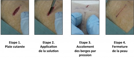
In a first experiment, the researchers compared two methods for skin closure in a deep wound: traditional sutures, and the application of the aqueous nanoparticle solution with a brush. The latter is easy to use and closes skin rapidly until it heals completely, without inflammation or necrosis. The resulting scar is almost invisible.

Phase 1 Skin injury
Phase 2 Application of the solution
Phase 3 Using pressure to hold the edges together
Phase 4 Skin closure

Schéma plaie cutanée

Illustration of the first experiment conducted by the resear chers on rats: a deep wound is repaired by applying the aqueous nanoparticle solution. The wound closes in thirty seconds.
© “Matière Molle et Chimie” Laboratory (CNRS/ESPCI Paris Tech)

In a second experiment, still on rats, the researchers applied this solution to soft-tissue organs such as the liver, lungs or spleen that are difficult to suture because they tear when the needle passes through them. At present, no glue is sufficiently strong as well as harmless for the organism. Confronted with a deep gash in the liver with severe bleeding, the researchers closed the wound by spreading the aqueous nanoparticle solution and pressing the two edges of the wound toget her. The bleeding stopped. To repair a sectioned liver lobe, the researchers also used nanoparticles: they glued a film coated with nanoparticles onto the wound, and stopped the bleeding. In both situations, organ function was unaffected and the animals survived.

“Gluing a film to stop leakage” is only one example of the possibilities opened up by adhesion brought by nanoparticles. In an entirely different field, the researchers have succeeded in using anoparticles to attach a biodegradable membrane used for cardiac cell therapy, and to achieve this despite the substantial mechanical constraints due to its beating. They thus showed that it would be possible to attach various medical devices to organs and tissues for therapeutic, repair or mechanical strengthening purposes.

This adhesion method is exceptional because of its potential spectrum of clinical applications. It is simple, easy to use and the nanoparticles employed (silica, iron oxides) can be metabolized by the organism. It can easily be integrated into ongoing research on healing and tissue regeneration and contribute to the development of regenerative medicine.

Here’s a link to and a citation for the paper,

Organ Repair, Hemostasis, and In Vivo Bonding of Medical Devices by Aqueous Solutions of Nanoparticles by Anne Meddahi-Pellé, Aurélie Legrand, Alba Marcellan, Liliane Louedec, Didier Letourneur, Ludwik Leibler. Angewandte Chemie. Published online April 16, 2014. DOI: 10.1002/anie.201401043

This article is open access.

Reducing animal testing for nanotoxicity—PETA (People for the Ethical Treatment of Animals) presentation at NanoTox 2014

Writing about nanotechnology can lead you in many different directions such as the news about PETA (People for the Ethical Treatment of Animals) and its poster presentation at the NanoTox 2014 conference being held in Antalya, Turkey from April 23 – 26, 2014. From the April 22, 2014 PETA news release on EurekAlert,

PETA International Science Consortium Ltd.’s nanotechnology expert will present a poster titled “A tiered-testing strategy for nanomaterial hazard assessment” at the 7th International Nanotoxicology Congress [NanoTox 2014] to be held April 23-26, 2014, in Antalya, Turkey.

Dr. Monita Sharma will outline a strategy consistent with the 2007 report from the US National Academy of Sciences, “Toxicity Testing in the 21st Century: A Vision and a Strategy,” which recommends use of non-animal methods involving human cells and cell lines for mechanistic pathway–based toxicity studies.

Based on the current literature, the proposed strategy includes thorough characterization of nanomaterials as manufactured, as intended for use, and as present in the final biological system; assessment using multiple in silico and in vitro model systems, including high-throughput screening (HTS) assays and 3D systems; and data sharing among researchers from government, academia, and industry through web-based tools, such as the Nanomaterial Registry and NanoHUB

Implementation of the proposed strategy will generate meaningful information on nanomaterial properties and their interaction with biological systems. It is cost-effective, reduces animal use, and can be applied for assessing risk and making intelligent regulatory decisions regarding the use and disposal of nanomaterials.

PETA’s International Science Consortium has recently launched a nanotechnology webpage which provides a good overview of the basics and, as one would expect from PETA, a discussion of relevant strategies that eliminate the use of animals in nanotoxicity assessment,

What is nano?

The concept of fabricating materials at an atomic scale was introduced in 1959 by physicist Richard Feynman in his talk entitled “There’s Plenty of Room at the Bottom.” The term “nano” originates from the Greek word for “dwarf,” which represents the very essence of nanomaterials. In the International System of Units, the prefix “nano” means one-billionth, or 10-9; therefore, one nanometer is one-billionth of a meter, which is smaller than the thickness of a sheet of paper or a strand of hair.  …

Are there different kinds of nano?

The possibility of controling biological processes using custom-synthesized materials at the nanoscale has intrigued researchers from different scientific fields. With the ever increasing sophistication of nanomaterial synthesis, there has been an exponential increase in the number and type of nanomaterials available or that can be custom synthesized. Table 1 lists some of the nanomaterials that are currently available.

….

Oddly, given the question ‘Are there different kinds of nano?’, there’s no mention of nanobots.  Still it’s understandable that they’d focus on nanomaterials which are, as far as I know, the only ‘nano’ anything tested for toxicity. On that note, PETA’s Nanotechnology page offers this revelatory listing (scroll down about 3/4 of the way),

The following are some of the web-based tools being used by nanotoxicologists and material scientists:

Getting back to the NanoTox conference being held now in Antalya, I noticed a couple of familiar names on the list of keynote speakers (scroll down about 15% of the way), Kostas Kostarelos (last mentioned in a Feb. 28, 2014 posting about scientific publishing and impact factors’ scroll down about 1/2 way) and Mark Wiesner (last mentioned in a Nov. 13, 2013 posting about a major grant for one of his projects).

Canon-Molecular Imprints deal and its impact on shrinking chips (integrated circuits)

There’s quite an interesting April 20, 2014 essay on Nanotechnology Now which provides some insight into the nanoimprinting market. I recommend reading it but for anyone who is not intimately familiar with the scene, here are a few excerpts along with my attempts to decode this insider’s (from Martini Tech) view,

About two months ago, important news shook the small but lively Japanese nanoimprint community: Canon has decided to acquire, making it a wholly-owned subsidiary, Texas-based Molecular Imprints, a strong player in the nanotechnology industry and one of the main makers of nanoimprint devices such as the Imprio 450 and other models.

So, Canon, a Japanese company, has made a move into the nanoimpriting sector by purchasing Molecular Imprints, a US company based in Texas, outright.

This next part concerns the expiration of Moore’s Law (i.e., every 18 months computer chips get smaller and faster) and is why the major chip makers are searching for new solutions as per the fifth paragraph in this excerpt,

Molecular Imprints` devices are aimed at the IC [integrated circuits, aka chips, I think] patterning market and not just at the relatively smaller applications market to which nanoimprint is usually confined: patterning of bio culture substrates, thin film applications for the solar industry, anti-reflection films for smartphone and LED TV screens, patterning of surfaces for microfluidics among others.

While each one of the markets listed above has the potential of explosive growth in the medium-long term future, at the moment none of them is worth more than a few percentage points, at best, of the IC patterning market.

The mainstream technology behind IC patterning is still optical stepper lithography and the situation is not likely to change in the near term future.

However, optical lithography has its limitations, the main challenge to its 40-year dominance not coming only from technological and engineering issues, but mostly from economical ones.

While from a strictly technological point of view it may still be possible for the major players in the chip industry (Intel, GF, TSMC, Nvidia among others) to go ahead with optical steppers and reach the 5nm node using multi-patterning and immersion, the cost increases associated with each die shrink are becoming staggeringly high.

A top-of-the-notch stepper in the early 90s could have been bought for a few millions of dollars, now the price has increased to some tens of millions for the top machines

The essay describes the market impact this acquisition may have for Canon,

Molecular Imprints has been a company on the forefront of commercialization of nanoimprint-based solutions for IC manufacturing, but so far their solutions have yet to become a viable alternative HVM IC manufacturing market.

The main stumbling blocks for IC patterning using nanoimprint technology are: the occurrence of defects on the mask that inevitably replicates them on each substrate and the lack of alignment precision between the mold and the substrate needed to pattern multi-layered structures.

Therefore, applications for nanoimprint have been limited to markets where no non-periodical structure patterning is needed and where one-layered patterning is sufficient.

But the big market where everyone is aiming for is, of course, IC patterning and this is where much of the R&D effort goes.

While logic patterning with nanoimprint may still be years away, simple patterning of NAND structures may be feasible in the near future, and the purchase of Molecular Imprints by Canon is a step in this direction

Patterning of NAND structures may still require multi-layered structures, but the alignment precision needed is considerably lower than logic.

Moreover, NAND requirements for defectivity are more relaxed than for logic due to the inherent redundancy of the design, therefore, NAND manufacturing is the natural first step for nanoimprint in the IC manufacturing market and, if successful, it may open a whole new range of opportunities for the whole sector.

Assuming I’ve read the rest of this essay rightly, here’s my summary: there are a number of techniques being employed to make chips smaller and more efficient. Canon has purchased a company that is versed in a technique that creates NAND (you can find definitions here) structures in the hope that this technique can be commercialized so that Canon becomes dominant in the sector because (1) they got there first and/or because (2) NAND manufacturing becomes a clear leader, crushing competition from other technologies. This could cover short-term goals and, I imagine Canon hopes, long-term goals.

It was a real treat coming across this essay as it’s an insider’s view. So, thank you to the folks at Martini Tech who wrote this. You can find Molecular Imprints here.

Geckskin update

It appears that researchers at the University of Massachusetts at Amherst have found a way to make their ‘Geckskin’, an adhesive product modeled on a gecko’s feet (a lizard famously able to stick to an object by a single toe), adhere to the widest range of surfaces yet (from an April 17, 2014 University of Massachusetts news release [also on EurekAlert but dated April 18, 2014]),

The ability to stick objects to a wide range of surfaces such as drywall, wood, metal and glass with a single adhesive has been the elusive goal of many research teams across the world, but now a team of University of Massachusetts Amherst inventors describe a new, more versatile version of their invention, Geckskin, that can adhere strongly to a wider range of surfaces, yet releases easily, like a gecko’s feet.

“Imagine sticking your tablet on a wall to watch your favorite movie and then moving it to a new location when you want, without the need for pesky holes in your painted wall,” says polymer science and engineering professor Al Crosby. Geckskin is a ‘gecko-like,’ reusable adhesive device that they had previously demonstrated can hold heavy loads on smooth surfaces such as glass.

‘Geckskin’ first mentioned here in an April 3, 2012 posting features a different approach to mimicking the gecko’s adhesiveness; most teams are focused on the nanoscopic hairs on the gecko’s feet while the researchers at the University of Massachusetts have worked on ‘draping’,

The University of Massachusetts team’s innovation (from the Feb. 17, 2012 news item),

The key innovation by Bartlett and colleagues was to create an integrated adhesive with a soft pad woven into a stiff fabric, which allows the pad to “drape” over a surface to maximize contact. Further, as in natural gecko feet, the skin is woven into a synthetic “tendon,” yielding a design that plays a key role in maintaining stiffness and rotational freedom, the researchers explain.

Importantly, the Geckskin’s adhesive pad uses simple everyday materials such as polydimethylsiloxane (PDMS), which holds promise for developing an inexpensive, strong and durable dry adhesive.

The UMass Amherst researchers are continuing to improve their Geckskin design by drawing on lessons from the evolution of gecko feet, which show remarkable variation in anatomy. “Our design for Geckskin shows the true integrative power of evolution for inspiring synthetic design that can ultimately aid humans in many ways,” says Irschick.

Two years later, the researchers have proved their concept across a range of surfaces (from the 2014 news release),

In Geckskin, the researchers created this ability by combining soft elastomers and ultra-stiff fabrics such as glass or carbon fiber fabrics. By “tuning” the relative stiffness of these materials, they can optimize Geckskin for a range of applications, the inventors say.

To substantiate their claims of Geckskin’s properties, the UMass Amherst team compared three versions to the abilities of a living Tokay gecko on several surfaces, as described in their journal article this month. As predicted by their theory, one Geckskin version matches and even exceeds the gecko’s performance on all tested surfaces.

Irschick points out, “The gecko’s ability to stick to a variety of surfaces is critical for its survival, but it’s equally important to be able to release and re-stick whenever it wants. Geckskin displays the same ability on different commonly used surfaces, opening up great possibilities for new technologies in the home, office or outdoors.”

Here’s a link to and a citation for the paper,

Creating Gecko-Like Adhesives for “Real World” Surfaces by Daniel R. King, Michael D. Bartlett, Casey A. Gilman, Duncan J. Irschick, and Alfred J. Crosby. Advanced Materials. Article first published online: 17 APR 2014 DOI: 10.1002/adma.201306259

© 2014 WILEY-VCH Verlag GmbH & Co. KGaA, Weinheim

This article is behind a paywall.

The researchers have produced a video (silent) where they demonstrate the Geckskin’s adhesive properties over a number of different surfaces. At seven minutes or so, it runs a bit longer than the videos I embed here but you can find it at http://www.youtube.com/watch?v=SayqhqTZoxI&feature=youtu.be.

The Irish mix up some graphene

There was a lot of excitement (one might almost call it giddiness) earlier this week about a new technique from Irish researchers for producing graphene. From an April 20, 2014 article by Jacob Aron for New Scientist (Note: A link has been removed),

First, pour some graphite powder into a blender. Add water and dishwashing liquid, and mix at high speed. Congratulations, you just made the wonder material graphene.

This surprisingly simple recipe is now the easiest way to mass-produce pure graphene – sheets of carbon just one atom thick. The material has been predicted to revolutionise the electronics industry, based on its unusual electrical and thermal properties. But until now, manufacturing high-quality graphene in large quantities has proved difficult – the best lab techniques manage less than half a gram per hour.

“There are companies producing graphene at much higher rates, but the quality is not exceptional,” says Jonathan Coleman of Trinity College Dublin in Ireland.

Coleman’s team was contracted by Thomas Swan, a chemicals firm based in Consett, UK, to come up with something better. From previous work they knew that it is possible to shear graphene from graphite, the form of carbon found in pencil lead. Graphite is essentially made from sheets of graphene stacked together like a deck of cards, and sliding it in the right way can separate the layers.

Rachel Courtland chimes in with her April 21,2014 post for the Nanoclast blog (on the IEEE [Institute of Electrical and Electronics Engineers]) website (Note: A link has been removed),

The first graphene was made by pulling layers off of graphite using Scotch tape. Now, in keeping with the low-tech origins of the material, a team at Trinity College Dublin has found that it should be possible to make large quantities of the stuff by mixing up some graphite and stabilizing detergent with a blender.

The graphene produced in this manner isn’t anything like the wafer-scale sheets of single-layer graphene that are being grown by Samsung, IBM and others for high-performance electronics. Instead, the blender-made variety consists of small flakes that are exfoliated off of bits of graphite and then separated out by centrifuge. But small-scale graphene has its place, the researchers say. …

An April 22, 2014 CRANN (the Centre for Research on Adaptive Nanostructures and Nanodevices) at Trinity College Dublin news release (also on Nanowerk as an April 20, 2014 news item) provides more details about the new technique and about the private/public partnership behind it,

Research team led by Prof Jonathan Coleman discovers new research method to produce large volumes of high quality graphene.

Researchers in AMBER, the Science Foundation Ireland funded materials science centre headquartered at CRANN, Trinity College Dublin have, for the first time, developed a new method of producing industrial quantities of high quality graphene. …

The discovery will change the way many consumer and industrial products are manufactured. The materials will have a multitude of potential applications including advanced food packaging; high strength plastics; foldable touch screens for mobile phones and laptops; super-protective coatings for wind turbines and ships; faster broadband and batteries with dramatically higher capacity than anything available today.

Thomas Swan Ltd. has worked with the AMBER research team for two years and has signed a license agreement to scale up production and make the high quality graphene available to industry globally. The company has already announced two new products as a result of the research discovery (Elicarb®Graphene Powder and Elicarb® Graphene Dispersion).

Until now, researchers have been unable to produce graphene of high quality in large enough quantities. The subject of on-going international research, the research undertaken by AMBER is the first to perfect a large-scale production of pristine graphene materials and has been highlighted by the highly prestigious Nature Materials publication as a global breakthrough. Professor Coleman and his team used a simple method for transforming flakes of graphite into defect-free graphene using commercially available tools, such as high-shear mixers. They demonstrated that not only could graphene-containing liquids be produced in standard lab-scale quantities of a few 100 millilitres, but the process could be scaled up to produce 100s of litres and beyond.

Minister for Research and Innovation Sean Sherlock, TD commented; “Professor Coleman’s discovery shows that Ireland has won the worldwide race on the production of this ‘miracle material’. This is something that USA, China, Australia, UK, Germany and other leading nations have all been striving for and have not yet achieved. This announcement shows how the Irish Government’s strategy of focusing investment in science with impact, as well as encouraging industry and academic collaboration, is working.”

Here’s a link to and a citation for the researchers’ paper,

Scalable production of large quantities of defect-free few-layer graphene by shear exfoliation in liquids by Keith R. Paton, Eswaraiah Varrla, Claudia Backes, Ronan J. Smith, Umar Khan, Arlene O’Neill, Conor Boland, Mustafa Lotya, Oana M. Istrate, Paul King, Tom Higgins, Sebastian Barwich, Peter May, Pawel Puczkarski, Iftikhar Ahmed, Matthias Moebius, Henrik Pettersson, Edmund Long, João Coelho, Sean E. O’Brien, Eva K. McGuire, Beatriz Mendoza Sanchez, Georg S. Duesberg, Niall McEvoy, Timothy J. Pennycook, et al. Nature Materials (2014) doi:10.1038/nmat3944 Published online 20 April 2014

This article is mostly behind a paywall but there is a free preview available through ReadCube Access.

For anyone who’s curious about AMBER, here’s more from the About Us page on the CRANN website (Note: A link has been removed),

In October 2013, a new Science Foundation Ireland funded research centre, AMBER (Advanced Materials and BioEngineering Research) was launched. AMBER is jointly hosted in TCD [Trinity College Dublin] by CRANN and the Trinity Centre for Bioenineering, and works in collaboration with the Royal College of Surgeons in Ireland and UCC. The centre provides a partnership between leading researchers in materials science and industry and will deliver internationally leading research that will be industrially and clinically informed with outputs including new discoveries and devices in ICT, medical device and industrial technology sectors.

Finally, Thomas Swan Ltd. can be found here.
Wilson Center hosts ‘Environmental Information: The Roles of Experts and the Public’ on April 29, 2014

Here’s a description of the Wilson Center event, Environmental Information: The Roles of Experts and the Public,

Access to environmental information and use of it for environmental decision making are central pillars of environmental democracy. Yet, not much attention is paid to the question of who is producing it, and for whom? By examining the history of environmental information, since NEPA in 1969, three eras can be identified: information produced by experts, for experts (1969-1992); information produced by experts, to be shared by experts and the public (1992-2011); and finally, information produced by experts and the public to be shared by experts and the public.

Underlying these are changes in access to information, rise in levels of education and rapid change due to digital technologies. The three eras and their implication to environmental decision making will be explored, with special attention to the role of geographical information and geographical information systems and to citizen science.  [emphasis mine]

Tuesday, April 29th from 10:00 – 11:30am. [EST]

I hope the speaker description and the paper being distributed on the event page mean this may be a bit more interesting to those of us curious about citizen science than is immediately apparent from the event description,

Muki (Mordechai) Haklay

Muki Haklay is a Professor of Geographic Information Science in the Department of Civil, Environmental and Geomatic Engineering, University College London.  He is also the Director of the UCL Extreme Citizen Science group, which is dedicated to allowing any community, regardless of their literacy, to use scientific methods and tools to collect, analyze and interpret and use information about their area and activities.

His research interests include Public access and use of Environmental Information; Human-Computer Interaction (HCI) and Usability Engineering aspects of GIS; and Societal aspects of GIS use – in particular, participatory mapping and Citizen Science.

Here’s the paper,

Citizen Science and Volunteered Geographic Information – overview and typology of participation

You can RSVP from the event page if you’re planning to attend this event in Washington, DC in person, alternatively you can watch a livestream webcast by returning to the event page on April 29, 2014 at 10 am (that will be 7 am, if you’re on the West Coast),

Move over laser—the graphene/carbon nanotube spaser is here, on your t-shirt

This research graphene/carbon nanotube research comes from Australia according to an April 16, 2014 news item on Nanowerk,

A team of researchers from Monash University’s [Australia] Department of Electrical and Computer Systems Engineering (ECSE) has modelled the world’s first spaser …

An April 16, 2014 Monash University news release, which originated the new item, describes the spaser and its relationship to lasers,,

A new version of “spaser” technology being investigated could mean that mobile phones become so small, efficient, and flexible they could be printed on clothing.

A spaser is effectively a nanoscale laser or nanolaser. It emits a beam of light through the vibration of free electrons, rather than the space-consuming electromagnetic wave emission process of a traditional laser.

The news release also provides more details about the graphene/carbon nanotube spaser research and the possibility of turning t-shirts into telephones,

PhD student and lead researcher Chanaka Rupasinghe said the modelled spaser design using carbon would offer many advantages.

“Other spasers designed to date are made of gold or silver nanoparticles and semiconductor quantum dots while our device would be comprised of a graphene resonator and a carbon nanotube gain element,” Chanaka said.

“The use of carbon means our spaser would be more robust and flexible, would operate at high temperatures, and be eco-friendly.

“Because of these properties, there is the possibility that in the future an extremely thin mobile phone could be printed on clothing.”

Spaser-based devices can be used as an alternative to current transistor-based devices such as microprocessors, memory, and displays to overcome current miniaturising and bandwidth limitations.

The researchers chose to develop the spaser using graphene and carbon nanotubes. They are more than a hundred times stronger than steel and can conduct heat and electricity much better than copper. They can also withstand high temperatures.

Their research showed for the first time that graphene and carbon nanotubes can interact and transfer energy to each other through light. These optical interactions are very fast and energy-efficient, and so are suitable for applications such as computer chips.

“Graphene and carbon nanotubes can be used in applications where you need strong, lightweight, conducting, and thermally stable materials due to their outstanding mechanical, electrical and optical properties. They have been tested as nanoscale antennas, electric conductors and waveguides,” Chanaka said.

Chanaka said a spaser generated high-intensity electric fields concentrated into a nanoscale space. These are much stronger than those generated by illuminating metal nanoparticles by a laser in applications such as cancer therapy.

“Scientists have already found ways to guide nanoparticles close to cancer cells. We can move graphene and carbon nanotubes following those techniques and use the high concentrate fields generated through the spasing phenomena to destroy individual cancer cells without harming the healthy cells in the body,” Chanaka said

Here’s a link to and a citation for the paper,

Spaser Made of Graphene and Carbon Nanotubes by Chanaka Rupasinghe, Ivan D. Rukhlenko, and Malin Premaratne. ACS Nano, 2014, 8 (3), pp 2431–2438. DOI: 10.1021/nn406015d Publication Date (Web): February 23, 2014
Copyright © 2014 American Chemical Society

This paper is behind a paywall.

Chiral breathing at the Institute of Physical Chemistry of the Polish Academy of Sciences (IPC PAS)

An April 17, 2014 news item on ScienceDaily highlights some research about a polymer that has some special properties,

Electrically controlled glasses with continuously adjustable transparency, new polarisation filters, and even chemosensors capable of detecting single molecules of specific chemicals could be fabricated thanks to a new polymer unprecedentedly combining optical and electrical properties.

An international team of chemists from Italy, Germany, and Poland developed a polymer with unique optical and electric properties. Components of this polymer change their spatial configuration depending on the electric potential applied. In turn, the polarisation of transmitted light is affected. The material can be used, for instance, in polarisation filters and window glasses with continuously adjustable transparency. Due to its mechanical properties, the polymer is also perfectly suitable for fabrication of chemical sensors for selective detection and determination of optically active (chiral) forms of an analyte.

The research findings of the international team headed by Prof. Francesco Sannicolo from the Universita degli Studi di Milano were recently published in Angewandte Chemie International Edition.

“Until now, to give polymers chiral properties, chiral pendants were attached to the polymer backbone. In such designs the polymer was used as a scaffold only. Our polymer is exceptional, with chirality inherent to it, and with no pending groups. The polymer is both a scaffold and an optically active chiral structure. Moreover, the polymer conducts electricity,” comments Prof. Włodzimierz Kutner from the Institute of Physical Chemistry of the Polish Academy of Sciences (IPC PAS) in Warsaw, one of the initiators of the research.

An April 17, 2014 IPC PAS news release (also on EurrekAlert), which originated the news item, describes chirality and the breathing metaphor with regard to this new polymer,

Chirality can be best explained by referring to mirror reflection. If two varieties of the same object look like their mutual mirror images, they differ in chirality. Human hands provide perhaps the most universal example of chirality, and the difference between the left and right hand becomes obvious if we try to place a left-handed glove on a right hand. The same difference as between the left and right hand is between two chiral molecules with identical chemical composition. Each of them shows different optical properties, and differently rotates plane-polarised light. In such a case, chemists refer to one chemical compound existing as two optical isomers called enantiomers.

The polymer presented by Prof. Sannicolo’s team was developed on the basis of thiophene, an organic compound composed of a five-member aromatic ring containing a sulphur atom. Thiophene polymerisation gives rise to a chemically stable polymer of high conductivity. The basic component of the new polymer – its monomer – is made of a dimer with two halves each made of two thiophene rings and one thianaphthene unit. The halves are connected at a single point and can partially be rotated with respect to each other by applying electric potential. Depending on the orientation of the halves, the new polymer either assumes or looses chirality. This behaviour is fully reversible and resembles a breathing system, whereas the “chiral breathing” is controlled by an external electric potential.

The development of a new polymer was initiated thanks to the research on molecular imprinting pursued at the Institute of Physical Chemistry of the PAS. The research resulted, for instance, in the development of polymers used as recognising units (receptors) in chemosensors, capable of selective capturing of molecules of various analytes, for instance nicotine, and also melamine, an ill-reputed chemical detrimental to human health, used as an additive to falsify protein content in milk and dairy products produced in China.

Generally, molecular imprinting consists in creating template-shaped cavities in polymer matrices with molecules of interest used first as cavity templates. Subsequently these templates are washed out from the polymer. As a result, the polymer contains traps with a shape and size matching those of molecules of the removed template. To be used as a receptor in chemosensor to recognize analyte molecules similar to templates or templates themselves, the polymer imprinted with these cavities must show a sufficient mechanical strength.

“Three-dimensional networks we attempted to build at the IPC PAS using existing two-dimensional thiophene derivatives just collapsed after the template molecules were removed. That’s why we asked for assistance our Italian partners, specialising in the synthesis of thiophene derivatives. The problem was to design and synthesise a three-dimensional thiophene derivative that would allow us for cross-linking of our polymers in three dimensions. The thiophene derivative synthesised in Milan has a stable three-dimensional structure, and the controllable chiral properties of the new polymer obtained after the derivative was polymerised, turned out a nice surprise for all of us”, explains Prof. Kutner.

Here’s a link to and a citation for the paper,

Potential-Driven Chirality Manifestations and Impressive Enantioselectivity by Inherently Chiral Electroactive Organic Films by  Prof. Francesco Sannicolò1, Serena Arnaboldi, Prof. Tiziana Benincori, Dr. Valentina Bonometti, Dr. Roberto Cirilli, Prof. Lothar Dunsch, Prof. Włodzimierz Kutner, Prof. Giovanna Longhi, Prof. Patrizia R. Mussini, Dr. Monica Panigati, Prof. Marco Pierini, and Dr. Simona Rizzo. Angewandte Chemie International Edition Volume 53, Issue 10, pages 2623–2627, March 3, 2014. Article first published online: 5 FEB 2014 DOI: 10.1002/anie.201309585

© 2014 WILEY-VCH Verlag GmbH & Co. KGaA, Weinheim

This article is behind a paywall.