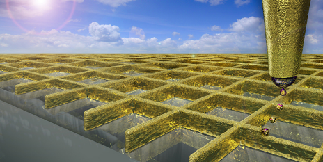
An announcement about European Union funding for a project to reproduce neural networks by 3D nanoprinting can be found in a June 10, 2016 news item on Nanowerk,
The MESO-BRAIN consortium has received a prestigious award of €3.3million in funding from the European Commission as part of its Future and Emerging Technology (FET) scheme. The project aims to develop three-dimensional (3D) human neural networks with specific biological architecture, and the inherent ability to interrogate the network’s brain-like activity both electrophysiologically and optically. It is expected that the MESO-BRAIN will facilitate a better understanding of human disease progression, neuronal growth and enable the development of large-scale human cell-based assays to test the modulatory effects of pharmacological and toxicological compounds on neural network activity. The use of more physiologically relevant human models will increase drug screening efficiency and reduce the need for animal testing.
A June 9, 2016 Institute of Photonic Sciences (ICFO) press release (also on EurekAlert), which originated the news item, provides more detail,
About the MESO-BRAIN project
The MESO-BRAIN project’s cornerstone will use human induced pluripotent stem cells (iPSCs) that have been differentiated into neurons upon a defined and reproducible 3D scaffold to support the development of human neural networks that emulate brain activity. The structure will be based on a brain cortical module and will be unique in that it will be designed and produced using nanoscale 3D-laser-printed structures incorporating nano-electrodes to enable downstream electrophysiological analysis of neural network function. Optical analysis will be conducted using cutting-edge light sheet-based, fast volumetric imaging technology to enable cellular resolution throughout the 3D network. The MESO-BRAIN project will allow for a comprehensive and detailed investigation of neural network development in health and disease.
Prof Edik Rafailov, Head of the MESO-BRAIN project (Aston University) said: “What we’re proposing to achieve with this project has, until recently, been the stuff of science fiction. Being able to extract and replicate neural networks from the brain through 3D nanoprinting promises to change this. The MESO-BRAIN project has the potential to revolutionise the way we are able to understand the onset and development of disease and discover treatments for those with dementia or brain injuries. We cannot wait to get started!”
The MESO-BRAIN project will launch in September 2016 and research will be conducted over three years.
About the MESO-BRAIN consortium
Each of the consortium partners have been chosen for the highly specific skills & knowledge that they bring to this project. These include technologies and expertise in stem cells, photonics, physics, 3D nanoprinting, electrophysiology, molecular biology, imaging and commercialisation.
Aston University (UK) Aston Institute of Photonic Technologies (School of Engineering and Applied Science) is one of the largest photonic groups in UK and an internationally recognised research centre in the fields of lasers, fibre-optics, high-speed optical communications, nonlinear and biomedical photonics. The Cell & Tissue Biomedical Research Group (Aston Research Centre for Healthy Ageing) combines collective expertise in genetic manipulation, tissue engineering and neuronal modelling with the electrophysiological and optical analysis of human iPSC-derived neural networks. Axol Bioscience Ltd. (UK) was founded to fulfil the unmet demand for high quality, clinically relevant human iPSC-derived cells for use in biomedical research and drug discovery. The Laser Zentrum Hannover (Germany) is a leading research organisation in the fields of laser development, material processing, laser medicine, and laser-based nanotechnologies. The Neurophysics Group (Physics Department) at University of Barcelona (Spain) are experts in combing experiments with theoretical and computational modelling to infer functional connectivity in neuronal circuits. The Institute of Photonic Sciences (ICFO) (Spain) is a world-leading research centre in photonics with expertise in several microscopy techniques including light sheet imaging. KITE Innovation (UK) helps to bridge the gap between the academic and business sectors in supporting collaboration, enterprise, and knowledge-based business development.
For anyone curious about the FET funding scheme, there’s this from the press release,
Horizon 2020 aims to ensure Europe produces world-class science by removing barriers to innovation through funding programmes such as the FET. The FET (Open) funds forward-looking collaborations between advanced multidisciplinary science and cutting-edge engineering for radically new future technologies. The published success rate is below 1.4%, making it amongst the toughest in the Horizon 2020 suite of funding schemes. The MESO-BRAIN proposal scored a perfect 5/5.
You can find out more about the MESO-BRAIN project on its ICFO webpage.
They don’t say anything about it but I can’t help wondering if the scientists aren’t also considering the possibility of creating an artificial brain.

![[downloaded from https://github.com/jhermann/Stack-O-Waffles] Credit: jherman](http://www.frogheart.ca/wp-content/uploads/2016/01/Waffles.png)