Tag Archives: Alex Zettl

A nano big bang event

Here’s what you’re seeing (from the YouTube entry),

Berkeley Lab scientists and collaborators took advantage of one of the best microscopes in the world – the TEAM I electron microscope at the Molecular Foundry – to watch how individual gold atoms organized themselves into crystals on top of graphene. The research team observed as groups of gold atoms formed and broke apart many times, trying out different configurations, before finally stabilizing. The discovery of this fast-changing and reversible process was possible thanks to these high-speed images captured at atomic resolution. Credit: Berkeley Lab

The work was announced in a March 25, 2021 news item on phys.org,

When we grow crystals, atoms first group together into small clusters—a process called nucleation. But understanding exactly how such atomic ordering emerges from the chaos of randomly moving atoms has long eluded scientists.

Classical nucleation theory suggests that crystals form one atom at a time, steadily increasing the level of order. Modern studies have also observed a two-step nucleation process, where a temporary, high-energy structure forms first, which then changes into a stable crystal. But according to an international research team co-led by the Department of Energy’s Lawrence Berkeley National Laboratory (Berkeley Lab), the real story is even more complicated.

Their findings, recently reported in the journal Science, reveal that rather than grouping together one-by-one or making a single irreversible transition, gold atoms will instead self-organize, fall apart, regroup, and then reorganize many times before establishing a stable, ordered crystal. Using an advanced electron microscope, the researchers witnessed this rapid, reversible nucleation process for the first time. Their work provides tangible insights into the early stages of many growth processes such as thin-film deposition and nanoparticle formation.

A March 25, 2021 DOE [US Dept. of Energy]/Lawrence Berkeley National Laboratory news release (also on EurekAlert) by Clarissa Bhargava, which originated the news item, expands on the topic,

“As scientists seek to control matter at smaller length scales to produce new materials and devices, this study helps us understand exactly how some crystals form,” said Peter Ercius, one of the study’s lead authors and a staff scientist at Berkeley Lab’s Molecular Foundry.

In line with scientists’ conventional understanding, once the crystals in the study reached a certain size, they no longer returned to the disordered, unstable state. Won Chul Lee, one of the professors guiding the project, describes it this way: if we imagine each atom as a Lego brick, then instead of building a house one brick at a time, it turns out that the bricks repeatedly fit together and break apart again until they are finally strong enough to stay together. Once the foundation is set, however, more bricks can be added without disrupting the overall structure.

The unstable structures were only visible because of the speed of newly developed detectors on the TEAM I [Transmission Electron Aberration-corrected Microscope], one of the world’s most powerful electron microscopes. A team of in-house experts guided the experiments at the National Center for Electron Microscopy in Berkeley Lab’s Molecular Foundry. Using the TEAM I microscope, researchers captured real-time, atomic-resolution images at speeds up to 625 frames per second, which is exceptionally fast for electron microcopy and about 100 times faster than previous studies. The researchers observed individual gold atoms as they formed into crystals, broke apart into individual atoms, and then reformed again and again into different crystal configurations before finally stabilizing.

“Slower observations would miss this very fast, reversible process and just see a blur instead of the transitions, which explains why this nucleation behavior has never been seen before,” said Ercius.

The reason behind this reversible phenomenon is that crystal formation is an exothermic process – that is, it releases energy. In fact, the very energy released when atoms attach to the tiny nuclei can raise the local “temperature” and melt the crystal. In this way, the initial crystal formation process works against itself, fluctuating between order and disorder many times before building a nucleus that is stable enough to withstand the heat. The research team validated this interpretation of their experimental observations by performing calculations of binding reactions between a hypothetical gold atom and a nanocrystal.

Now, scientists are developing even faster detectors which could be used to image the process at higher speeds. This could help them understand if there are more features of nucleation hidden in the atomic chaos. The team is also hoping to spot similar transitions in different atomic systems to determine whether this discovery reflects a general process of nucleation.

One of the study’s lead authors, Jungwon Park, summarized the work: “From a scientific point of view, we discovered a new principle of crystal nucleation process, and we proved it experimentally.”

Here’s a link to and a citation for the paper,

Reversible disorder-order transitions in atomic crystal nucleation by Sungho Jeon, Taeyeong Heo, Sang-Yeon Hwang, Jim Ciston, Karen C. Bustillo, Bryan W. Reed, Jimin Ham, Sungsu Kang, Sungin Kim, Joowon Lim, Kitaek Lim, Ji Soo Kim, Min-Ho Kang, Ruth S. Bloom, Sukjoon Hong, Kwanpyo Kim, Alex Zettl, Woo Youn Kim, Peter Ercius, Jungwon Park, Won Chul Lee. Science 29 Jan 2021: Vol. 371, Issue 6528, pp. 498-503 DOI: 10.1126/science.aaz7555

This paper is behind a paywall.
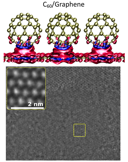
Psst: secret marriage … Buckyballs and Graphene get together!

A March 1, 2018 news item on Nanowerk announces  a new coupling,

Scientists combined buckyballs, [also known as buckminsterfullerenes, fullerenes, or C60] which resemble tiny soccer balls made from 60 carbon atoms, with graphene, a single layer of carbon, on an underlying surface. Positive and negative charges can transfer between the balls and graphene depending on the nature of the surface as well as the structural order and local orientation of the carbon ball. Scientists can use this architecture to develop tunable junctions for lightweight electronic devices.

The researchers have made this illustration of their work available,

Researchers are developing new, lightweight electronics that rapidly conduct electricity by covering a sheet of carbon (graphene) with buckyballs. Electricity is the flow of electrons. On these lightweight structures, electrons as well as positive holes (missing electrons) transfer between the balls and graphene. The team showed that the crystallinity and orientation of the balls, as well as the underlying layer, affected this charge transfer. The top image shows a calculation of the charge density for a specific orientation of the balls on graphene. The blue represents positive charges, while the red is negative. The bottom image shows that the balls are in a close-packed structure. The bright dots correspond to the projected images of columns of buckyball molecules. Courtesy: US Department of Energy Office of Science

A February 28, 2018 US Department of Energy (DoE) Office of Science news release, which originated the news item, provides more detail,

The Impact

Fast-moving electrons and their counterpart, holes, were preserved in graphene with crystalline buckyball overlayers. Significantly, the carbon ball provides charge transfer to the graphene. Scientists expect the transfer to be highly tunable with external voltages. This marriage has ramifications for smart electronics that run longer and do not break as easily, bringing us closer to sensor-embedded smart clothing and robotic skin.

Summary

Charge transfer at the interface between dissimilar materials is at the heart of almost all electronic technologies such as transistors and photovoltaic devices. In this study, scientists studied charge transfer at the interface region of buckyball molecules deposited on graphene, with and without a supporting substrate, such as hexagonal boron nitride. They employed ab initio density functional theory with van der Waals interactions to model the structure theoretically. Van der Waals interactions are weak connections between neutral molecules. The team used high-resolution transmission electron microscopy and electronic transport measurements to characterize experimentally the properties of the interface. The researchers observed that charge transfer between buckyballs and the graphene was sensitive to the nature of the underlying substrate, in addition, to the crystallinity and local orientation of the buckyballs. These studies open an avenue to devices where buckyball layers on top of graphene can serve as electron acceptors and other buckyball layers as electron donors. Even at room temperature, buckyball molecules were orientationally locked into position. This is in sharp contrast to buckyball molecules in un-doped bulk crystalline configurations, where locking occurs only at low temperature. High electron and hole mobilities are preserved in graphene with crystalline buckyball overlayers. This finding has ramifications for the development of organic high-mobility field-effect devices and other high mobility applications.

Here’s a link to and a citation for the paper,

Molecular Arrangement and Charge Transfer in C60 /Graphene Heterostructures by Claudia Ojeda-Aristizabal, Elton J. G. Santos, Seita Onishi, Aiming Yan, Haider I. Rasool, Salman Kahn, Yinchuan Lv, Drew W. Latzke, Jairo Velasco Jr., Michael F. Crommie, Matthew Sorensen, Kenneth Gotlieb, Chiu-Yun Lin, Kenji Watanabe, Takashi Taniguchi, Alessandra Lanzara, and Alex Zettl. ACS Nano, 2017, 11 (5), pp 4686–4693 DOI: 10.1021/acsnano.7b00551 Publication Date (Web): April 24, 2017

Copyright © 2017 American Chemical Society

This paper is behind a paywall.

SINGLE (3D Structure Identification of Nanoparticles by Graphene Liquid Cell Electron Microscopy) and the 3D structures of two individual platinum nanoparticles in solution

It seems to me there’s been an explosion of new imaging techniques lately. This one from the Lawrence Berkelely National Laboratory is all about imaging colloidal nanoparticles (nanoparticles in solution), from a July 20, 2015 news item on Azonano,

Just as proteins are one of the basic building blocks of biology, nanoparticles can serve as the basic building blocks for next generation materials. In keeping with this parallel between biology and nanotechnology, a proven technique for determining the three dimensional structures of individual proteins has been adapted to determine the 3D structures of individual nanoparticles in solution.

A multi-institutional team of researchers led by the U.S. Department of Energy (DOE)’s Lawrence Berkeley National Laboratory (Berkeley Lab), has developed a new technique called “SINGLE” that provides the first atomic-scale images of colloidal nanoparticles. SINGLE, which stands for 3D Structure Identification of Nanoparticles by Graphene Liquid Cell Electron Microscopy, has been used to separately reconstruct the 3D structures of two individual platinum nanoparticles in solution.

A July 16, 2015 Berkeley Lab news release, which originated the news item, reveals more details about the reason for the research and the research itself,

“Understanding structural details of colloidal nanoparticles is required to bridge our knowledge about their synthesis, growth mechanisms, and physical properties to facilitate their application to renewable energy, catalysis and a great many other fields,” says Berkeley Lab director and renowned nanoscience authority Paul Alivisatos, who led this research. “Whereas most structural studies of colloidal nanoparticles are performed in a vacuum after crystal growth is complete, our SINGLE method allows us to determine their 3D structure in a solution, an important step to improving the design of nanoparticles for catalysis and energy research applications.”

Alivisatos, who also holds the Samsung Distinguished Chair in Nanoscience and Nanotechnology at the University of California Berkeley, and directs the Kavli Energy NanoScience Institute at Berkeley (Kavli ENSI), is the corresponding author of a paper detailing this research in the journal Science. The paper is titled “3D Structure of Individual Nanocrystals in Solution by Electron Microscopy.” The lead co-authors are Jungwon Park of Harvard University, Hans Elmlund of Australia’s Monash University, and Peter Ercius of Berkeley Lab. Other co-authors are Jong Min Yuk, David Limmer, Qian Chen, Kwanpyo Kim, Sang Hoon Han, David Weitz and Alex Zettl.

Colloidal nanoparticles are clusters of hundreds to thousands of atoms suspended in a solution whose collective chemical and physical properties are determined by the size and shape of the individual nanoparticles. Imaging techniques that are routinely used to analyze the 3D structure of individual crystals in a material can’t be applied to suspended nanomaterials because individual particles in a solution are not static. The functionality of proteins are also determined by their size and shape, and scientists who wanted to image 3D protein structures faced a similar problem. The protein imaging problem was solved by a technique called “single-particle cryo-electron microscopy,” in which tens of thousands of 2D transmission electron microscope (TEM) images of identical copies of an individual protein or protein complex frozen in random orientations are recorded then computationally combined into high-resolution 3D reconstructions. Alivisatos and his colleagues utilized this concept to create their SINGLE technique.

“In materials science, we cannot assume the nanoparticles in a solution are all identical so we needed to develop a hybrid approach for reconstructing the 3D structures of individual nanoparticles,” says co-lead author of the Science paper Peter Ercius, a staff scientist with the National Center for Electron Microscopy (NCEM) at the Molecular Foundry, a DOE Office of Science User Facility.

“SINGLE represents a combination of three technological advancements from TEM imaging in biological and materials science,” Ercius says. “These three advancements are the development of a graphene liquid cell that allows TEM imaging of nanoparticles rotating freely in solution, direct electron detectors that can produce movies with millisecond frame-to-frame time resolution of the rotating nanocrystals, and a theory for ab initio single particle 3D reconstruction.”

The graphene liquid cell (GLC) that helped make this study possible was also developed at Berkeley Lab under the leadership of Alivisatos and co-author Zettl, a physicist who also holds joint appointments with Berkeley Lab, UC Berkeley and Kavli ENSI. TEM imaging uses a beam of electrons rather than light for illumination and magnification but can only be used in a high vacuum because molecules in the air disrupt the electron beam. Since liquids evaporate in high vacuum, samples in solutions must be hermetically sealed in special solid containers – called cells – with a very thin viewing window before being imaged with TEM. In the past, liquid cells featured silicon-based viewing windows whose thickness limited resolution and perturbed the natural state of the sample materials. The GLC developed at Berkeley lab features a viewing window made from a graphene sheet that is only a single atom thick.

“The GLC provides us with an ultra-thin covering of our nanoparticles while maintaining liquid conditions in the TEM vacuum,” Ercius says. “Since the graphene surface of the GLC is inert, it does not adsorb or otherwise perturb the natural state of our nanoparticles.”

Working at NCEM’s TEAM I, the world’s most powerful electron microscope, Ercius, Alivisatos and their colleagues were able to image in situ the translational and rotational motions of individual nanoparticles of platinum that were less than two nanometers in diameter. Platinum nanoparticles were chosen because of their high electron scattering strength and because their detailed atomic structure is important for catalysis.

“Our earlier GLC studies of platinum nanocrystals showed that they grow by aggregation, resulting in complex structures that are not possible to determine by any previously developed method,” Ercius says. “Since SINGLE derives its 3D structures from images of individual nanoparticles rotating freely in solution, it enables the analysis of heterogeneous populations of potentially unordered nanoparticles that are synthesized in solution, thereby providing a means to understand the structure and stability of defects at the nanoscale.”

The next step for SINGLE is to recover a full 3D atomic resolution density map of colloidal nanoparticles using a more advanced camera installed on TEAM I that can provide 400 frames-per-second and better image quality.

“We plan to image defects in nanoparticles made from different materials, core shell particles, and also alloys made of two different atomic species,” Ercius says. [emphasis mine]

“Two different atomic species?”, they really are pushing that biology analogy.

Here’s a link to and a citation for the paper,

3D structure of individual nanocrystals in solution by electron microscopy by Jungwon Park, Hans Elmlund, Peter Ercius, Jong Min Yuk, David T. Limme, Qian Chen, Kwanpyo Kim, Sang Hoon Han, David A. Weitz, A. Zettl, A. Paul Alivisatos. Science 17 July 2015: Vol. 349 no. 6245 pp. 290-295 DOI: 10.1126/science.aab1343

This paper is behind a paywall.

World’s* smallest FM radio transmitter made out of graphene

I’m always amazed at how often nanotechnology is paired with radio. The latest ‘nanoradio’ innovation is from the University of Columbia School of Engineering. According to a November 18, 2013 news item on ScienceDaily,

 A team of Columbia Engineering researchers, led by Mechanical Engineering Professor James Hone and Electrical Engineering Professor Kenneth Shepard, has taken advantage of graphene’s special properties — its mechanical strength and electrical conduction — and created a nano-mechanical system that can create FM signals, in effect the world’s smallest FM radio transmitter.

One of my first ‘nanorado’ stories (in 2007 and predating the existence of this blog) focused on carbon nanotubes and a Zettl Group (Alex Zettl) project at the University of California at Berkeley (from the Zettl Group’s Nanotube Radio: Supplementary materials webpage),

We have constructed a fully functional, fully integrated radio receiver, orders-of-magnitude smaller than any previous radio, from a single carbon nanotube. The single nanotube serves, at once, as all major components of a radio: antenna, tuner, amplifier, and demodulator. Moreover, the antenna and tuner are implemented in a radically different manner than traditional radios, receiving signals via high frequency mechanical vibrations of the nanotube rather than through traditional electrical means. We have already used the nanotube radio to receive and play music from FM radio transmissions such as Layla by Eric Clapton (Derek and the Dominos) and the Beach Boy’s Good Vibrations. The nanotube radio’s extremely small size could enable radical new applications such as radio controlled devices small enough to exist in the human bloodstream, or simply smaller, cheaper, and more efficient wireless devices such as cellular phones.

The group features four songs transmitted via their carbon nanotube radio (from the ‘supplementary materials’ webpage),

A high resolution transmission electron microscope allows us to observe the nanotube radio in action. We have recorded four videos from the electron microscope of the nanotube radio playing four different songs. At the beginning of each video, the nanotube radio is tuned to a different frequency than that of the transmitted radio signal. Thus, the nanotube does not vibrate, and only static noise can be heard. As the radio is brought into tune with the transmitted signal, the nanotube begins to vibrate, which blurs its image in the video, and at the same time, the music becomes audible. The four songs are Good Vibrations by the Beach Boys, Largo from the opera Xerxes by Handel (this was the first song ever transmitted using radio), Layla by Eric Clapton (Derek & the Dominos), and the Main Title from Star Wars by John Williams.

Good Vibrations (Quicktime, 8.06 MB)
Layla (Quicktime, 6.13 MB)
Largo (Quicktime, 8.73 MB)
Star Wars (Quicktime, 8.68 MB)

‘Layla’ is quite scrtachy and barely audible but it is there, if you care to listen to this 2007 carbon nanotube radio project. Now in 2013 we have a graphene radio receiver and this graphene radio project is intended to achieve some of the goals as the carbon nanotube radio project,. From the Nov. 17, 2013 University of Columbia news release on newswise and also on EurekAlert),

“This work is significant in that it demonstrates an application of graphene that cannot be achieved using conventional materials,” Hone says. “And it’s an important first step in advancing wireless signal processing and designing ultrathin, efficient cell phones. Our devices are much smaller than any other sources of radio signals, and can be put on the same chip that’s used for data processing.”

Graphene, a single atomic layer of carbon, is the strongest material known to man, and also has electrical properties superior to the silicon used to make the chips found in modern electronics. The combination of these properties makes graphene an ideal material for nanoelectromechanical systems (NEMS), which are scaled-down versions of the microelectromechanical systems (MEMS) used widely for sensing of vibration and acceleration. For example, Hone explains, MEMS sensors figure out how your smartphone or tablet is tilted to rotate the screen.

In this new study, the team took advantage of graphene’s mechanical ‘stretchability’ to tune the output frequency of their custom oscillator, creating a nanomechanical version of an electronic component known as a voltage controlled oscillator (VCO). With a VCO, explains Hone, it is easy to generate a frequency-modulated (FM) signal, exactly what is used for FM radio broadcasting. The team built a graphene NEMS whose frequency was about 100 megahertz, which lies right in the middle of the FM radio band (87.7 to 108 MHz). They used low-frequency musical signals (both pure tones and songs from an iPhone) to modulate the 100 MHz carrier signal from the graphene, and then retrieved the musical signals again using an ordinary FM radio receiver.

“This device is by far the smallest system that can create such FM signals,” says Hone.

While graphene NEMS will not be used to replace conventional radio transmitters, they have many applications in wireless signal processing. Explains Shepard, “Due to the continuous shrinking of electrical circuits known as ‘Moore’s Law’, today’s cell phones have more computing power than systems that used to occupy entire rooms. However, some types of devices, particularly those involved in creating and processing radio-frequency signals, are much harder to miniaturize. These ‘off-chip’ components take up a lot of space and electrical power. In addition, most of these components cannot be easily tuned in frequency, requiring multiple copies to cover the range of frequencies used for wireless communication.”

Unfortunately I haven’t seen any audio files for this ‘graphene radio’ but here’s a link to and a citation for the 2013 paper ,

Graphene mechanical oscillators with tunable frequency by Changyao Chen, Sunwoo Lee, Vikram V. Deshpande, Gwan-Hyoung Lee, Michael Lekas, Kenneth Shepard, & James Hone. Nature Nanotechnology (2013) doi:10.1038/nnano.2013.232 Published online 17 November 2013

The paper is behind a paywall.

* ‘Wolrd’s’ in headline corrected to ‘World’s’ on July 29, 2015.

Graphene liquid cells and movies at the nanoscale

Here’s an Oct. 3, 2013 news item on Azonano about transmission electron microscopy (TEM) and graphene liquid cells enabling researchers at the Lawrence Berkeley National Laboratory (Berkeley Lab) to make movies,

Through a combination of transmission electron microscopy (TEM) and their own unique graphene liquid cell, the researchers have recorded the three-dimensional motion of DNA connected to gold nanocrystals. This is the first time TEM has been used for 3D dynamic imaging of so-called soft materials.

The researchers have produced an animation illustrating their work,

The Oct. 3, 2013 Berkeley Lab news release, which originated the news item, goes on to describe the challenge of imaging soft materials and how the researchers solved the problem,

In the past, liquid cells featured silicon-based viewing windows whose thickness limited resolution and perturbed the natural state of the soft materials. Zettl [physicist Alex Zettl] and Alivisatos [Paul Alivisatos, Berkeley Lab Director] and their respective research groups overcame these limitations with the development of a liquid cell based on a graphene membrane only a single atom thick. This development was done in close cooperation with researchers at the National Center for Electron Microscopy (NCEM), which is located at Berkeley Lab.

“Our graphene liquid cells pushed the spatial resolution of liquid phase TEM imaging to the atomic scale but still focused on growth trajectories of metallic nanocrystals,” says lead author Qian Chen, a postdoctoral fellow in Alivisatos’s research group. “Now we’ve adopted the technique to imaging the 3D dynamics of soft materials, starting with double-strand (dsDNA) connected to gold nanocrystals and achieved nanometer resolution.”

To create the cell, two opposing graphene sheets are bonded to one another by their van der Waals attraction. This forms a sealed nanoscale chamber and creates within the chamber a stable aqueous solution pocket approximately 100 nanometers in height and one micron in diameter. The single atom thick graphene membrane of the cells is essentially transparent to the TEM electron beam, minimizing the unwanted loss of imaging electrons and providing superior contrast and resolution compared to silicon-based windows. The aqueous pockets allow for up to two minutes of continuous imaging of soft material samples exposed to a 200 kilo Volt imaging electron beam. During this time, soft material samples can freely rotate.

After demonstrating that their graphene liquid cell can seal an aqueous sample solution against a TEM high vacuum, the Berkeley researchers used it to study the types of gold-dsDNA nanoconjugates that have been widely used as dynamic plasmonic probes.

“The presence of double-stranded DNA molecules incorporates the major challenges of studying the dynamics of biological samples with liquid phase TEM,” says Alivisatos. “The high-contrast gold nanocrystals facilitate tracking of our specimens.”

The Alivisatos and Zettl groups were able to observe dimers, pairs of gold nanoparticles, tethered by a single piece of dsDNA, and trimers, three gold nanoparticles, connected into a linear configuration by two single pieces of dsDNA. From a series of 2D projected TEM images captured while the samples were rotating, the researchers were to reconstruct 3D configuration and motions of the samples as they evolved over time.