Tag Archives: AMD

Graphene Week (September 5 – 9, 2022) is a celebration of 10 years of the Graphene Flagship

Back in 2013 the European Union announced two huge targeted research investments €1B each for the Graphene Flagship and the Human Brain Project to be distributed over 10 years. (I have an overview of the Graphene Flagship’s high points from 2013-15 in my April 22, 2016 posting.)

Now at the ten year mark and its final days, the Graphene Flagship is celebrating 10 years with a Graphene Week (from an August 30, 2022 Graphene Flagship press release on EurekAlert),

Graphene Week is a celebration of 10 years of the Graphene Flagship, a European Commission funded research project worth over €1 billion in funding. Held at BMW Welt — the exhibition space of one of the Graphene Flagship’s industrial partners based in Germany — the conference includes a comprehensive program of speakers, exhibitions, posters and a free pavilion.

The program includes a session on the European Chip Act, a notable point of debate for the continent. The act promises to mobilise more than €43 billion of both public and private investments to alleviate the global chip shortage. Graphene Week will demonstrate the potential of graphene-enabled alternatives to traditional semiconductors with the findings of the 2D-Experimental Pilot Line (2D-EPL).

The 2D-EPL is a €20 million project to integrate 2D materials into silicon wafers. The project has recently completed its first multi-project wafer (MPW) run, producing graphene integrated silicon wafers to academic and industrial customers.

During the conference Max Lemme of AMO GmbH in Germany and Sanna Arpiainen, of VTT Finland will discuss this subject along with the European Commission’s Thomas Skordas, Deputy Director General of DG CNECT and Bert De Colvenaer, Executive Director, KDT Joint Undertaking. Attendees can find the full program here.

The conference covers a large range of topics: from composites and medicine, to electronics and sensors. Beyond fundamental research, the talks by industry experts and European scientists will explore how graphene and related materials are disrupting critical European industries.

Graphene Week is co-chaired by Georg Duesberg from Bundeswehr University Munich and Elmar Bonaccurso, from Airbus Germany. In addition to Airbus, representatives from Lufthansa and other partners from the AEROGrAFT project will be in attendance, showcasing their graphene air filtration application for aircraft.   aircraft. 

Graphene Week will also host its Graphene Innovation Forum, a dedicated space for scientists to meet those in industry. Interactive panel discussions with industrial representatives will dive into future trends of graphene applications. The Innovation forum will feature speakers from both the Graphene Flagship’s large industrial partners including Medica, Lufthansa, Nokia and Airbus and smaller companies including Graphene Flagship spin-offs Emberion, BeDimensional and Qurv.

The Open Forum will collate some of the leading experts of the Graphene Flagship for a panel discussion on the success of graphene research and innovation where the audience is encouraged to ask questions. And the Diversity in Graphene initiative will offer a panel discussion focused on career development and professional use of social media.

The Graphene Flagship welcomes the public to explore the Graphene Pavilion in BMW Welt. The exhibition will showcase applications for graphene for cars, planes, phones and cities, together with product demos and videos. This pavilion will be free and open to the public from 9am on Friday 9 September to 6pm on Sunday 11 September.

“The Graphene Flagship is one of the largest ever EU projects, forming a network of 171 academic and industrial partners from 22 countries,” explained Jari Kinaret, Director of the Graphene Flagship. “In the 17th  edition, Graphene Week provides an opportunity to demonstrate the successes of the project and the ongoing legacy it will have on Europe’s industry. We look forward to welcoming our academic and industrial partners to join us in Munich for this celebration.”

More information on Graphene Week, access to the speaker line up and full scientific program can be found on the Graphene Flagship website. Registration provides access to all scientific sessions, sponsored sessions, access to the exhibition, conference material and more. To register click here.

This is the BMW Welt,

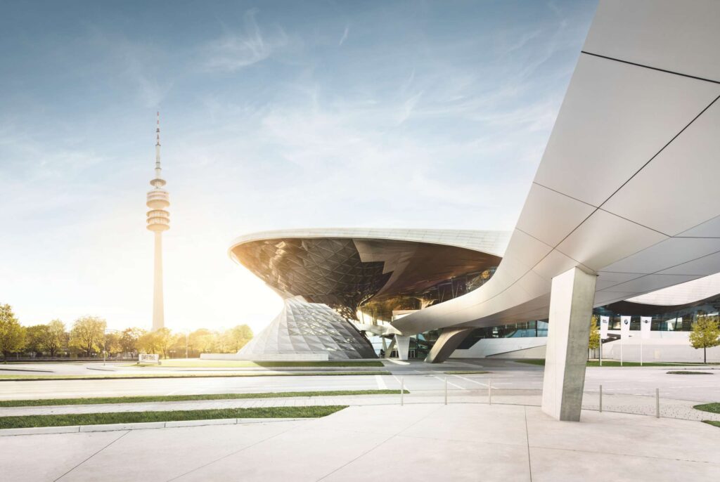
Looks like something out of a science fiction movie, eh?

You can find (Graphene Flagship spinoff companies), Emberion website here, BeDimensional website here, and Qurv Technologies website here.

7nm (nanometre) chip shakeup

From time to time I check out the latest on attempts to shrink computer chips. In my July 11, 2014 posting I noted IBM’s announcement about developing a 7nm computer chip and later in my July 15, 2015 posting I noted IBM’s announcement of a working 7nm chip (from a July 9, 2015 IBM news release , “The breakthrough, accomplished in partnership with GLOBALFOUNDRIES and Samsung at SUNY Polytechnic Institute’s Colleges of Nanoscale Science and Engineering (SUNY Poly CNSE), could result in the ability to place more than 20 billion tiny switches — transistors — on the fingernail-sized chips that power everything from smartphones to spacecraft.”

I’m not sure what happened to the IBM/Global Foundries/Samsung partnership but Global Foundries recently announced that it will no longer be working on 7nm chips. From an August 27, 2018 Global Foundries news release,

GLOBALFOUNDRIES [GF] today announced an important step in its transformation, continuing the trajectory launched with the appointment of Tom Caulfield as CEO earlier this year. In line with the strategic direction Caulfield has articulated, GF is reshaping its technology portfolio to intensify its focus on delivering truly differentiated offerings for clients in high-growth markets.

GF is realigning its leading-edge FinFET roadmap to serve the next wave of clients that will adopt the technology in the coming years. The company will shift development resources to make its 14/12nm FinFET platform more relevant to these clients, delivering a range of innovative IP and features including RF, embedded memory, low power and more. To support this transition, GF is putting its 7nm FinFET program on hold indefinitely [emphasis mine] and restructuring its research and development teams to support its enhanced portfolio initiatives. This will require a workforce reduction, however a significant number of top technologists will be redeployed on 14/12nm FinFET derivatives and other differentiated offerings.

I tried to find a definition for FinFet but the reference to a MOSFET and in-gate transistors was too much incomprehensible information packed into a tight space, see the FinFET Wikipedia entry for more, if you dare.

Getting back to the 7nm chip issue, Samuel K. Moore (I don’t think he’s related to the Moore of Moore’s law) wrote an Aug. 28, 2018 posting on the Nanoclast blog (on the IEEE [Institute of Electronics and Electrical Engineers] website) which provides some insight (Note: Links have been removed),

In a major shift in strategy, GlobalFoundries is halting its development of next-generation chipmaking processes. It had planned to move to the so-called 7-nm node, then begin to use extreme-ultraviolet lithography (EUV) to make that process cheaper. From there, it planned to develop even more advanced lithography that would allow for 5- and 3-nanometer nodes. Despite having installed at least one EUV machine at its Fab 8 facility in Malta, N.Y., all those plans are now on indefinite hold, the company announced Monday.

The move leaves only three companies reaching for the highest rungs of the Moore’s Law ladder: Intel, Samsung, and TSMC.

It’s a huge turnabout for GlobalFoundries. …

GlobalFoundries rationale for the move is that there are not enough customers that need bleeding-edge 7-nm processes to make it profitable. “While the leading edge gets most of the headlines, fewer customers can afford the transition to 7 nm and finer geometries,” said Samuel Wang, research vice president at Gartner, in a GlobalFoundries press release.

“The vast majority of today’s fabless [emphasis mine] customers are looking to get more value out of each technology generation to leverage the substantial investments required to design into each technology node,” explained GlobalFoundries CEO Tom Caulfield in a press release. “Essentially, these nodes are transitioning to design platforms serving multiple waves of applications, giving each node greater longevity. This industry dynamic has resulted in fewer fabless clients designing into the outer limits of Moore’s Law. We are shifting our resources and focus by doubling down on our investments in differentiated technologies across our entire portfolio that are most relevant to our clients in growing market segments.”

(The dynamic Caulfield describes is something the U.S. Defense Advanced Research Agency is working to disrupt with its $1.5-billion Electronics Resurgence Initiative. Darpa’s [DARPA] partners are trying to collapse the cost of design and allow older process nodes to keep improving by using 3D technology.)

Fabless manufacturing is where the fabrication is outsourced and the manufacturing company of record is focused on other matters according to the Fabless manufacturing Wikipedia entry.

Roland Moore-Colyer (I don’t think he’s related to Moore of Moore’s law either) has written August 28, 2018 article for theinquirer.net which also explores this latest news from Global Foundries (Note: Links have been removed),

EVER PREPPED A SPREAD for a party to then have less than half the people you were expecting show up? That’s probably how GlobalFoundries [sic] feels at the moment.

The chip manufacturer, which was once part of AMD, had a fabrication process geared up for 7-nanometre chips which its customers – including AMD and Qualcomm – were expected to adopt.

But AMD has confirmed that it’s decided to move its 7nm GPU production to TSMC, and Intel is still stuck trying to make chips based on 10nm fabrication.

Arguably, this could mark a stymieing of innovation and cutting-edge designs for chips in the near future. But with processors like AMD’s Threadripper 2990WX overclocked to run at 6GHz across all its 32 cores, in the real-world PC fans have no need to worry about consumer chips running out of puff anytime soon. µ

That’s all folks.

Maybe that’s not all

Steve Blank in a Sept. 10, 2018 posting on the Nanoclast blog (on the IEEE [Institute of Electrical and Electronics Engineers] website) provides some provocative commentary on the Global Foundries announcement (Note: A link has been removed),

For most of our lives, the idea that computers and technology would get better, faster, and cheaper every year was as assured as the sun rising every morning. The story “GlobalFoundries Halts 7-nm Chip Development”  doesn’t sound like the end of that era, but for you and anyone who uses an electronic device, it most certainly is.

Technology innovation is going to take a different direction.

This story just goes on and on

There was a new development according to a Sept. 12, 2018 posting on the Nanoclast blog by, again, Samuel K. Moore (Note Links have been removed),

At an event today [sept. 12, 2018], Apple executives said that the new iPhone Xs and Xs Max will contain the first smartphone processor to be made using 7 nm manufacturing technology, the most advanced process node. Huawei made the same claim, to less fanfare, late last month and it’s unclear who really deserves the accolades. If anybody does, it’s TSMC, which manufactures both chips.

TSMC went into volume production with 7-nm tech in April, and rival Samsung is moving toward commercial 7-nm production later this year or in early 2019. GlobalFoundries recently abandoned its attempts to develop a 7 nm process, reasoning that the multibillion-dollar investment would never pay for itself. And Intel announced delays in its move to its next manufacturing technology, which it calls a 10-nm node but which may be equivalent to others’ 7-nm technology.

There’s a certain ‘soap opera’ quality to this with all the twists and turns.

Aliens wreak havoc on our personal electronics

The aliens in question are subatomic particles and the havoc they wreak is low-grade according to the scientist who was presenting on the topic at the AAAS (American Association for the Advancement of Science) 2017 Annual Meeting (Feb. 16 – 20, 2017) in Boston, Massachusetts. From a Feb. 17, 2017 news item on ScienceDaily,

You may not realize it but alien subatomic particles raining down from outer space are wreaking low-grade havoc on your smartphones, computers and other personal electronic devices.

When your computer crashes and you get the dreaded blue screen or your smartphone freezes and you have to go through the time-consuming process of a reset, most likely you blame the manufacturer: Microsoft or Apple or Samsung. In many instances, however, these operational failures may be caused by the impact of electrically charged particles generated by cosmic rays that originate outside the solar system.

“This is a really big problem, but it is mostly invisible to the public,” said Bharat Bhuva, professor of electrical engineering at Vanderbilt University, in a presentation on Friday, Feb. 17 at a session titled “Cloudy with a Chance of Solar Flares: Quantifying the Risk of Space Weather” at the annual meeting of the American Association for the Advancement of Science in Boston.

A Feb. 17, 2017 Vanderbilt University news release (also on EurekAlert), which originated the news item, expands on  the theme,

When cosmic rays traveling at fractions of the speed of light strike the Earth’s atmosphere they create cascades of secondary particles including energetic neutrons, muons, pions and alpha particles. Millions of these particles strike your body each second. Despite their numbers, this subatomic torrent is imperceptible and has no known harmful effects on living organisms. However, a fraction of these particles carry enough energy to interfere with the operation of microelectronic circuitry. When they interact with integrated circuits, they may alter individual bits of data stored in memory. This is called a single-event upset or SEU.

Since it is difficult to know when and where these particles will strike and they do not do any physical damage, the malfunctions they cause are very difficult to characterize. As a result, determining the prevalence of SEUs is not easy or straightforward. “When you have a single bit flip, it could have any number of causes. It could be a software bug or a hardware flaw, for example. The only way you can determine that it is a single-event upset is by eliminating all the other possible causes,” Bhuva explained.

There have been a number of incidents that illustrate how serious the problem can be, Bhuva reported. For example, in 2003 in the town of Schaerbeek, Belgium a bit flip in an electronic voting machine added 4,096 extra votes to one candidate. The error was only detected because it gave the candidate more votes than were possible and it was traced to a single bit flip in the machine’s register. In 2008, the avionics system of a Qantus passenger jet flying from Singapore to Perth appeared to suffer from a single-event upset that caused the autopilot to disengage. As a result, the aircraft dove 690 feet in only 23 seconds, injuring about a third of the passengers seriously enough to cause the aircraft to divert to the nearest airstrip. In addition, there have been a number of unexplained glitches in airline computers – some of which experts feel must have been caused by SEUs – that have resulted in cancellation of hundreds of flights resulting in significant economic losses.

An analysis of SEU failure rates for consumer electronic devices performed by Ritesh Mastipuram and Edwin Wee at Cypress Semiconductor on a previous generation of technology shows how prevalent the problem may be. Their results were published in 2004 in Electronic Design News and provided the following estimates:

  • A simple cell phone with 500 kilobytes of memory should only have one potential error every 28 years.
  • A router farm like those used by Internet providers with only 25 gigabytes of memory may experience one potential networking error that interrupts their operation every 17 hours.
  • A person flying in an airplane at 35,000 feet (where radiation levels are considerably higher than they are at sea level) who is working on a laptop with 500 kilobytes of memory may experience one potential error every five hours.

Bhuva is a member of Vanderbilt’s Radiation Effects Research Group, which was established in 1987 and is the largest academic program in the United States that studies the effects of radiation on electronic systems. The group’s primary focus was on military and space applications. Since 2001, the group has also been analyzing radiation effects on consumer electronics in the terrestrial environment. They have studied this phenomenon in the last eight generations of computer chip technology, including the current generation that uses 3D transistors (known as FinFET) that are only 16 nanometers in size. The 16-nanometer study was funded by a group of top microelectronics companies, including Altera, ARM, AMD, Broadcom, Cisco Systems, Marvell, MediaTek, Renesas, Qualcomm, Synopsys, and TSMC

“The semiconductor manufacturers are very concerned about this problem because it is getting more serious as the size of the transistors in computer chips shrink and the power and capacity of our digital systems increase,” Bhuva said. “In addition, microelectronic circuits are everywhere and our society is becoming increasingly dependent on them.”

To determine the rate of SEUs in 16-nanometer chips, the Vanderbilt researchers took samples of the integrated circuits to the Irradiation of Chips and Electronics (ICE) House at Los Alamos National Laboratory. There they exposed them to a neutron beam and analyzed how many SEUs the chips experienced. Experts measure the failure rate of microelectronic circuits in a unit called a FIT, which stands for failure in time. One FIT is one failure per transistor in one billion hours of operation. That may seem infinitesimal but it adds up extremely quickly with billions of transistors in many of our devices and billions of electronic systems in use today (the number of smartphones alone is in the billions). Most electronic components have failure rates measured in 100’s and 1,000’s of FITs.

chart

Trends in single event upset failure rates at the individual transistor, integrated circuit and system or device level for the three most recent manufacturing technologies. (Bharat Bhuva, Radiation Effects Research Group, Vanderbilt University)

“Our study confirms that this is a serious and growing problem,” said Bhuva.“This did not come as a surprise. Through our research on radiation effects on electronic circuits developed for military and space applications, we have been anticipating such effects on electronic systems operating in the terrestrial environment.”

Although the details of the Vanderbilt studies are proprietary, Bhuva described the general trend that they have found in the last three generations of integrated circuit technology: 28-nanometer, 20-nanometer and 16-nanometer.

As transistor sizes have shrunk, they have required less and less electrical charge to represent a logical bit. So the likelihood that one bit will “flip” from 0 to 1 (or 1 to 0) when struck by an energetic particle has been increasing. This has been partially offset by the fact that as the transistors have gotten smaller they have become smaller targets so the rate at which they are struck has decreased.

More significantly, the current generation of 16-nanometer circuits have a 3D architecture that replaced the previous 2D architecture and has proven to be significantly less susceptible to SEUs. Although this improvement has been offset by the increase in the number of transistors in each chip, the failure rate at the chip level has also dropped slightly. However, the increase in the total number of transistors being used in new electronic systems has meant that the SEU failure rate at the device level has continued to rise.

Unfortunately, it is not practical to simply shield microelectronics from these energetic particles. For example, it would take more than 10 feet of concrete to keep a circuit from being zapped by energetic neutrons. However, there are ways to design computer chips to dramatically reduce their vulnerability.

For cases where reliability is absolutely critical, you can simply design the processors in triplicate and have them vote. Bhuva pointed out: “The probability that SEUs will occur in two of the circuits at the same time is vanishingly small. So if two circuits produce the same result it should be correct.” This is the approach that NASA used to maximize the reliability of spacecraft computer systems.

The good news, Bhuva said, is that the aviation, medical equipment, IT, transportation, communications, financial and power industries are all aware of the problem and are taking steps to address it. “It is only the consumer electronics sector that has been lagging behind in addressing this problem.”

The engineer’s bottom line: “This is a major problem for industry and engineers, but it isn’t something that members of the general public need to worry much about.”

That’s fascinating and I hope the consumer electronics industry catches up with this ‘alien invasion’ issue. Finally, the ‘bit flips’ made me think of the 1956 movie ‘Invasion of the Body Snatchers‘.