Tag Archives: artificial neural network

Analogue memristor for next-generation brain-mimicking (neuromorphic) computing

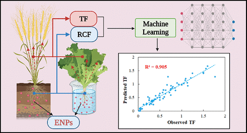
This research into an analogue memristor comes from The Korea Institute of Science and Technology (KIST) according to a September 20, 2022 news item on Nanowerk, Note: A link has been removed,

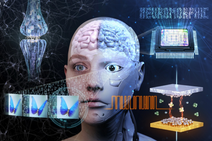
Neuromorphic computing system technology mimicking the human brain has emerged and overcome the limitation of excessive power consumption regarding the existing von Neumann computing method. A high-performance, analog artificial synapse device, capable of expressing various synapse connection strengths, is required to implement a semiconductor device that uses a brain information transmission method. This method uses signals transmitted between neurons when a neuron generates a spike signal.

However, considering conventional resistance-variable memory devices widely used as artificial synapses, as the filament grows with varying resistance, the electric field increases, causing a feedback phenomenon, resulting in rapid filament growth. Therefore, it is challenging to implement considerable plasticity while maintaining analog (gradual) resistance variation concerning the filament type.

The Korea Institute of Science and Technology (KIST), led by Dr. YeonJoo Jeong’s team at the Center for Neuromorphic Engineering, solved the limitations of analog synaptic characteristics, plasticity and information preservation, which are chronic obstacles regarding memristors, neuromorphic semiconductor devices. He announced the development of an artificial synaptic semiconductor device capable of highly reliable neuromorphic computing (Nature Communications, “Cluster-type analogue memristor by engineering redox dynamics for high-performance neuromorphic computing”).

Caption: Concept image of the article Credit: Korea Institute of Science and Technology (KIST)

A September 20, 2022 (Korea) National Research Council of Science & Technology press release on EurekAlert, which originated the news item, delves further into the research,

The KIST research team fine-tuned the redox properties of active electrode ions to solve small synaptic plasticity hindering the performance of existing neuromorphic semiconductor devices. Furthermore, various transition metals were doped and used in the synaptic device, controlling the reduction probability of active electrode ions. It was discovered that the high reduction probability of ions is a critical variable in the development of high-performance artificial synaptic devices.

Therefore, a titanium transition metal, having a high ion reduction probability, was introduced by the research team into an existing artificial synaptic device. This maintains the synapse’s analog characteristics and the device plasticity at the synapse of the biological brain, approximately five times the difference between high and low resistances. Furthermore, they developed a high-performance neuromorphic semiconductor that is approximately 50 times more efficient.

Additionally, due to the high alloy formation reaction concerning the doped titanium transition metal, the information retention increased up to 63 times compared with the existing artificial synaptic device. Furthermore, brain functions, including long-term potentiation and long-term depression, could be more precisely simulated.

The team implemented an artificial neural network learning pattern using the developed artificial synaptic device and attempted artificial intelligence image recognition learning. As a result, the error rate was reduced by more than 60% compared with the existing artificial synaptic device; additionally, the handwriting image pattern (MNIST) recognition accuracy increased by more than 69%. The research team confirmed the feasibility of a high-performance neuromorphic computing system through this improved the artificial synaptic device.

Dr. Jeong of KIST stated, “This study drastically improved the synaptic range of motion and information preservation, which were the greatest technical barriers of existing synaptic mimics.” “In the developed artificial synapse device, the device’s analog operation area to express the synapse’s various connection strengths has been maximized, so the performance of brain simulation-based artificial intelligence computing will be improved.” Additionally, he mentioned, “In the follow-up research, we will manufacture a neuromorphic semiconductor chip based on the developed artificial synapse device to realize a high-performance artificial intelligence system, thereby further enhancing competitiveness in the domestic system and artificial intelligence semiconductor field.”

Here’s a link to and a citation for the paper,

Cluster-type analogue memristor by engineering redox dynamics for high-performance neuromorphic computing by Jaehyun Kang, Taeyoon Kim, Suman Hu, Jaewook Kim, Joon Young Kwak, Jongkil Park, Jong Keuk Park, Inho Kim, Suyoun Lee, Sangbum Kim & YeonJoo Jeong. Nature Communications volume 13, Article number: 4040 (2022) DOI: https://doi.org/10.1038/s41467-022-31804-4 Published: 12 July 2022

This paper is open access.

Use AI to reduce worries about nanoparticles in food

A June 16, 2021 news item on ScienceDaily announces research into the impact that engineered metallic nanoparticles used in agricultural practices have on food,

While crop yield has achieved a substantial boost from nanotechnology in recent years, alarms over the health risks posed by nanoparticles within fresh produce and grains have also increased. In particular, nanoparticles entering the soil through irrigation, fertilizers and other sources have raised concerns about whether plants absorb these minute particles enough to cause toxicity.

In a new study published online in the journal Environmental Science and Technology, researchers at Texas A&M University have used machine learning [a form of artificial intelligence {AI}] to evaluate the salient properties of metallic nanoparticles that make them more susceptible for plant uptake. The researchers said their algorithm could indicate how much plants accumulate nanoparticles in their roots and shoots.

A June 16, 2021 Texas A&M University news release (also on EurekAlert), which originated the news item, describes the research, which employed two different machine learning algorithms, in more detail,

Nanoparticles are a burgeoning trend in several fields, including medicine, consumer products and agriculture. Depending on the type of nanoparticle, some have favorable surface properties, charge and magnetism, among other features. These qualities make them ideal for a number of applications. For example, in agriculture, nanoparticles may be used as antimicrobials to protect plants from pathogens. Alternatively, they can be used to bind to fertilizers or insecticides and then programmed for slow release to increase plant absorption.

These agricultural practices and others, like irrigation, can cause nanoparticles to accumulate in the soil. However, with the different types of nanoparticles that could exist in the ground and a staggeringly large number of terrestrial plant species, including food crops, it is not clearly known if certain properties of nanoparticles make them more likely to be absorbed by some plant species than others.

“As you can imagine, if we have to test the presence of each nanoparticle for every plant species, it is a huge number of experiments, which is very time-consuming and expensive,” said Xingmao “Samuel” Ma, associate professor in the Zachry Department of Civil and Environmental Engineering. “To give you an idea, silver nanoparticles alone can have hundreds of different sizes, shapes and surface coatings, and so, experimentally testing each one, even for a single plant species, is impractical.”

Instead, for their study, the researchers chose two different machine learning algorithms, an artificial neural network and gene-expression programming. They first trained these algorithms on a database created from past research on different metallic nanoparticles and the specific plants in which they accumulated. In particular, their database contained the size, shape and other characteristics of different nanoparticles, along with information on how much of these particles were absorbed from soil or nutrient-enriched water into the plant body.

Once trained, their machine learning algorithms could correctly predict the likelihood of a given metallic nanoparticle to accumulate in a plant species. Also, their algorithms revealed that when plants are in a nutrient-enriched or hydroponic solution, the chemical makeup of the metallic nanoparticle determines the propensity of accumulation in the roots and shoots. But if plants are grown in soil, the contents of organic matter and the clay in soil are key to nanoparticle uptake.

Ma said that while the machine learning algorithms could make predictions for most food crops and terrestrial plants, they might not yet be ready for aquatic plants. He also noted that the next step in his research would be to investigate if the machine learning algorithms could predict nanoparticle uptake from leaves rather than through the roots.

“It is quite understandable that people are concerned about the presence of nanoparticles in their fruits, vegetables and grains,” said Ma. “But instead of not using nanotechnology altogether, we would like farmers to reap the many benefits provided by this technology but avoid the potential food safety concerns.”

This image accompanies the paper’s research abstract,

[downloaded frm https://pubs.acs.org/doi/full/10.1021/acs.est.1c01603]

Here’s a link to and a citation for the paper,

Prediction of Plant Uptake and Translocation of Engineered Metallic Nanoparticles by Machine Learning by Xiaoxuan Wang, Liwei Liu, Weilan Zhang, and Xingmao Ma. Environ. Sci. Technol. 2021, 55, 11, 7491–7500 DOI: https://doi.org/10.1021/acs.est.1c01603 Publication Date:May 17, 2021 Copyright © 2021 American Chemical Society

This paper is behind a paywall.

New path to viable memristor/neuristor?

I first stumbled onto memristors and the possibility of brain-like computing sometime in 2008 (around the time that R. Stanley Williams and his team at HP Labs first published the results of their research linking Dr. Leon Chua’s memristor theory to their attempts to shrink computer chips). In the almost 10 years since, scientists have worked hard to utilize memristors in the field of neuromorphic (brain-like) engineering/computing.

A January 22, 2018 news item on phys.org describes the latest work,

When it comes to processing power, the human brain just can’t be beat.

Packed within the squishy, football-sized organ are somewhere around 100 billion neurons. At any given moment, a single neuron can relay instructions to thousands of other neurons via synapses—the spaces between neurons, across which neurotransmitters are exchanged. There are more than 100 trillion synapses that mediate neuron signaling in the brain, strengthening some connections while pruning others, in a process that enables the brain to recognize patterns, remember facts, and carry out other learning tasks, at lightning speeds.

Researchers in the emerging field of “neuromorphic computing” have attempted to design computer chips that work like the human brain. Instead of carrying out computations based on binary, on/off signaling, like digital chips do today, the elements of a “brain on a chip” would work in an analog fashion, exchanging a gradient of signals, or “weights,” much like neurons that activate in various ways depending on the type and number of ions that flow across a synapse.

In this way, small neuromorphic chips could, like the brain, efficiently process millions of streams of parallel computations that are currently only possible with large banks of supercomputers. But one significant hangup on the way to such portable artificial intelligence has been the neural synapse, which has been particularly tricky to reproduce in hardware.

Now engineers at MIT [Massachusetts Institute of Technology] have designed an artificial synapse in such a way that they can precisely control the strength of an electric current flowing across it, similar to the way ions flow between neurons. The team has built a small chip with artificial synapses, made from silicon germanium. In simulations, the researchers found that the chip and its synapses could be used to recognize samples of handwriting, with 95 percent accuracy.

A January 22, 2018 MIT news release by Jennifer Chua (also on EurekAlert), which originated the news item, provides more detail about the research,

The design, published today [January 22, 2018] in the journal Nature Materials, is a major step toward building portable, low-power neuromorphic chips for use in pattern recognition and other learning tasks.

The research was led by Jeehwan Kim, the Class of 1947 Career Development Assistant Professor in the departments of Mechanical Engineering and Materials Science and Engineering, and a principal investigator in MIT’s Research Laboratory of Electronics and Microsystems Technology Laboratories. His co-authors are Shinhyun Choi (first author), Scott Tan (co-first author), Zefan Li, Yunjo Kim, Chanyeol Choi, and Hanwool Yeon of MIT, along with Pai-Yu Chen and Shimeng Yu of Arizona State University.

Too many paths

Most neuromorphic chip designs attempt to emulate the synaptic connection between neurons using two conductive layers separated by a “switching medium,” or synapse-like space. When a voltage is applied, ions should move in the switching medium to create conductive filaments, similarly to how the “weight” of a synapse changes.

But it’s been difficult to control the flow of ions in existing designs. Kim says that’s because most switching mediums, made of amorphous materials, have unlimited possible paths through which ions can travel — a bit like Pachinko, a mechanical arcade game that funnels small steel balls down through a series of pins and levers, which act to either divert or direct the balls out of the machine.

Like Pachinko, existing switching mediums contain multiple paths that make it difficult to predict where ions will make it through. Kim says that can create unwanted nonuniformity in a synapse’s performance.

“Once you apply some voltage to represent some data with your artificial neuron, you have to erase and be able to write it again in the exact same way,” Kim says. “But in an amorphous solid, when you write again, the ions go in different directions because there are lots of defects. This stream is changing, and it’s hard to control. That’s the biggest problem — nonuniformity of the artificial synapse.”

A perfect mismatch

Instead of using amorphous materials as an artificial synapse, Kim and his colleagues looked to single-crystalline silicon, a defect-free conducting material made from atoms arranged in a continuously ordered alignment. The team sought to create a precise, one-dimensional line defect, or dislocation, through the silicon, through which ions could predictably flow.

To do so, the researchers started with a wafer of silicon, resembling, at microscopic resolution, a chicken-wire pattern. They then grew a similar pattern of silicon germanium — a material also used commonly in transistors — on top of the silicon wafer. Silicon germanium’s lattice is slightly larger than that of silicon, and Kim found that together, the two perfectly mismatched materials can form a funnel-like dislocation, creating a single path through which ions can flow.

The researchers fabricated a neuromorphic chip consisting of artificial synapses made from silicon germanium, each synapse measuring about 25 nanometers across. They applied voltage to each synapse and found that all synapses exhibited more or less the same current, or flow of ions, with about a 4 percent variation between synapses — a much more uniform performance compared with synapses made from amorphous material.

They also tested a single synapse over multiple trials, applying the same voltage over 700 cycles, and found the synapse exhibited the same current, with just 1 percent variation from cycle to cycle.

“This is the most uniform device we could achieve, which is the key to demonstrating artificial neural networks,” Kim says.

Writing, recognized

As a final test, Kim’s team explored how its device would perform if it were to carry out actual learning tasks — specifically, recognizing samples of handwriting, which researchers consider to be a first practical test for neuromorphic chips. Such chips would consist of “input/hidden/output neurons,” each connected to other “neurons” via filament-based artificial synapses.

Scientists believe such stacks of neural nets can be made to “learn.” For instance, when fed an input that is a handwritten ‘1,’ with an output that labels it as ‘1,’ certain output neurons will be activated by input neurons and weights from an artificial synapse. When more examples of handwritten ‘1s’ are fed into the same chip, the same output neurons may be activated when they sense similar features between different samples of the same letter, thus “learning” in a fashion similar to what the brain does.

Kim and his colleagues ran a computer simulation of an artificial neural network consisting of three sheets of neural layers connected via two layers of artificial synapses, the properties of which they based on measurements from their actual neuromorphic chip. They fed into their simulation tens of thousands of samples from a handwritten recognition dataset commonly used by neuromorphic designers, and found that their neural network hardware recognized handwritten samples 95 percent of the time, compared to the 97 percent accuracy of existing software algorithms.

The team is in the process of fabricating a working neuromorphic chip that can carry out handwriting-recognition tasks, not in simulation but in reality. Looking beyond handwriting, Kim says the team’s artificial synapse design will enable much smaller, portable neural network devices that can perform complex computations that currently are only possible with large supercomputers.

“Ultimately we want a chip as big as a fingernail to replace one big supercomputer,” Kim says. “This opens a stepping stone to produce real artificial hardware.”

This research was supported in part by the National Science Foundation.

Here’s a link to and a citation for the paper,

SiGe epitaxial memory for neuromorphic computing with reproducible high performance based on engineered dislocations by Shinhyun Choi, Scott H. Tan, Zefan Li, Yunjo Kim, Chanyeol Choi, Pai-Yu Chen, Hanwool Yeon, Shimeng Yu, & Jeehwan Kim. Nature Materials (2018) doi:10.1038/s41563-017-0001-5 Published online: 22 January 2018

This paper is behind a paywall.

For the curious I have included a number of links to recent ‘memristor’ postings here,

January 22, 2018: Memristors at Masdar

January 3, 2018: Mott memristor

August 24, 2017: Neuristors and brainlike computing

June 28, 2017: Dr. Wei Lu and bio-inspired ‘memristor’ chips

May 2, 2017: Predicting how a memristor functions

December 30, 2016: Changing synaptic connectivity with a memristor

December 5, 2016: The memristor as computing device

November 1, 2016: The memristor as the ‘missing link’ in bioelectronic medicine?

You can find more by using ‘memristor’ as the search term in the blog search function or on the search engine of your choice.

Spintronics-based artificial intelligence

Courtesy: Tohoku University

Japanese researchers have managed to mimic a synapse (artificial neural network) with a spintronics-based device according to a Dec. 19, 2016 Tohoku University press release (also on EurekAlert but dated Dec. 20, 2016),

Researchers at Tohoku University have, for the first time, successfully demonstrated the basic operation of spintronics-based artificial intelligence.

Artificial intelligence, which emulates the information processing function of the brain that can quickly execute complex and complicated tasks such as image recognition and weather prediction, has attracted growing attention and has already been partly put to practical use.

The currently-used artificial intelligence works on the conventional framework of semiconductor-based integrated circuit technology. However, this lacks the compactness and low-power feature of the human brain. To overcome this challenge, the implementation of a single solid-state device that plays the role of a synapse is highly promising.

The Tohoku University research group of Professor Hideo Ohno, Professor Shigeo Sato, Professor Yoshihiko Horio, Associate Professor Shunsuke Fukami and Assistant Professor Hisanao Akima developed an artificial neural network in which their recently-developed spintronic devices, comprising micro-scale magnetic material, are employed (Fig. 1). The used spintronic device is capable of memorizing arbitral values between 0 and 1 in an analogue manner unlike the conventional magnetic devices, and thus perform the learning function, which is served by synapses in the brain.

Using the developed network (Fig. 2), the researchers examined an associative memory operation, which is not readily executed by conventional computers. Through the multiple trials, they confirmed that the spintronic devices have a learning ability with which the developed artificial neural network can successfully associate memorized patterns (Fig. 3) from their input noisy versions just like the human brain can.

The proof-of-concept demonstration in this research is expected to open new horizons in artificial intelligence technology – one which is of a compact size, and which simultaneously achieves fast-processing capabilities and ultralow-power consumption. These features should enable the artificial intelligence to be used in a broad range of societal applications such as image/voice recognition, wearable terminals, sensor networks and nursing-care robots.

Here are Fig. 1 and Fig. 2, as mentioned in the press release,

Fig. 1. (a) Optical photograph of a fabricated spintronic device that serves as artificial synapse in the present demonstration. Measurement circuit for the resistance switching is also shown. (b) Measured relation between the resistance of the device and applied current, showing analogue-like resistance variation. (c) Photograph of spintronic device array mounted on a ceramic package, which is used for the developed artificial neural network. Courtesy: Tohoku University

Fig. 2. Block diagram of developed artificial neural network, consisting of PC, FPGA, and array of spintronics (spin-orbit torque; SOT) devices. Courtesy: Tohoku University

Here`s a link to and a citation for the paper,

Analogue spin–orbit torque device for artificial-neural-network-based associative memory operation by William A. Borders, Hisanao Akima1, Shunsuke Fukami, Satoshi Moriya, Shouta Kurihara, Yoshihiko Horio, Shigeo Sato, and Hideo Ohno. Applied Physics Express, Volume 10, Number 1 https://doi.org/10.7567/APEX.10.013007. Published 20 December 2016

© 2017 The Japan Society of Applied Physics

This is an open access paper.

For anyone interested in my other posts on memristors, artificial brains, and artificial intelligence, you can search this blog for those terms  and/or Neuromorphic Engineering in the Categories section.

Artificial synapse rivals biological synapse in energy consumption

How can we make computers be like biological brains which do so much work and use so little power? It’s a question scientists from many countries are trying to answer and it seems South Korean scientists are proposing an answer. From a June 20, 2016 news item on Nanowerk,

News) Creation of an artificial intelligence system that fully emulates the functions of a human brain has long been a dream of scientists. A brain has many superior functions as compared with super computers, even though it has light weight, small volume, and consumes extremely low energy. This is required to construct an artificial neural network, in which a huge amount (1014)) of synapses is needed.

Most recently, great efforts have been made to realize synaptic functions in single electronic devices, such as using resistive random access memory (RRAM), phase change memory (PCM), conductive bridges, and synaptic transistors. Artificial synapses based on highly aligned nanostructures are still desired for the construction of a highly-integrated artificial neural network.

Prof. Tae-Woo Lee, research professor Wentao Xu, and Dr. Sung-Yong Min with the Dept. of Materials Science and Engineering at POSTECH [Pohang University of Science & Technology, South Korea] have succeeded in fabricating an organic nanofiber (ONF) electronic device that emulates not only the important working principles and energy consumption of biological synapses but also the morphology. …

A June 20, 2016 Pohang University of Science & Technology (POSTECH) news release on EurekAlert, which originated the news item, describes the work in more detail,

The morphology of ONFs is very similar to that of nerve fibers, which form crisscrossing grids to enable the high memory density of a human brain. Especially, based on the e-Nanowire printing technique, highly-aligned ONFs can be massively produced with precise control over alignment and dimension. This morphology potentially enables the future construction of high-density memory of a neuromorphic system.

Important working principles of a biological synapse have been emulated, such as paired-pulse facilitation (PPF), short-term plasticity (STP), long-term plasticity (LTP), spike-timing dependent plasticity (STDP), and spike-rate dependent plasticity (SRDP). Most amazingly, energy consumption of the device can be reduced to a femtojoule level per synaptic event, which is a value magnitudes lower than previous reports. It rivals that of a biological synapse. In addition, the organic artificial synapse devices not only provide a new research direction in neuromorphic electronics but even open a new era of organic electronics.

This technology will lead to the leap of brain-inspired electronics in both memory density and energy consumption aspects. The artificial synapse developed by Prof. Lee’s research team will provide important potential applications to neuromorphic computing systems and artificial intelligence systems for autonomous cars (or self-driving cars), analysis of big data, cognitive systems, robot control, medical diagnosis, stock trading analysis, remote sensing, and other smart human-interactive systems and machines in the future.

Here’s a link to and a citation for the paper,

Organic core-sheath nanowire artificial synapses with femtojoule energy consumption by Wentao Xu, Sung-Yong Min, Hyunsang Hwang, and Tae-Woo Lee. Science Advances  17 Jun 2016: Vol. 2, no. 6, e1501326 DOI: 10.1126/sciadv.1501326

This paper is open access.