This research into an analogue memristor comes from The Korea Institute of Science and Technology (KIST) according to a September 20, 2022 news item on Nanowerk, Note: A link has been removed,
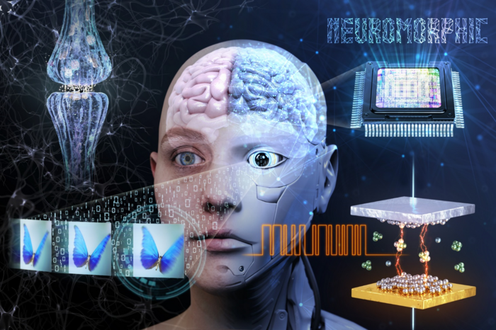
Neuromorphic computing system technology mimicking the human brain has emerged and overcome the limitation of excessive power consumption regarding the existing von Neumann computing method. A high-performance, analog artificial synapse device, capable of expressing various synapse connection strengths, is required to implement a semiconductor device that uses a brain information transmission method. This method uses signals transmitted between neurons when a neuron generates a spike signal.
However, considering conventional resistance-variable memory devices widely used as artificial synapses, as the filament grows with varying resistance, the electric field increases, causing a feedback phenomenon, resulting in rapid filament growth. Therefore, it is challenging to implement considerable plasticity while maintaining analog (gradual) resistance variation concerning the filament type.
The Korea Institute of Science and Technology (KIST), led by Dr. YeonJoo Jeong’s team at the Center for Neuromorphic Engineering, solved the limitations of analog synaptic characteristics, plasticity and information preservation, which are chronic obstacles regarding memristors, neuromorphic semiconductor devices. He announced the development of an artificial synaptic semiconductor device capable of highly reliable neuromorphic computing (Nature Communications, “Cluster-type analogue memristor by engineering redox dynamics for high-performance neuromorphic computing”).
…
Caption: Concept image of the article Credit: Korea Institute of Science and Technology (KIST)
The KIST research team fine-tuned the redox properties of active electrode ions to solve small synaptic plasticity hindering the performance of existing neuromorphic semiconductor devices. Furthermore, various transition metals were doped and used in the synaptic device, controlling the reduction probability of active electrode ions. It was discovered that the high reduction probability of ions is a critical variable in the development of high-performance artificial synaptic devices.
Therefore, a titanium transition metal, having a high ion reduction probability, was introduced by the research team into an existing artificial synaptic device. This maintains the synapse’s analog characteristics and the device plasticity at the synapse of the biological brain, approximately five times the difference between high and low resistances. Furthermore, they developed a high-performance neuromorphic semiconductor that is approximately 50 times more efficient.
Additionally, due to the high alloy formation reaction concerning the doped titanium transition metal, the information retention increased up to 63 times compared with the existing artificial synaptic device. Furthermore, brain functions, including long-term potentiation and long-term depression, could be more precisely simulated.
The team implemented an artificial neural network learning pattern using the developed artificial synaptic device and attempted artificial intelligence image recognition learning. As a result, the error rate was reduced by more than 60% compared with the existing artificial synaptic device; additionally, the handwriting image pattern (MNIST) recognition accuracy increased by more than 69%. The research team confirmed the feasibility of a high-performance neuromorphic computing system through this improved the artificial synaptic device.
Dr. Jeong of KIST stated, “This study drastically improved the synaptic range of motion and information preservation, which were the greatest technical barriers of existing synaptic mimics.” “In the developed artificial synapse device, the device’s analog operation area to express the synapse’s various connection strengths has been maximized, so the performance of brain simulation-based artificial intelligence computing will be improved.” Additionally, he mentioned, “In the follow-up research, we will manufacture a neuromorphic semiconductor chip based on the developed artificial synapse device to realize a high-performance artificial intelligence system, thereby further enhancing competitiveness in the domestic system and artificial intelligence semiconductor field.”
The word ‘memristor’ usually pops up when there’s research into artificial synapses but not in this new piece of research. I didn’t see any mention of the memristor in the paper’s references either but I did find James Gimzewski from the University of California at Los Angeles (UCLA) whose research into brainlike computing (neuromorphic computing) is running parallel but separately to the memristor research.
Dr. Thamarasee Jeewandara has written a March 25, 2021 article for phys.org about the latest neuromorphic computing research (Note: Links have been removed)
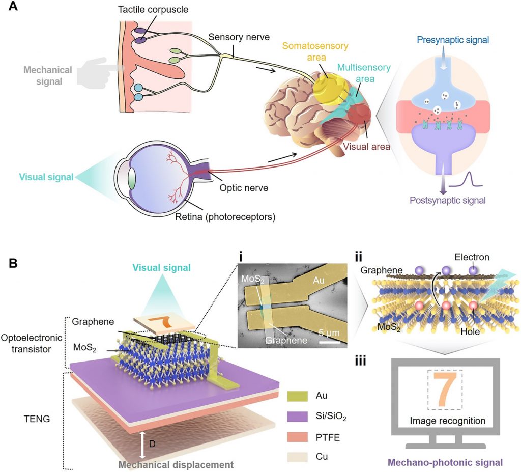
Multifunctional and diverse artificial neural systems can incorporate multimodal plasticity, memory and supervised learning functions to assist neuromorphic computation. In a new report, Jinran Yu and a research team in nanoenergy, nanoscience and materials science in China and the US., presented a bioinspired mechano-photonic artificial synapse with synergistic mechanical and optical plasticity. The team used an optoelectronic transistor made of graphene/molybdenum disulphide (MoS2) heterostructure and an integrated triboelectric nanogenerator to compose the artificial synapse. They controlled the charge transfer/exchange in the heterostructure with triboelectric potential and modulated the optoelectronic synapse behaviors readily, including postsynaptic photocurrents, photosensitivity and photoconductivity. The mechano-photonic artificial synapse is a promising implementation to mimic the complex biological nervous system and promote the development of interactive artificial intelligence. The work is now published on Science Advances.
…
The human brain can integrate cognition, learning and memory tasks via auditory, visual, olfactory and somatosensory interactions. This process is difficult to be mimicked using conventional von Neumann architectures that require additional sophisticated functions. Brain-inspired neural networks are made of various synaptic devices to transmit information and process using the synaptic weight. Emerging photonic synapse combine the optical and electric neuromorphic modulation and computation to offer a favorable option with high bandwidth, fast speed and low cross-talk to significantly reduce power consumption. Biomechanical motions including touch, eye blinking and arm waving are other ubiquitous triggers or interactive signals to operate electronics during artificial synapse plasticization. In this work, Yu et al. presented a mechano-photonic artificial synapse with synergistic mechanical and optical plasticity. The device contained an optoelectronic transistor and an integrated triboelectric nanogenerator (TENG) in contact-separation mode. The mechano-optical artificial synapses have huge functional potential as interactive optoelectronic interfaces, synthetic retinas and intelligent robots. [emphasis mine]
…
As you can see Jeewandara has written quite a technical summary of the work. Here’s an image from the Science Advances paper,
Fig. 1 Biological tactile/visual neurons and mechano-photonic artificial synapse.
(A) Schematic illustrations of biological tactile/visual sensory system. (B) Schematic diagram of the mechano-photonic artificial synapse based on graphene/MoS2 (Gr/MoS2) heterostructure. (i) Top-view scanning electron microscope (SEM) image of the optoelectronic transistor; scale bar, 5 μm. The cyan area indicates the MoS2 flake, while the white strip is graphene. (ii) Illustration of charge transfer/exchange for Gr/MoS2 heterostructure. (iii) Output mechano-photonic signals from the artificial synapse for image recognition.
This is the second neuromorphic computing chip story from MIT this summer in what has turned out to be a bumper crop of research announcements in this field. The first MIT synapse story was featured in a June 16, 2020 posting. Now, there’s a second and completely different team announcing results for their artificial brain synapse work in a June 19, 2020 news item on Nanowerk (Note: A link has been removed),
Teams around the world are building ever more sophisticated artificial intelligence systems of a type called neural networks, designed in some ways to mimic the wiring of the brain, for carrying out tasks such as computer vision and natural language processing.
Using state-of-the-art semiconductor circuits to simulate neural networks requires large amounts of memory and high power consumption. Now, an MIT [Massachusetts Institute of Technology] team has made strides toward an alternative system, which uses physical, analog devices that can much more efficiently mimic brain processes.
The findings are described in the journal Nature Communications (“Protonic solid-state electrochemical synapse for physical neural networks”), in a paper by MIT professors Bilge Yildiz, Ju Li, and Jesús del Alamo, and nine others at MIT and Brookhaven National Laboratory. The first author of the paper is Xiahui Yao, a former MIT postdoc now working on energy storage at GRU Energy Lab.
That description of the work is one pretty much every team working on developing memristive (neuromorphic) chips could use.
On other fronts, the team has produced a very attractive illustration accompanying this research (aside: Is it my imagination or has there been a serious investment in the colour pink and other pastels for science illustrations?),
A new system developed at MIT and Brookhaven National Lab could provide a faster, more reliable and much more energy efficient approach to physical neural networks, by using analog ionic-electronic devices to mimic synapses.. Courtesy of the researchers
A June 19, 2020 MIT news release, which originated the news item, provides more insight into this specific piece of research (hint: it’s about energy use and repeatability),
Neural networks attempt to simulate the way learning takes place in the brain, which is based on the gradual strengthening or weakening of the connections between neurons, known as synapses. The core component of this physical neural network is the resistive switch, whose electronic conductance can be controlled electrically. This control, or modulation, emulates the strengthening and weakening of synapses in the brain.
In neural networks using conventional silicon microchip technology, the simulation of these synapses is a very energy-intensive process. To improve efficiency and enable more ambitious neural network goals, researchers in recent years have been exploring a number of physical devices that could more directly mimic the way synapses gradually strengthen and weaken during learning and forgetting.
Most candidate analog resistive devices so far for such simulated synapses have either been very inefficient, in terms of energy use, or performed inconsistently from one device to another or one cycle to the next. The new system, the researchers say, overcomes both of these challenges. “We’re addressing not only the energy challenge, but also the repeatability-related challenge that is pervasive in some of the existing concepts out there,” says Yildiz, who is a professor of nuclear science and engineering and of materials science and engineering.
“I think the bottleneck today for building [neural network] applications is energy efficiency. It just takes too much energy to train these systems, particularly for applications on the edge, like autonomous cars,” says del Alamo, who is the Donner Professor in the Department of Electrical Engineering and Computer Science. Many such demanding applications are simply not feasible with today’s technology, he adds.
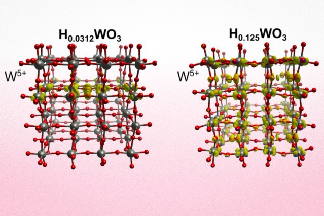
The resistive switch in this work is an electrochemical device, which is made of tungsten trioxide (WO3) and works in a way similar to the charging and discharging of batteries. Ions, in this case protons, can migrate into or out of the crystalline lattice of the material, explains Yildiz, depending on the polarity and strength of an applied voltage. These changes remain in place until altered by a reverse applied voltage — just as the strengthening or weakening of synapses does.
The mechanism is similar to the doping of semiconductors,” says Li, who is also a professor of nuclear science and engineering and of materials science and engineering. In that process, the conductivity of silicon can be changed by many orders of magnitude by introducing foreign ions into the silicon lattice. “Traditionally those ions were implanted at the factory,” he says, but with the new device, the ions are pumped in and out of the lattice in a dynamic, ongoing process. The researchers can control how much of the “dopant” ions go in or out by controlling the voltage, and “we’ve demonstrated a very good repeatability and energy efficiency,” he says.
Yildiz adds that this process is “very similar to how the synapses of the biological brain work. There, we’re not working with protons, but with other ions such as calcium, potassium, magnesium, etc., and by moving those ions you actually change the resistance of the synapses, and that is an element of learning.” The process taking place in the tungsten trioxide in their device is similar to the resistance modulation taking place in biological synapses, she says.
“What we have demonstrated here,” Yildiz says, “even though it’s not an optimized device, gets to the order of energy consumption per unit area per unit change in conductance that’s close to that in the brain.” Trying to accomplish the same task with conventional CMOS type semiconductors would take a million times more energy, she says.
The materials used in the demonstration of the new device were chosen for their compatibility with present semiconductor manufacturing systems, according to Li. But they include a polymer material that limits the device’s tolerance for heat, so the team is still searching for other variations of the device’s proton-conducting membrane and better ways of encapsulating its hydrogen source for long-term operations.
“There’s a lot of fundamental research to be done at the materials level for this device,” Yildiz says. Ongoing research will include “work on how to integrate these devices with existing CMOS transistors” adds del Alamo. “All that takes time,” he says, “and it presents tremendous opportunities for innovation, great opportunities for our students to launch their careers.”
Coincidentally or not a University of Massachusetts at Amherst team announced memristor voltage use comparable to human brain voltage use (see my June 15, 2020 posting), plus, there’s a team at Stanford University touting their low-energy biohybrid synapse in a XXX posting. (June 2020 has been a particularly busy month here for ‘artificial brain’ or ‘memristor’ stories.)
Getting back to this latest MIT research, here’s a link to and a citation for the paper,
Protonic solid-state electrochemical synapse for physical neural networks by Xiahui Yao, Konstantin Klyukin, Wenjie Lu, Murat Onen, Seungchan Ryu, Dongha Kim, Nicolas Emond, Iradwikanari Waluyo, Adrian Hunt, Jesús A. del Alamo, Ju Li & Bilge Yildiz. Nature Communications volume 11, Article number: 3134 (2020) DOI: https://doi.org/10.1038/s41467-020-16866-6 Published: 19 June 2020
I’ve been meaning to get to this news item from late 2019 as it features work from a team that I’ve been following for a number of years now. First mentioned here in an October 17, 2011 posting, James Gimzewski has been working with researchers at the University of California at Los Angeles (UCLA) and researchers at Japan’s National Institute for Materials Science (NIMS) on neuromorphic computing.
This particular research had a protracted rollout with the paper being published in October 2019 and the last news item about it being published in mid-December 2019.
A December 17, 2029 news item on Nanowerk was the first to alert me to this new work (Note: A link has been removed),
UCLA scientists James Gimzewski and Adam Stieg are part of an international research team that has taken a significant stride toward the goal of creating thinking machines.
Led by researchers at Japan’s National Institute for Materials Science, the team created an experimental device that exhibited characteristics analogous to certain behaviors of the brain — learning, memorization, forgetting, wakefulness and sleep. The paper, published in Scientific Reports (“Emergent dynamics of neuromorphic nanowire networks”), describes a network in a state of continuous flux.
“This is a system between order and chaos, on the edge of chaos,” said Gimzewski, a UCLA distinguished professor of chemistry and biochemistry, a member of the California NanoSystems Institute at UCLA and a co-author of the study. “The way that the device constantly evolves and shifts mimics the human brain. It can come up with different types of behavior patterns that don’t repeat themselves.”
The research is one early step along a path that could eventually lead to computers that physically and functionally resemble the brain — machines that may be capable of solving problems that contemporary computers struggle with, and that may require much less power than today’s computers do.
The device the researchers studied is made of a tangle of silver nanowires — with an average diameter of just 360 nanometers. (A nanometer is one-billionth of a meter.) The nanowires were coated in an insulating polymer about 1 nanometer thick. Overall, the device itself measured about 10 square millimeters — so small that it would take 25 of them to cover a dime.
Allowed to randomly self-assemble on a silicon wafer, the nanowires formed highly interconnected structures that are remarkably similar to those that form the neocortex, the part of the brain involved with higher functions such as language, perception and cognition.
One trait that differentiates the nanowire network from conventional electronic circuits is that electrons flowing through them cause the physical configuration of the network to change. In the study, electrical current caused silver atoms to migrate from within the polymer coating and form connections where two nanowires overlap. The system had about 10 million of these junctions, which are analogous to the synapses where brain cells connect and communicate.
The researchers attached two electrodes to the brain-like mesh to profile how the network performed. They observed “emergent behavior,” meaning that the network displayed characteristics as a whole that could not be attributed to the individual parts that make it up. This is another trait that makes the network resemble the brain and sets it apart from conventional computers.
After current flowed through the network, the connections between nanowires persisted for as much as one minute in some cases, which resembled the process of learning and memorization in the brain. Other times, the connections shut down abruptly after the charge ended, mimicking the brain’s process of forgetting.
In other experiments, the research team found that with less power flowing in, the device exhibited behavior that corresponds to what neuroscientists see when they use functional MRI scanning to take images of the brain of a sleeping person. With more power, the nanowire network’s behavior corresponded to that of the wakeful brain.
The paper is the latest in a series of publications examining nanowire networks as a brain-inspired system, an area of research that Gimzewski helped pioneer along with Stieg, a UCLA research scientist and an associate director of CNSI.
“Our approach may be useful for generating new types of hardware that are both energy-efficient and capable of processing complex datasets that challenge the limits of modern computers,” said Stieg, a co-author of the study.
The borderline-chaotic activity of the nanowire network resembles not only signaling within the brain but also other natural systems such as weather patterns. That could mean that, with further development, future versions of the device could help model such complex systems.
In other experiments, Gimzewski and Stieg already have coaxed a silver nanowire device to successfully predict statistical trends in Los Angeles traffic patterns based on previous years’ traffic data.
Because of their similarities to the inner workings of the brain, future devices based on nanowire technology could also demonstrate energy efficiency like the brain’s own processing. The human brain operates on power roughly equivalent to what’s used by a 20-watt incandescent bulb. By contrast, computer servers where work-intensive tasks take place — from training for machine learning to executing internet searches — can use the equivalent of many households’ worth of energy, with the attendant carbon footprint.
“In our studies, we have a broader mission than just reprogramming existing computers,” Gimzewski said. “Our vision is a system that will eventually be able to handle tasks that are closer to the way the human being operates.”
The study’s first author, Adrian Diaz-Alvarez, is from the International Center for Material Nanoarchitectonics at Japan’s National Institute for Materials Science. Co-authors include Tomonobu Nakayama and Rintaro Higuchi, also of NIMS; and Zdenka Kuncic at the University of Sydney in Australia.
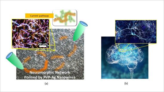
Caption: (a) Micrograph of the neuromorphic network fabricated by this research team. The network contains of numerous junctions between nanowires, which operate as synaptic elements. When voltage is applied to the network (between the green probes), current pathways (orange) are formed in the network. (b) A Human brain and one of its neuronal networks. The brain is known to have a complex network structure and to operate by means of electrical signal propagation across the network. Credit: NIMS
An international joint research team led by NIMS succeeded in fabricating a neuromorphic network composed of numerous metallic nanowires. Using this network, the team was able to generate electrical characteristics similar to those associated with higher order brain functions unique to humans, such as memorization, learning, forgetting, becoming alert and returning to calm. The team then clarified the mechanisms that induced these electrical characteristics.
The development of artificial intelligence (AI) techniques has been rapidly advancing in recent years and has begun impacting our lives in various ways. Although AI processes information in a manner similar to the human brain, the mechanisms by which human brains operate are still largely unknown. Fundamental brain components, such as neurons and the junctions between them (synapses), have been studied in detail. However, many questions concerning the brain as a collective whole need to be answered. For example, we still do not fully understand how the brain performs such functions as memorization, learning and forgetting, and how the brain becomes alert and returns to calm. In addition, live brains are difficult to manipulate in experimental research. For these reasons, the brain remains a “mysterious organ.” A different approach to brain research?in which materials and systems capable of performing brain-like functions are created and their mechanisms are investigated?may be effective in identifying new applications of brain-like information processing and advancing brain science.
The joint research team recently built a complex brain-like network by integrating numerous silver (Ag) nanowires coated with a polymer (PVP) insulating layer approximately 1 nanometer in thickness. A junction between two nanowires forms a variable resistive element (i.e., a synaptic element) that behaves like a neuronal synapse. This nanowire network, which contains a large number of intricately interacting synaptic elements, forms a “neuromorphic network”. When a voltage was applied to the neuromorphic network, it appeared to “struggle” to find optimal current pathways (i.e., the most electrically efficient pathways). The research team measured the processes of current pathway formation, retention and deactivation while electric current was flowing through the network and found that these processes always fluctuate as they progress, similar to the human brain’s memorization, learning, and forgetting processes. The observed temporal fluctuations also resemble the processes by which the brain becomes alert or returns to calm. Brain-like functions simulated by the neuromorphic network were found to occur as the huge number of synaptic elements in the network collectively work to optimize current transport, in the other words, as a result of self-organized and emerging dynamic processes..
The research team is currently developing a brain-like memory device using the neuromorphic network material. The team intends to design the memory device to operate using fundamentally different principles than those used in current computers. For example, while computers are currently designed to spend as much time and electricity as necessary in pursuit of absolutely optimum solutions, the new memory device is intended to make a quick decision within particular limits even though the solution generated may not be absolutely optimum. The team also hopes that this research will facilitate understanding of the brain’s information processing mechanisms.
This project was carried out by an international joint research team led by Tomonobu Nakayama (Deputy Director, International Center for Materials Nanoarchitectonics (WPI-MANA), NIMS), Adrian Diaz Alvarez (Postdoctoral Researcher, WPI-MANA, NIMS), Zdenka Kuncic (Professor, School of Physics, University of Sydney, Australia) and James K. Gimzewski (Professor, California NanoSystems Institute, University of California Los Angeles, USA).
Here at last is a link to and a citation for the paper,
Emergent dynamics of neuromorphic nanowire networks by Adrian Diaz-Alvarez, Rintaro Higuchi, Paula Sanz-Leon, Ido Marcus, Yoshitaka Shingaya, Adam Z. Stieg, James K. Gimzewski, Zdenka Kuncic & Tomonobu Nakayama. Scientific Reports volume 9, Article number: 14920 (2019) DOI: https://doi.org/10.1038/s41598-019-51330-6 Published: 17 October 2019
A close-up view of a new neuromorphic “brain-on-a-chip” that includes tens of thousands of memristors, or memory transistors. Credit: Peng Lin Courtesy: MIT
It’s hard to believe that a brain-on-a-chip might need sleep but that seems to be the case as far as the US Dept. of Energy’s Los Alamos National Laboratory is concerned. Before pursuing that line of thought, here’s some work from the Massachusetts Institute of Technology (MIT) involving memristors and a brain-on-a-chip. From a June 8, 2020 news item on ScienceDaily,
MIT engineers have designed a “brain-on-a-chip,” smaller than a piece of confetti, that is made from tens of thousands of artificial brain synapses known as memristors — silicon-based components that mimic the information-transmitting synapses in the human brain.
The researchers borrowed from principles of metallurgy to fabricate each memristor from alloys of silver and copper, along with silicon. When they ran the chip through several visual tasks, the chip was able to “remember” stored images and reproduce them many times over, in versions that were crisper and cleaner compared with existing memristor designs made with unalloyed elements.
Their results, published today in the journal Nature Nanotechnology, demonstrate a promising new memristor design for neuromorphic devices — electronics that are based on a new type of circuit that processes information in a way that mimics the brain’s neural architecture. Such brain-inspired circuits could be built into small, portable devices, and would carry out complex computational tasks that only today’s supercomputers can handle.
…
This ‘metallurgical’ approach differs somewhat from the protein nanowire approach used by the University of Massachusetts at Amherst team mentioned in my June 15, 2020 posting. Scientists are pursuing multiple pathways and we may find that we arrive with not ‘a single artificial brain but with many types of artificial brains.
“So far, artificial synapse networks exist as software. We’re trying to build real neural network hardware for portable artificial intelligence systems,” says Jeehwan Kim, associate professor of mechanical engineering at MIT. “Imagine connecting a neuromorphic device to a camera on your car, and having it recognize lights and objects and make a decision immediately, without having to connect to the internet. We hope to use energy-efficient memristors to do those tasks on-site, in real-time.”
Wandering ions
Memristors, or memory transistors [Note: Memristors are usually described as memory resistors; this is the first time I’ve seen ‘memory transistor’], are an essential element in neuromorphic computing. In a neuromorphic device, a memristor would serve as the transistor in a circuit, though its workings would more closely resemble a brain synapse — the junction between two neurons. The synapse receives signals from one neuron, in the form of ions, and sends a corresponding signal to the next neuron.
A transistor in a conventional circuit transmits information by switching between one of only two values, 0 and 1, and doing so only when the signal it receives, in the form of an electric current, is of a particular strength. In contrast, a memristor would work along a gradient, much like a synapse in the brain. The signal it produces would vary depending on the strength of the signal that it receives. This would enable a single memristor to have many values, and therefore carry out a far wider range of operations than binary transistors.
Like a brain synapse, a memristor would also be able to “remember” the value associated with a given current strength, and produce the exact same signal the next time it receives a similar current. This could ensure that the answer to a complex equation, or the visual classification of an object, is reliable — a feat that normally involves multiple transistors and capacitors.
Ultimately, scientists envision that memristors would require far less chip real estate than conventional transistors, enabling powerful, portable computing devices that do not rely on supercomputers, or even connections to the Internet.
Existing memristor designs, however, are limited in their performance. A single memristor is made of a positive and negative electrode, separated by a “switching medium,” or space between the electrodes. When a voltage is applied to one electrode, ions from that electrode flow through the medium, forming a “conduction channel” to the other electrode. The received ions make up the electrical signal that the memristor transmits through the circuit. The size of the ion channel (and the signal that the memristor ultimately produces) should be proportional to the strength of the stimulating voltage.
Kim says that existing memristor designs work pretty well in cases where voltage stimulates a large conduction channel, or a heavy flow of ions from one electrode to the other. But these designs are less reliable when memristors need to generate subtler signals, via thinner conduction channels.
The thinner a conduction channel, and the lighter the flow of ions from one electrode to the other, the harder it is for individual ions to stay together. Instead, they tend to wander from the group, disbanding within the medium. As a result, it’s difficult for the receiving electrode to reliably capture the same number of ions, and therefore transmit the same signal, when stimulated with a certain low range of current.
Borrowing from metallurgy
Kim and his colleagues found a way around this limitation by borrowing a technique from metallurgy, the science of melding metals into alloys and studying their combined properties.
“Traditionally, metallurgists try to add different atoms into a bulk matrix to strengthen materials, and we thought, why not tweak the atomic interactions in our memristor, and add some alloying element to control the movement of ions in our medium,” Kim says.
Engineers typically use silver as the material for a memristor’s positive electrode. Kim’s team looked through the literature to find an element that they could combine with silver to effectively hold silver ions together, while allowing them to flow quickly through to the other electrode.
The team landed on copper as the ideal alloying element, as it is able to bind both with silver, and with silicon.
“It acts as a sort of bridge, and stabilizes the silver-silicon interface,” Kim says.
To make memristors using their new alloy, the group first fabricated a negative electrode out of silicon, then made a positive electrode by depositing a slight amount of copper, followed by a layer of silver. They sandwiched the two electrodes around an amorphous silicon medium. In this way, they patterned a millimeter-square silicon chip with tens of thousands of memristors.
As a first test of the chip, they recreated a gray-scale image of the Captain America shield. They equated each pixel in the image to a corresponding memristor in the chip. They then modulated the conductance of each memristor that was relative in strength to the color in the corresponding pixel.
The chip produced the same crisp image of the shield, and was able to “remember” the image and reproduce it many times, compared with chips made of other materials.
The team also ran the chip through an image processing task, programming the memristors to alter an image, in this case of MIT’s Killian Court, in several specific ways, including sharpening and blurring the original image. Again, their design produced the reprogrammed images more reliably than existing memristor designs.
“We’re using artificial synapses to do real inference tests,” Kim says. “We would like to develop this technology further to have larger-scale arrays to do image recognition tasks. And some day, you might be able to carry around artificial brains to do these kinds of tasks, without connecting to supercomputers, the internet, or the cloud.”
Here’s a link to and a citation for the paper,
Alloying conducting channels for reliable neuromorphic computing by Hanwool Yeon, Peng Lin, Chanyeol Choi, Scott H. Tan, Yongmo Park, Doyoon Lee, Jaeyong Lee, Feng Xu, Bin Gao, Huaqiang Wu, He Qian, Yifan Nie, Seyoung Kim & Jeehwan Kim. Nature Nanotechnology (2020 DOI: https://doi.org/10.1038/s41565-020-0694-5 Published: 08 June 2020
This paper is behind a paywall.
Electric sheep and sleeping androids
I find it impossible to mention that androids might need sleep without reference to Philip K. Dick’s 1968 novel, “Do Androids Dream of Electric Sheep?”; its Wikipedia entry is here.
June 8, 2020
Intelligent machines of the future may need to sleep as much as we do.
Intelligent machines of the future may need to sleep as much as we do. Courtesy: Los Alamos National Laboratory
As it happens, I’m not the only one who felt the need to reference the novel, from a June 8, 2020 news item on ScienceDaily,
No one can say whether androids will dream of electric sheep, but they will almost certainly need periods of rest that offer benefits similar to those that sleep provides to living brains, according to new research from Los Alamos National Laboratory.
“We study spiking neural networks, which are systems that learn much as living brains do,” said Los Alamos National Laboratory computer scientist Yijing Watkins. “We were fascinated by the prospect of training a neuromorphic processor in a manner analogous to how humans and other biological systems learn from their environment during childhood development.”
Watkins and her research team found that the network simulations became unstable after continuous periods of unsupervised learning. When they exposed the networks to states that are analogous to the waves that living brains experience during sleep, stability was restored. “It was as though we were giving the neural networks the equivalent of a good night’s rest,” said Watkins.
The discovery came about as the research team worked to develop neural networks that closely approximate how humans and other biological systems learn to see. The group initially struggled with stabilizing simulated neural networks undergoing unsupervised dictionary training, which involves classifying objects without having prior examples to compare them to.
“The issue of how to keep learning systems from becoming unstable really only arises when attempting to utilize biologically realistic, spiking neuromorphic processors or when trying to understand biology itself,” said Los Alamos computer scientist and study coauthor Garrett Kenyon. “The vast majority of machine learning, deep learning, and AI researchers never encounter this issue because in the very artificial systems they study they have the luxury of performing global mathematical operations that have the effect of regulating the overall dynamical gain of the system.”
The researchers characterize the decision to expose the networks to an artificial analog of sleep as nearly a last ditch effort to stabilize them. They experimented with various types of noise, roughly comparable to the static you might encounter between stations while tuning a radio. The best results came when they used waves of so-called Gaussian noise, which includes a wide range of frequencies and amplitudes. They hypothesize that the noise mimics the input received by biological neurons during slow-wave sleep. The results suggest that slow-wave sleep may act, in part, to ensure that cortical neurons maintain their stability and do not hallucinate.
The groups’ next goal is to implement their algorithm on Intel’s Loihi neuromorphic chip. They hope allowing Loihi to sleep from time to time will enable it to stably process information from a silicon retina camera in real time. If the findings confirm the need for sleep in artificial brains, we can probably expect the same to be true of androids and other intelligent machines that may come about in the future.
Watkins will be presenting the research at the Women in Computer Vision Workshop on June 14 [2020] in Seattle.
The 2020 Women in Computer Vition Workshop (WICV) website is here. As is becoming standard practice for these times, the workshop was held in a virtual environment. Here’s a link to and a citation for the poster presentation paper,
Adding to the body of ‘memristor’ research I have here, there’s an April 17, 2019 news item on Nanowerk announcing the development of ‘memristor’ hardware by Japanese researchers (Note: A link has been removed),
A research group from Tohoku University has developed spintronics devices which are promising for future energy-efficient and adoptive computing systems, as they behave like neurons and synapses in the human brain (Advanced Materials, “Artificial Neuron and Synapse Realized in an Antiferromagnet/Ferromagnet Heterostructure Using Dynamics of Spin–Orbit Torque Switching”).
Today’s information society is built on digital computers that have evolved drastically for half a century and are capable of executing complicated tasks reliably. The human brain, by contrast, operates under very limited power and is capable of executing complex tasks efficiently using an architecture that is vastly different from that of digital computers.
So the development of computing schemes or hardware inspired by the processing of information in the brain is of broad interest to scientists in fields ranging from physics, chemistry, material science and mathematics, to electronics and computer science.
In computing, there are various ways to implement the processing of information by a brain. Spiking neural network is a kind of implementation method which closely mimics the brain’s architecture and temporal information processing. Successful implementation of spiking neural network requires dedicated hardware with artificial neurons and synapses that are designed to exhibit the dynamics of biological neurons and synapses.
Here, the artificial neuron and synapse would ideally be made of the same material system and operated under the same working principle. However, this has been a challenging issue due to the fundamentally different nature of the neuron and synapse in biological neural networks.
The research group – which includes Professor Hideo Ohno (currently the university president), Associate Professor Shunsuke Fukami, Dr. Aleksandr Kurenkov and Professor Yoshihiko Horio – created an artificial neuron and synapse by using spintronics technology. Spintronics is an academic field that aims to simultaneously use an electron’s electric (charge) and magnetic (spin) properties.
The research group had previously developed a functional material system consisting of antiferromagnetic and ferromagnetic materials. This time, they prepared artificial neuronal and synaptic devices microfabricated from the material system, which demonstrated fundamental behavior of biological neuron and synapse – leaky integrate-and-fire and spike-timing-dependent plasticity, respectively – based on the same concept of spintronics.
The spiking neural network is known to be advantageous over today’s artificial intelligence for the processing and prediction of temporal information. Expansion of the developed technology to unit-circuit, block and system levels is expected to lead to computers that can process time-varying information such as voice and video with a small amount of power or edge devices that have the an ability to adopt users and the environment through usage.
Simone Fabiano and Jennifer Gerasimov have developed a learning transistor that mimics the way synapses function. Credit: Thor Balkhed
At a guess, this was originally a photograph which has been passed through some sort of programme to give it a paintinglike quality.
Moving onto the research, I don’t see any reference to memristors (another of the ‘devices’ that mimics the human brain) so perhaps this is an entirely different way to mimic human brains? A February 5, 2019 news item on ScienceDaily announces the work from Linkoping University (Sweden),
A new transistor based on organic materials has been developed by scientists at Linköping University. It has the ability to learn, and is equipped with both short-term and long-term memory. The work is a major step on the way to creating technology that mimics the human brain.
Until now, brains have been unique in being able to create connections where there were none before. In a scientific article in Advanced Science, researchers from Linköping University describe a transistor that can create a new connection between an input and an output. They have incorporated the transistor into an electronic circuit that learns how to link a certain stimulus with an output signal, in the same way that a dog learns that the sound of a food bowl being prepared means that dinner is on the way.
A normal transistor acts as a valve that amplifies or dampens the output signal, depending on the characteristics of the input signal. In the organic electrochemical transistor that the researchers have developed, the channel in the transistor consists of an electropolymerised conducting polymer. The channel can be formed, grown or shrunk, or completely eliminated during operation. It can also be trained to react to a certain stimulus, a certain input signal, such that the transistor channel becomes more conductive and the output signal larger.
“It is the first time that real time formation of new electronic components is shown in neuromorphic devices”, says Simone Fabiano, principal investigator in organic nanoelectronics at the Laboratory of Organic Electronics, Campus Norrköping.
The channel is grown by increasing the degree of polymerisation of the material in the transistor channel, thereby increasing the number of polymer chains that conduct the signal. Alternatively, the material may be overoxidised (by applying a high voltage) and the channel becomes inactive. Temporary changes of the conductivity can also be achieved by doping or dedoping the material.
“We have shown that we can induce both short-term and permanent changes to how the transistor processes information, which is vital if one wants to mimic the ways that brain cells communicate with each other”, says Jennifer Gerasimov, postdoc in organic nanoelectronics and one of the authors of the article.
By changing the input signal, the strength of the transistor response can be modulated across a wide range, and connections can be created where none previously existed. This gives the transistor a behaviour that is comparable with that of the synapse, or the communication interface between two brain cells.
It is also a major step towards machine learning using organic electronics. Software-based artificial neural networks are currently used in machine learning to achieve what is known as “deep learning”. Software requires that the signals are transmitted between a huge number of nodes to simulate a single synapse, which takes considerable computing power and thus consumes considerable energy.
“We have developed hardware that does the same thing, using a single electronic component”, says Jennifer Gerasimov.
“Our organic electrochemical transistor can therefore carry out the work of thousands of normal transistors with an energy consumption that approaches the energy consumed when a human brain transmits signals between two cells”, confirms Simone Fabiano.
The transistor channel has not been constructed using the most common polymer used in organic electronics, PEDOT, but instead using a polymer of a newly-developed monomer, ETE-S, produced by Roger Gabrielsson, who also works at the Laboratory of Organic Electronics and is one of the authors of the article. ETE-S has several unique properties that make it perfectly suited for this application – it forms sufficiently long polymer chains, is water-soluble while the polymer form is not, and it produces polymers with an intermediate level of doping. The polymer PETE-S is produced in its doped form with an intrinsic negative charge to balance the positive charge carriers (it is p-doped).
There’s one other image associated this work that I want to include here,
Synaptic transistor. Sketch of the organic electrochemical transistor, formed by electropolymerization of ETE‐S in the transistor channel. The electrolyte solution is confined by a PDMS well (not shown). In this work, we define the input at the gate as the presynaptic signal and the response at the drain as the postsynaptic terminal. During operation, the drain voltage is kept constant while the gate is pulsed. Synaptic weight is defined as the amplitude of the current response to a standard gate voltage characterization pulse of −0.1 V. Different memory functionalities are accessible by applying gate voltage Courtesy: Linkoping University Researchers
Down the memristor rabbit hole one more time.* I started out with news about two new papers and inadvertently found two more. In a bid to keep this posting to a manageable size, I’m stopping at four.
Memristor (or memory resistors) devices are non-volatile electronic memory devices that were first theorized by Leon Chua in the 1970’s. However, it was some thirty years later that the first practical device was fabricated. This was in 2008 when a group led by Stanley Williams at HP Research Labs realized that switching of the resistance between a conducting and less conducting state in metal-oxide thin-film devices was showing Leon Chua’s memristor behaviour.
…
The high interest in memristor devices also stems from the fact that these devices emulate the memory and learning properties of biological synapses. i.e. the electrical resistance value of the device is dependent on the history of the current flowing through it.
There is a huge effort underway to use memristor devices in neuromorphic computing applications and it is now reasonable to imagine the development of a new generation of artificial intelligent devices with very low power consumption (non-volatile), ultra-fast performance and high-density integration.
These discoveries come at an important juncture in microelectronics, since there is increasing disparity between computational needs of Big Data, Artificial Intelligence (A.I.) and the Internet of Things (IoT), and the capabilities of existing computers. The increases in speed, efficiency and performance of computer technology cannot continue in the same manner as it has done since the 1960s.
…
To date, most memristor research has focussed on the electronic switching properties of the device. However, for many applications it is useful to have an additional handle (or degree of freedom) on the device to control its resistive state. For example memory and processing in the brain also involves numerous chemical and bio-chemical reactions that control the brain structure and its evolution through development.
To emulate this in a simple solid-state system composed of just switches alone is not possible. In our research, we are interested in using light to mediate this essential control.
…
We have demonstrated that light can be used to make short and long-term memory and we have shown how light can modulate a special type of learning, called spike timing dependent plasticity (STDP). STDP involves two neuronal spikes incident across a synapse at the same time. Depending on the relative timing of the spikes and their overlap across the synaptic cleft, the connection strength is other strengthened or weakened.
In our earlier work, we were only able to achieve to small switching effects in memristors using light. In our latest work (Advanced Electronic Materials, “Percolation Threshold Enables Optical Resistive-Memory Switching and Light-Tuneable Synaptic Learning in Segregated Nanocomposites”), we take advantage of a percolating-like nanoparticle morphology to vastly increase the magnitude of the switching between electronic resistance states when light is incident on the device.
…
We have used an inhomogeneous percolating network consisting of metallic nanoparticles distributed in filamentary-like conduction paths. Electronic conduction and the resistance of the device is very sensitive to any disruption of the conduction path(s).
By embedding the nanoparticles in a polymer that can expand or contract with light the conduction pathways are broken or re-connected causing very large changes in the electrical resistance and memristance of the device.
Our devices could lead to the development of new memristor-based artificial intelligence systems that are adaptive and reconfigurable using a combination of optical and electronic signalling. Furthermore, they have the potential for the development of very fast optical cameras for artificial intelligence recognition systems.
Our work provides a nice proof-of-concept but the materials used means the optical switching is slow. The materials are also not well suited to industry fabrication. In our on-going work we are addressing these switching speed issues whilst also focussing on industry compatible materials.
Currently we are working on a new type of optical memristor device that should give us orders of magnitude improvement in the optical switching speeds whilst also retaining a large difference between the resistance on and off states. We hope to be able to achieve nanosecond switching speeds. The materials used are also compatible with industry standard methods of fabrication.
The new devices should also have applications in optical communications, interfacing and photonic computing. We are currently looking for commercial investors to help fund the research on these devices so that we can bring the device specifications to a level of commercial interest.
…
If you’re interested in memristors, Kemp’s article is well written and quite informative for nonexperts, assuming of course you can tolerate not understanding everything perfectly.
Here are links and citations for two papers. The first is the latest referred to in the article, a May 2019 paper and the second is a paper appearing in July 2019.
Memristors, demonstrated by solid-state devices with continuously tunable resistance, have emerged as a new paradigm for self-adaptive networks that require synapse-like functions. Spin-based memristors offer advantages over other types of memristors because of their significant endurance and high energy effciency.
However, it remains a challenge to build dense and functional spintronic memristors with structures and materials that are compatible with existing ferromagnetic devices. Ta/CoFeB/MgO heterostructures are commonly used in interfacial PMA-based [perpendicular magnetic anisotropy] magnetic tunnel junctions, which exhibit large tunnel magnetoresistance and are implemented in commercial MRAM [magnetic random access memory] products.
“To achieve the memristive function, DW is driven back and forth in a continuous manner in the CoFeB layer by applying in-plane positive or negative current pulses along the Ta layer, utilizing SOT that the current exerts on the CoFeB magnetization,” said Shuai Zhang, a coauthor in the paper. “Slowly propagating domain wall generates a creep in the detection area of the device, which yields a broad range of intermediate resistive states in the AHE [anomalous Hall effect] measurements. Consequently, AHE resistance is modulated in an analog manner, being controlled by the pulsed current characteristics including amplitude, duration, and repetition number.”
“For a follow-up study, we are working on more neuromorphic operations, such as spike-timing-dependent plasticity and paired pulsed facilitation,” concludes You. …
Here’s are links to and citations for the paper (Note: It’s a little confusing but I believe that one of the links will take you to the online version, as for the ‘open access’ link, keep reading),
A Spin–Orbit‐Torque Memristive Device by Shuai Zhang, Shijiang Luo, Nuo Xu, Qiming Zou, Min Song, Jijun Yun, Qiang Luo, Zhe Guo, Ruofan Li, Weicheng Tian, Xin Li, Hengan Zhou, Huiming Chen, Yue Zhang, Xiaofei Yang, Wanjun Jiang, Ka Shen, Jeongmin Hong, Zhe Yuan, Li Xi, Ke Xia, Sayeef Salahuddin, Bernard Dieny, Long You. Advanced Electronic Materials Volume 5, Issue 4 April 2019 (print version) 1800782 DOI: https://doi.org/10.1002/aelm.201800782 First published [online]: 30 January 2019 Note: there is another DOI, https://doi.org/10.1002/aelm.201970022 where you can have open access to Memristors: A Spin–Orbit‐Torque Memristive Device (Adv. Electron. Mater. 4/2019)
The paper published online in January 2019 is behind a paywall and the paper (almost the same title) published in April 2019 has a new DOI and is open access. Final note: I tried accessing the ‘free’ paper and opened up a free file for the artwork featuring the work from China on the back cover of the April 2019 of Advanced Electronic Materials.
Korea
Usually when I see the words transparency and flexibility, I expect to see graphene is one of the materials. That’s not the case for this paper (link to and citation for),
Here’s the abstract for the paper where you’ll see that the material is made up of zinc oxide silver nanowires,
An artificial photonic synapse having tunable manifold synaptic response can be an essential step forward for the advancement of novel neuromorphic computing. In this work, we reported the development of highly transparent and flexible two-terminal ZnO/Ag-nanowires/PET photonic artificial synapse [emphasis mine]. The device shows purely photo-triggered all essential synaptic functions such as transition from short-to long-term plasticity, paired-pulse facilitation, and spike-timing-dependent plasticity, including in the versatile memory capability. Importantly, strain-induced piezo-phototronic effect within ZnO provides an additional degree of regulation to modulate all of the synaptic functions in multi-levels. The observed effect is quantitatively explained as a dynamic of photo-induced electron-hole trapping/detraining via the defect states such as oxygen vacancies. We revealed that the synaptic functions can be consolidated and converted by applied strain, which is not previously applied any of the reported synaptic devices. This study will open a new avenue to the scientific community to control and design highly transparent wearable neuromorphic computing.
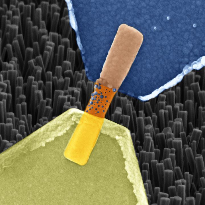
Caption: Image captured by an electron microscope of a single nanowire memristor (highlighted in colour to distinguish it from other nanowires in the background image). Blue: silver electrode, orange: nanowire, yellow: platinum electrode. Blue bubbles are dispersed over the nanowire. They are made up of silver ions and form a bridge between the electrodes which increases the resistance. Credit: Forschungszentrum Jülich
Not a popsicle but a representation of a device (memristor) scientists claim mimics a biological nerve cell according to a December 5, 2018 news item on ScienceDaily,
Scientists from Jülich [Germany] together with colleagues from Aachen [Germany] and Turin [Italy] have produced a memristive element made from nanowires that functions in much the same way as a biological nerve cell. The component is able to both save and process information, as well as receive numerous signals in parallel. The resistive switching cell made from oxide crystal nanowires is thus proving to be the ideal candidate for use in building bioinspired “neuromorphic” processors, able to take over the diverse functions of biological synapses and neurons.
Computers have learned a lot in recent years. Thanks to rapid progress in artificial intelligence they are now able to drive cars, translate texts, defeat world champions at chess, and much more besides. In doing so, one of the greatest challenges lies in the attempt to artificially reproduce the signal processing in the human brain. In neural networks, data are stored and processed to a high degree in parallel. Traditional computers on the other hand rapidly work through tasks in succession and clearly distinguish between the storing and processing of information. As a rule, neural networks can only be simulated in a very cumbersome and inefficient way using conventional hardware.
Systems with neuromorphic chips that imitate the way the human brain works offer significant advantages. Experts in the field describe this type of bioinspired computer as being able to work in a decentralised way, having at its disposal a multitude of processors, which, like neurons in the brain, are connected to each other by networks. If a processor breaks down, another can take over its function. What is more, just like in the brain, where practice leads to improved signal transfer, a bioinspired processor should have the capacity to learn.
“With today’s semiconductor technology, these functions are to some extent already achievable. These systems are however suitable for particular applications and require a lot of space and energy,” says Dr. Ilia Valov from Forschungszentrum Jülich. “Our nanowire devices made from zinc oxide crystals can inherently process and even store information, as well as being extremely small and energy efficient,” explains the researcher from Jülich’s Peter Grünberg Institute.
For years memristive cells have been ascribed the best chances of being capable of taking over the function of neurons and synapses in bioinspired computers. They alter their electrical resistance depending on the intensity and direction of the electric current flowing through them. In contrast to conventional transistors, their last resistance value remains intact even when the electric current is switched off. Memristors are thus fundamentally capable of learning.
In order to create these properties, scientists at Forschungszentrum Jülich and RWTH Aachen University used a single zinc oxide nanowire, produced by their colleagues from the polytechnic university in Turin. Measuring approximately one ten-thousandth of a millimeter in size, this type of nanowire is over a thousand times thinner than a human hair. The resulting memristive component not only takes up a tiny amount of space, but also is able to switch much faster than flash memory.
Nanowires offer promising novel physical properties compared to other solids and are used among other things in the development of new types of solar cells, sensors, batteries and computer chips. Their manufacture is comparatively simple. Nanowires result from the evaporation deposition of specified materials onto a suitable substrate, where they practically grow of their own accord.
In order to create a functioning cell, both ends of the nanowire must be attached to suitable metals, in this case platinum and silver. The metals function as electrodes, and in addition, release ions triggered by an appropriate electric current. The metal ions are able to spread over the surface of the wire and build a bridge to alter its conductivity.
Components made from single nanowires are, however, still too isolated to be of practical use in chips. Consequently, the next step being planned by the Jülich and Turin researchers is to produce and study a memristive element, composed of a larger, relatively easy to generate group of several hundred nanowires offering more exciting functionalities.
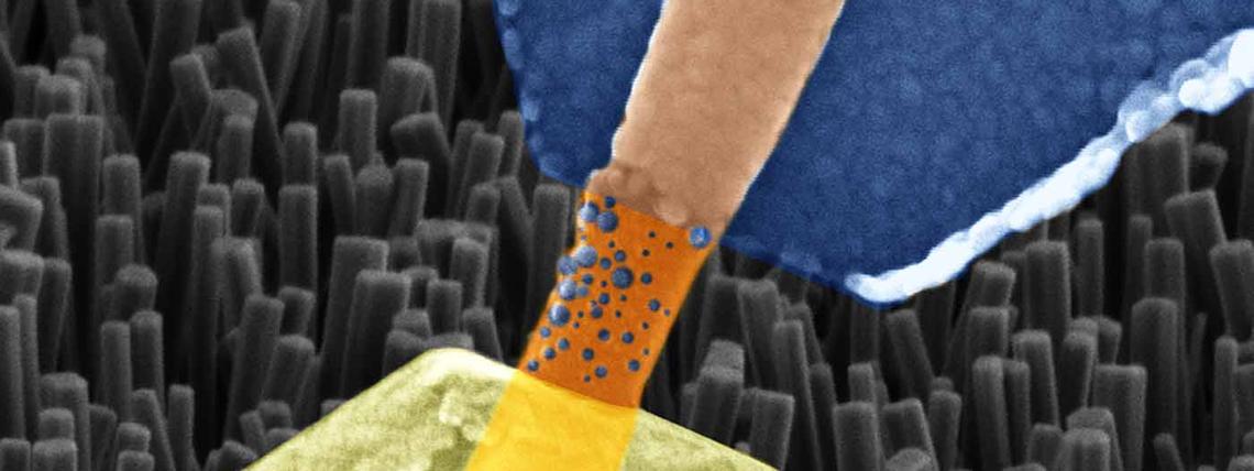
The Italians have also written about the work in a December 4, 2018 news item for the Polytecnico di Torino’s inhouse magazine, PoliFlash’. I like the image they’ve used better as it offers a bit more detail and looks less like a popsicle. First, the image,
Courtesy: Polytecnico di Torino
Now, the news item, which includes some historical information about the memristor (Note: There is some repetition and links have been removed),
Emulating and understanding the human brain is one of the most important challenges for modern technology: on the one hand, the ability to artificially reproduce the processing of brain signals is one of the cornerstones for the development of artificial intelligence, while on the other the understanding of the cognitive processes at the base of the human mind is still far away.
And the research published in the prestigious journal Nature Communications by Gianluca Milano and Carlo Ricciardi, PhD student and professor, respectively, of the Applied Science and Technology Department of the Politecnico di Torino, represents a step forward in these directions. In fact, the study entitled “Self-limited single nanowire systems combining all-in-one memristive and neuromorphic functionalities” shows how it is possible to artificially emulate the activity of synapses, i.e. the connections between neurons that regulate the learning processes in our brain, in a single “nanowire” with a diameter thousands of times smaller than that of a hair.
It is a crystalline nanowire that takes the “memristor”, the electronic device able to artificially reproduce the functions of biological synapses, to a more performing level. Thanks to the use of nanotechnologies, which allow the manipulation of matter at the atomic level, it was for the first time possible to combine into one single device the synaptic functions that were individually emulated through specific devices. For this reason, the nanowire allows an extreme miniaturisation of the “memristor”, significantly reducing the complexity and energy consumption of the electronic circuits necessary for the implementation of learning algorithms.
Starting from the theorisation of the “memristor” in 1971 by Prof. Leon Chua – now visiting professor at the Politecnico di Torino, who was conferred an honorary degree by the University in 2015 – this new technology will not only allow smaller and more performing devices to be created for the implementation of increasingly “intelligent” computers, but is also a significant step forward for the emulation and understanding of the functioning of the brain.
“The nanowire memristor – said Carlo Ricciardi – represents a model system for the study of physical and electrochemical phenomena that govern biological synapses at the nanoscale. The work is the result of the collaboration between our research team and the RWTH University of Aachen in Germany, supported by INRiM, the National Institute of Metrological Research, and IIT, the Italian Institute of Technology.”
It seems the US National Institute of Standards and Technology (NIST) is more deeply invested into developing artificial brains than I had realized (See: April 17, 2018 posting). A January 26, 2018 NIST news release on EurekAlert describes the organization’s latest foray into the field,
Researchers at the National Institute of Standards and Technology (NIST) have built a superconducting switch that “learns” like a biological system and could connect processors and store memories in future computers operating like the human brain.
The NIST switch, described in Science Advances, is called a synapse, like its biological counterpart, and it supplies a missing piece for so-called neuromorphic computers. Envisioned as a new type of artificial intelligence, such computers could boost perception and decision-making for applications such as self-driving cars and cancer diagnosis.
A synapse is a connection or switch between two brain cells. NIST’s artificial synapse–a squat metallic cylinder 10 micrometers in diameter–is like the real thing because it can process incoming electrical spikes to customize spiking output signals. This processing is based on a flexible internal design that can be tuned by experience or its environment. The more firing between cells or processors, the stronger the connection. Both the real and artificial synapses can thus maintain old circuits and create new ones. Even better than the real thing, the NIST synapse can fire much faster than the human brain–1 billion times per second, compared to a brain cell’s 50 times per second–using just a whiff of energy, about one ten-thousandth as much as a human synapse. In technical terms, the spiking energy is less than 1 attojoule, lower than the background energy at room temperature and on a par with the chemical energy bonding two atoms in a molecule.
“The NIST synapse has lower energy needs than the human synapse, and we don’t know of any other artificial synapse that uses less energy,” NIST physicist Mike Schneider said.
The new synapse would be used in neuromorphic computers made of superconducting components, which can transmit electricity without resistance, and therefore, would be more efficient than other designs based on semiconductors or software. Data would be transmitted, processed and stored in units of magnetic flux. Superconducting devices mimicking brain cells and transmission lines have been developed, but until now, efficient synapses–a crucial piece–have been missing.
The brain is especially powerful for tasks like context recognition because it processes data both in sequence and simultaneously and stores memories in synapses all over the system. A conventional computer processes data only in sequence and stores memory in a separate unit.
The NIST synapse is a Josephson junction, long used in NIST voltage standards. These junctions are a sandwich of superconducting materials with an insulator as a filling. When an electrical current through the junction exceeds a level called the critical current, voltage spikes are produced. The synapse uses standard niobium electrodes but has a unique filling made of nanoscale clusters of manganese in a silicon matrix.
The nanoclusters–about 20,000 per square micrometer–act like tiny bar magnets with “spins” that can be oriented either randomly or in a coordinated manner.
“These are customized Josephson junctions,” Schneider said. “We can control the number of nanoclusters pointing in the same direction, which affects the superconducting properties of the junction.”
The synapse rests in a superconducting state, except when it’s activated by incoming current and starts producing voltage spikes. Researchers apply current pulses in a magnetic field to boost the magnetic ordering, that is, the number of nanoclusters pointing in the same direction. This magnetic effect progressively reduces the critical current level, making it easier to create a normal conductor and produce voltage spikes.
The critical current is the lowest when all the nanoclusters are aligned. The process is also reversible: Pulses are applied without a magnetic field to reduce the magnetic ordering and raise the critical current. This design, in which different inputs alter the spin alignment and resulting output signals, is similar to how the brain operates.
Synapse behavior can also be tuned by changing how the device is made and its operating temperature. By making the nanoclusters smaller, researchers can reduce the pulse energy needed to raise or lower the magnetic order of the device. Raising the operating temperature slightly from minus 271.15 degrees C (minus 456.07 degrees F) to minus 269.15 degrees C (minus 452.47 degrees F), for example, results in more and higher voltage spikes.
Crucially, the synapses can be stacked in three dimensions (3-D) to make large systems that could be used for computing. NIST researchers created a circuit model to simulate how such a system would operate.
The NIST synapse’s combination of small size, superfast spiking signals, low energy needs and 3-D stacking capability could provide the means for a far more complex neuromorphic system than has been demonstrated with other technologies, according to the paper.
NIST has prepared an animation illustrating the research,
Caption: This is an animation of how NIST’s artificial synapse works. Credit: Sean Kelley/NIST
Here’s a link to and a citation for the paper,
Ultralow power artificial synapses using nanotextured magnetic Josephson junctions by Michael L. Schneider, Christine A. Donnelly, Stephen E. Russek, Burm Baek, Matthew R. Pufall, Peter F. Hopkins, Paul D. Dresselhaus, Samuel P. Benz, and William H. Rippard. Science Advances 26 Jan 2018: Vol. 4, no. 1, e1701329 DOI: 10.1126/sciadv.1701329
This paper is open access.
Samuel K. Moore in a January 26, 2018 posting on the Nanoclast blog (on the IEEE [Institute for Electrical and Electronics Engineers] website) describes the research and adds a few technical explanations such as this about the Josephson junction,
In a magnetic Josephson junction, that “weak link” is magnetic. The higher the magnetic field, the lower the critical current needed to produce voltage spikes. In the device Schneider and his colleagues designed, the magnetic field is caused by 20,000 or so nanometer-scale clusters of manganese embedded in silicon. …
Moore also provides some additional links including this one to his November 29, 2017 posting where he describes four new approaches to computing including quantum computing and neuromorphic (brain-like) computing.