Tag Archives: A*STAR

Gold nanoparticles as catalysts for clear water and hydrogen production

The research was published online May 2014 and in a July 2014 print version,  which seems a long time ago now but there’s a renewed interest in attracting attention for this work. A Dec. 17, 2014 news item on phys.org describes this proposed water purification technology from Singapore’s A*STAR (Agency for Science Technology and Research), Note: Links have been removed,

A new catalyst could have dramatic environmental benefits if it can live up to its potential, suggests research from Singapore. A*STAR researchers have produced a catalyst with gold-nanoparticle antennas that can improve water quality in daylight and also generate hydrogen as a green energy source.

This water purification technology was developed by He-Kuan Luo, Andy Hor and colleagues from the A*STAR Institute of Materials Research and Engineering (IMRE). “Any innovative and benign technology that can remove or destroy organic pollutants from water under ambient conditions is highly welcome,” explains Hor, who is executive director of the IMRE and also affiliated with the National University of Singapore.

A Dec. 17, 2014 A*STAR research highlight, which originated the news item, describes the photocatalytic process the research team developed and tested,

Photocatalytic materials harness sunlight to create electrical charges, which provide the energy needed to drive chemical reactions in molecules attached to the catalyst’s surface. In addition to decomposing harmful molecules in water, photocatalysts are used to split water into its components of oxygen and hydrogen; hydrogen can then be employed as a green energy source.

Hor and his team set out to improve an existing catalyst. Oxygen-based compounds such as strontium titanate (SrTiO3) look promising, as they are robust and stable materials and are suitable for use in water. One of the team’s innovations was to enhance its catalytic activity by adding small quantities of the metal lanthanum, which provides additional usable electrical charges.

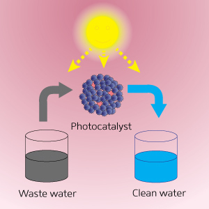
Catalysts also need to capture a sufficient amount of sunlight to catalyze chemical reactions. So to enable the photocatalyst to harvest more light, the scientists attached gold nanoparticles to the lanthanum-doped SrTiO3 microspheres (see image). These gold nanoparticles are enriched with electrons and hence act as antennas, concentrating light to accelerate the catalytic reaction.

The porous structure of the microspheres results in a large surface area, as it provides more binding space for organic molecules to dock to. A single gram of the material has a surface area of about 100 square meters. “The large surface area plays a critical role in achieving a good photocatalytic activity,” comments Luo.

To demonstrate the efficiency of these catalysts, the researchers studied how they decomposed the dye rhodamine B in water. Within four hours of exposure to visible light 92 per cent of the dye was gone, which is much faster than conventional catalysts that lack gold nanoparticles.

These microparticles can also be used for water splitting, says Luo. The team showed that the microparticles with gold nanoparticles performed better in water-splitting experiments than those without, further highlighting the versatility and effectiveness of these microspheres.

The researchers have provided an illustration of the process,

Improved photocatalyst microparticles containing gold nanoparticles can be used to purify water. © 2014 A*STAR Institute of Materials Research and Engineering

Improved photocatalyst microparticles containing gold nanoparticles can be used to purify water.
© 2014 A*STAR Institute of Materials Research and Engineering

Here’s a link to and a citation for the research paper,

Novel Au/La-SrTiO3 microspheres: Superimposed Effect of Gold Nanoparticles and Lanthanum Doping in Photocatalysis by Guannan Wang, Pei Wang, Dr. He-Kuan Luo, and Prof. T. S. Andy Hor. Chemistry – An Asian Journal Volume 9, Issue 7, pages 1854–1859, July 2014. Article first published online: 9 MAY 2014 DOI: 10.1002/asia.201402007

© 2014 WILEY-VCH Verlag GmbH & Co. KGaA, Weinheim

This article is behind a paywall.

Nanotechnology education, artificial muscles, and Estonian high schools?

The University of Tartu (Estonia) announced in a Sept. 29, 2014 press release an educational and entrepreneurial programme about nanotechnology/nanoscience for teachers and students,

Led by the University of Tartu, innovative Estonian schools participate in the Quantum Spin-Off project, which aims to bring youth in contact with nanotechnology, modern science and high-tech entrepreneurship. Pupils participating in the project will learn about seven topics of nanotechnology, including the creation of artificial muscles and the manipulation of nanoparticles.

Most people have little contact with nanoscience and nanotechnologies, although the exciting nano-world has always been around us. “Most Estonian teachers do not have the experience of introducing nanoscience required for understanding the nano-world or the necessary connections that would allow visiting the experts in nanoscience and enterprises using the technology,” said the leader of the Quantum Spin-Off project, UT Professor of Technology Education Margus Pedaste, describing the current situation of acquiring nanotechnology knowledge in Estonia.

Coordinator of the project, Project Manager at the Centre for Educational Technology Maarika Lukk adds that nanoscience is interesting and necessary, as it offers plenty of practical applications, for instance in medicine, education, military industry and space.

The press release goes on to describe the Quantum Spin-Off project and the proposed nanoscience programme in more detail,

To bring nanoscience closer to pupils, educational researchers of the University of Tartu decided to implement the European Union LLP Comenius project “Quantum Spin-Off – connecting schools with high-tech research and entrepreneurship”. The objective of the project is to build a kind of a bridge: at one end, pupils can familiarise themselves with modern science, and at the other, experience its application opportunities at high-tech enterprises. “We also wish to inspire these young people to choose a specialisation related to science and technology in the future,” added Lukk.

The pupils can choose between seven topics of nanotechnology: the creation of artificial muscles, microbiological fuel elements, manipulation of nanoparticles, nanoparticles and ionic liquids as oil additives, materials used in regenerative medicine, deposition and 3D-characterisation of atomically designed structures and a topic covered in English, “Artificial robotic fish with EAP elements”.

Learning is based on study modules in the field of nanotechnology. In addition, each team of pupils will read a scientific publication, selected for them by an expert of that particular field. In that way, pupils will develop an understanding of the field and of scientific texts. On the basis of the scientific publication, the pupils prepare their own research project and a business plan suitable for applying the results of the project.

In each field, experts of the University of Tartu will help to understand the topics. Participants will visit a nanotechnology research laboratory and enterprises using nanotechnologies.

The project lasts for two years and it is also implemented in Belgium, Switzerland and Greece.

You can find more information about the European Union’s Quantum Spin-Off Project on its website (from the homepage),

The Quantum Spinoff project will bring science teachers and their pupils in direct contact with research and entrepreneurship in the high-tech nano sector, with the goal of educating a new generation of scientifically literate European citizens and inspiring young people to choose for science and technology careers. Teams of pupils, guided by their science teachers, will be challenged to create a responsible and socially relevant valorisation of a scientific paper in collaboration with actual researchers and entrepreneurs. They will visit high-tech research labs and will compete for the European Quantum Spin-Off Prize. Scientific and technological insights, creativity and responsible entrepreneurship will be all taken into account by the jury of experts. Science teachers will be trained in international and national workshops to support the inquiry learning process of their pupils.

This drive toward linking science to entrepreneurial output is an international effort as this Quantum-Spin Off project , Singapore’s A*STAR (Agency for Science, Technology and Research) and my Sept. 30, 2014 post about the 2014 Canadian Science Policy Conference  make abundantly clear.

A rose by any other name: water pinning nanostructures and wettability

There are two items about rose petals as bioinspiration for research in this posting. The first being the most recent research where scientists in Singapore have made an ultrathin film modeled on rose petals. From an Aug. 13, 2014 news item on Nanowerk (Note: A link has been removed),

A*STAR [based in Singapore] researchers have used nanoimprinting methods to make patterned polymeric films with surface topography inspired by that of a rose petal, producing a range of transparent films with high water pinning forces (“Bioinspired Ultrahigh Water Pinning Nanostructures”).

An Aug. 13, 2014 A*STAR news highlight, which originated the news item, describes the nature of the research,

A surface to which a water droplet adheres, even when it is turned upside down, is described as having strong water pinning characteristics. A rose petal and a lotus leaf are both superhydrophobic, yet dissimilarities in their water pinning properties cause a water droplet to stick to a rose petal but roll off a lotus leaf. The two leaf types differ in their micro- and nanoscale surface topography and it is these topographical details that alter the water pinning force. The rose petal has almost uniformly distributed, conical-shaped microscale protrusions with nanoscale folds on these protrusions, while the lotus leaf has randomly distributed microscale protrusions.

The imprinted surfaces developed by Jaslyn Law and colleagues at the A*STAR Institute of Materials Research and Engineering and the Singapore University of Technology and Design have uniformly distributed patterns of nanoscale protrusions that are either conical or parabolic in shape. The researchers found that the water pinning forces on these continuously patterned surfaces were much greater than on non-patterned surfaces and surfaces composed of isolated nanopillared structures or nanoscale gratings. They could then achieve high water pinning forces by patterning the nanoprotrusions onto polymeric films with a range of different non-patterned hydrophobicities, including polycarbonate, poly(methyl methacrylate) and polydimethylsiloxane (see image).

“Other methods that recreate the water pinning effect have used actual rose petals as the mold, but unless special care is taken, there are likely to be defects and inconsistencies in the recreated pattern,” says co-author Andrew Ng. “While bottom-up approaches for making patterns — for example, laser ablation, liquid flame spray or chemical vapor deposition — are more consistent, these methods are limited in the types of patterns that can be used and the scale at which a substrate can be patterned.”

In contrast, nanoimprinting methods are capable of fabricating versatile and large-scale surfaces, and can be combined with roll-to-roll techniques, hence potentially enabling more commercial applications.

The patterned polycarbonate surfaces were also shown to reduce the ‘coffee-ring’ effect: the unevenly deposited film left behind upon the evaporation of a solute-laden droplet. This mitigation of the coffee-ring effect may assist microfluidic technologies and, more generally, the patterned surfaces could be used in arid regions for dew collection or in anti-drip applications such as in greenhouses.

The study which was published online in Dec. 2013, was featured in a Jan. 22, 2014 article by Katherine Bourzac for C&EN (Chemistry and Engineering News),

In the early morning, dew clings to rose petals; when the sun rises, the dewdrops act like tiny lenses, making diffraction patterns that attract pollinating insects, says Jaslyn Bee Khuan Law, a materials scientist at the Agency for Science, Technology, and Research (A*STAR), in Singapore. A drop of water will cling to a rose petal even when it’s tilted or held upside down. The petals can hold onto these droplets because their surfaces consist of closely packed conical structures a few micrometers across. These microscale surface patterns tweak the surface tension of the water droplets, causing them to cling to the petals.

But none of these fabrication methods are amenable to large-scale, low-cost manufacturing, preventing commercialization of the water-clinging surfaces. So Law turned to a specialty of her lab: nanoimprint lithography. This printing method utilizes metal or silicon drums molded with nanoscale features on their surfaces. When the molds are heated and pressed against sheets of plastic, the plastic is embossed with the nanoscale pattern. This roll-to-roll printing process resembles the way newspapers are printed. It’s capable of producing large-area films in a short amount of time.

Water droplets easily slid off plastic films patterned with simple nanoscale gratings; isolated nanoscale pillars hung onto water slightly better. But the films with the best properties consisted of tightly packed cones about 300 nm tall. Plastic patterned with these structures could hold onto water droplets as massive as 69 mg. The team could print a 110- by 65-mm sheet of this plastic film at a speed of 10 m per minute. Currently, the dimensions of the films are limited by the size of the premade molds, Law says.

While the Singapore group has made good progress on manufacturing these materials, very basic, vexing questions about how water clings to these surfaces remain, Hayes says. For example, very small changes in the surface’s roughness can switch it from water-pinning to super hydrophobic, and researchers don’t have a detailed understanding of why.

Here’s a link to and a citation for the paper,

Bioinspired Ultrahigh Water Pinning Nanostructures by Jaslyn Bee Khuan Law, Andrew Ming Hua Ng, Ai Yu He, and Hong Yee Low. Langmuir, 2014, 30 (1), pp 325–331 DOI: 10.1021/la4034996 Publication Date (Web): December 20, 2013
Copyright © 2013 American Chemical Society

This paper appears to be open access (I was able to access it by clicking on the HTML option).

Finally, here’s an image supplied by the A*Star researchers to illustrate their work,

[downloaded from http://pubs.acs.org/doi/full/10.1021/la4034996]

[downloaded from http://pubs.acs.org/doi/full/10.1021/la4034996]

This second rose petal item comes from Australia and dates from Fall 2013. From a Sept. 18, 2013 news item on ScienceDaily,

A new nanostructured material with applications that could include reducing condensation in airplane cabins and enabling certain medical tests without the need for high tech laboratories has been developed by researchers at the University of Sydney [Australia].

“The newly discovered material uses raspberry particles — so-called because of their appearance — which can trap tiny water droplets and prevent them from rolling off surfaces, even when that surface is turned upside down,” said Dr Andrew Telford from the University’s School of Chemistry and lead author of the research recently published in the journal, Chemistry of Materials.

The ability to immobilise [pin] very small droplets on a surface is, according to Dr Telford, a significant achievement with innumerable potential applications.

A Sept. 17, 2013 University of Sydney news release, which originated the news item, provides more insight into the research where the scientists have focused on ‘raspberry particles’ which could also be described as the ‘conical structures’ mentioned in the A*STAR work to achieve what appear to be similar ends,

Raspberry particles mimic the surface structure of some rose petals.

“Water droplets bead up in a spherical shape on top of rose petals,” Dr Telford said. “This is a sign the flower is highly water repellent.”

The reasons for this are complex and largely due to the special structure of the rose petal’s surface. The research team replicated the rose petal by assembling raspberry particles in the lab using spherical micro- and nanoparticles.

The result is that water droplets bead up when placed on films of the raspberry particles and they’re not able to drip down from it, even when turned upside down.

“Raspberry particle films can be described as sticky tape for water droplets,” Dr Telford said.

This could be useful in preventing condensation issues in airplane cabins. It could also help rapidly process simple medical tests on free-standing droplets, with the potential for very high turnover of tests with inexpensive equipment and in remote areas.

Other exciting applications are under study: if we use this nanotechnology to control how a surface is structured we can influence how it will interact with water.

“This means we will be able to design a surface that does whatever you need it to do.

“We could also design a surface that stays dry forever, never needs cleaning or able to repel bacteria or even prevent mould and fungi growth.

“We could then tweak the same structure by changing its composition so it forces water to spread very quickly.

“This could be used on quick-dry walls and roofs which would also help to cool down houses.

“This can only be achieved with a very clear understanding of the science behind the chemical properties and construction of the surface,” he said.

The discovery is also potentially viable commercially.

“Our team’s discovery is the first that allows for the preparation of raspberry particles on an industrial scale and we are now in a position where we can prepare large quantities of these particles without the need to build special plants or equipment,” Dr Telford said.

Here’s a link to and a citation for the Australian paper,

Mimicking the Wettability of the Rose Petal using Self-assembly of Waterborne Polymer Particles by A. M. Telford, B. S. Hawkett, C. Such, and C. Neto. Chem. Mater., 2013, 25 (17), pp 3472–3479 DOI: 10.1021/cm4016386 Publication Date (Web): July 23, 2013
Copyright © 2013 American Chemical Society

This paper is behind a paywall.
Fungal infections, begone!

A May 7, 2014 news item on Nanowerk highlights some antifungal research at A*STAR (Singapore’s Agency for Science, Technology and Research),

Pathogenic fungi like Candida albicans can cause oral, skin, nail and genital infections. While exposure to pathogenic fungi is generally not life-threatening, it can be deadly to immunocompromised patients with AIDS or cancer. A variety of antifungal medications, such as triazoles and polyenes, are currently used for treating fungal infections. The range of these antifungal medications, however, is extremely limited, with some fungal species developing resistance to these drugs.

Yi Yan Yang at the A*STAR Institute of Bioengineering and Nanotechnology in Singapore and co-workers, in collaboration with IBM Almaden Research Center in the United States, have discovered four cationic terephthalamide-bisurea compounds with strong antifungal activity, excellent microbial selectivity and low host toxicity …

A May 7, 2018 A*STAR news release, which originated the news item, describes the research in detail (Note: A link has been removed),

Conformational analysis revealed that the terephthalamide-bisurea compounds have a Z-shaped structure: the terephthalamide sits in the middle, urea groups on both sides of the terephthalamide, and cationic charges at both ends. The researchers prepared compounds with different spacers — ethyl, butyl, hexyl or benzyl amine — in-between the urea group and the cationic charge.

When dissolved in water, the terephthalamide-bisurea compounds aggregate to form fibers with lengths ranging from a few hundred nanometers to several micrometers. Some of the compounds form fibers with high flexibility and others with high rigidity.

The researchers evaluated the antifungal activity of their terephthalamide-bisurea compounds against C. albicans. They found that all of the cationic compounds effectively inhibited fungal growth, even when the fungal concentration increased from 102 to 105 colony-forming units per milliliter.

The researchers believe that the potent antifungal activity is largely due to the formation of fibers with extremely small diameters in the order of 5 to 10 nanometers, which facilitates the rupture of fungal membranes. “This is particularly important because the fungal membrane of C. albicans is multilayered and has low negative charges,” explains Yang. “It also helps explain why cationic terephthalamide-bisurea compounds could easily penetrate the fungal membrane.”

The terephthalamide-bisurea compounds also eradicated clinically isolated drug-resistant C. albicans. The compounds prevent the development of drug resistance by rupturing the fungal membrane of C. albicans and disrupting the biofilm (see image).

Additionally, cytotoxicity tests showed that the cationic terephthalamide-bisurea compounds exhibit low toxicity toward mammalian cells and in a mouse model, revealing that the compounds “are relatively safe for preventing and treating fungal infections,” says Yang. [emphasis mine]

It’s nice to see that this potential anti-fungal treatment isn’t damaging to one’s cells.

Here’s a link to and a citation for the paper,

Supramolecular high-aspect ratio assemblies with strong antifungal activity by Kazuki Fukushima, Shaoqiong Liu, Hong Wu, Amanda C. Engler, Daniel J. Coady, Hareem Maune, Jed Pitera, Alshakim Nelson, Nikken Wiradharma, Shrinivas Venkataraman, Yuan Huang, Weimin Fan, Jackie Y. Ying, Yi Yan Yang, & James L. Hedrick. Nature Communications 4, Article number: 286 doi:10.1038/ncomms3861 Published 09 December 2013

This article is behind a paywall.

Purple promises and bioimaging from Singapore’s A*STAR

A May 7, 2014 news item on Nanowerk describes a promising new approach to bioimaging,

Labeling biomolecules with light-emitting nanoparticles is a powerful technique for observing cell movement and signaling under realistic, in vivo conditions. The small size of these probes, however, often limits their optical capabilities. In particular, many nanoparticles have trouble producing high-energy light with wavelengths in the violet to ultraviolet range, which can trigger critical biological reactions.

Now, an international team led by Xiaogang Liu from the A*STAR Institute of Materials Research and Engineering and the National University of Singapore has discovered a novel class of rare-earth nanocrystals that preserve excited energy inside their atomic framework, resulting in unusually intense violet emissions …

A May 7, 2014 A*STAR (Agency for Science, Technology and Research) news release (h/t Imagist), which originated the news item, describes the problems with current bioimaging techniques and the new approach in more detail (Note: Links have been removed)

Nanocrystals selectively infused, or ‘doped’, with rare-earth ions have attracted the attention of researchers, because of their low toxicity and ability to convert low-energy laser light into violet-colored luminescence emissions — a process known as photon upconversion. Efforts to improve the intensity of these emissions have focused on ytterbium (Yb) rare-earth dopants, as they are easily excitable with standard lasers. Unfortunately, elevated amounts of Yb dopants can rapidly diminish, or ‘quench’, the generated light.

This quenching probably arises from the long-range migration of laser-excited energy states from Yb and toward defects in the nanocrystal. Most rare-earth nanocrystals have relatively uniform dopant distributions, but Liu and co-workers considered that a different crystal arrangement — clustering dopants into multi-atom arrays separated by large distances — could produce localized excited states that do not undergo migratory quenching.

The team screened numerous nanocrystals with different symmetries before discovering a material that met their criteria: a potassium fluoride crystal doped with Yb and europium rare earths (KYb2F7:Eu). Experiments revealed that the isolated Yb ‘energy clusters’ inside this pill-shaped nanocrystal (see image) enabled substantially higher dopant concentrations than usual — Yb accounted for up to 98 per cent of the crystal’s mass — and helped initiate multiphoton upconversion that yielded violet light with an intensity eight times higher than previously seen.

The researchers then explored the biological applications of their nanocrystals by using them to detect alkaline phosphatases, enzymes that frequently indicate bone and liver diseases. When the team brought the nanocrystals close to an alkaline phosphate-catalyzed reaction, they saw the violet emissions diminish in direct proportion to a chemical indicator produced by the enzyme. This approach enables swift and sensitive detection of this critical biomolecule at microscale concentration levels.

“We believe that the fundamental aspects of these findings — that crystal structures can greatly influence luminescence properties — could allow upconversion nanocrystals to eventually outperform conventional fluorescent biomarkers,” says Liu.

Here’s a link to and a citation for the paper,

Enhancing multiphoton upconversion through energy clustering at sublattice level by Juan Wang, Renren Deng, Mark A. MacDonald, Bolei Chen, Jikang Yuan, Feng Wang, Dongzhi Chi, Tzi Sum Andy Hor, Peng Zhang, Guokui Liu, Yu Han, & Xiaogang Liu. Nature Materials 13, 157–162 (2014) doi:10.1038/nmat3804 Published online 24 November 2013

This paper is behind a paywall but there is a free preview via ReadCube Access.

Nanoimprint Foundry in Singapore

Sept. 30, 2013 marks the date for the launch of Singapore’s Nanoimprint Foundry. From the Sept. 30, 2013 news item on Nanowerk,

A*STAR’s [Agency for Science, Technology and Research] Institute of Materials Research and Engineering (IMRE) and its partners launched a new Nanoimprint Foundry that will develop, test-bed and prototype specially engineered plastics and surfaces for the specific purpose of commercialising the technologies. Possible applications of nanoimprint technology include dry adhesives, aesthetic packaging, contact lenses, biomedical cell scaffolds, anti-frost surfaces and anti-bacteria materials.

The multi-party investment will bring together national research organisations, suppliers and manufacturers spanning the nanotechnology value chain, and government agencies to promote the technology. The Foundry is part of a masterplan spearheaded by A*STAR to push translational research and accelerate commercialisation of home-grown technologies. In partnership with other A*STAR research institutes, IMRE will work with companies like Toshiba Machines Co Ltd, EV Group, NTT Advanced Technology Corporation, NIL Technology ApS, Kyodo International Inc., micro resist technology GmbH, Nanoveu Pte Ltd and Solves Innovative Technology Pte Ltd to produce prototypes for real-world products and applications. The Foundry and its partners will also work closely with Singapore’s Economic Development Board (EDB) and SPRING to promote its nanoimprint applications to industry as part of the plans to build up Singapore’s high-value manufacturing capabilities.

The Sept. 30, 2013 A*STAR press release, which originated the news item, itemizes the various news points of interest,

3.     “We can help companies develop up to 20,000 samples for proof-of-concept and pilot production allowing manufacturers to shorten the product cycle but minus the heavy capital R&D investment”, said Dr Karen Chong, the IMRE scientist who is heading the Foundry. Dr Chong added that the Foundry will be a one-stop shop for companies seeking to conceive, design and develop solutions for new, revolutionary products based on the versatile nanoimprint technology.

4.     “The Foundry gives us the tools for creating real products that target industry end users and ultimately consumers”, explained Mr Masayuki Yagi, Director & General Manager, Advanced Machinery Business Unit, Toshiba Machines Co Ltd, Japan on why the company chose to participate in the initiative. “Toshiba Machines and the Foundry will aim to deliver innovative engineering solutions based on nanoimprint and be the best partner for leading industries”.

5.     According to Mr Koh Teng Kwee, Director of Solves Innovative Technology Pte Ltd, “Working with IMRE since IICON 1[1] am sure IMRE’s nanoimprint technology and know-how is now ready for industrial adoption.  In my opinion, IMRE is able to provide everything needed for a new product realisation involving nanoimprinting.”

6.     “There is a billion-dollar, virtually untapped market for new advanced nanotechnology products that can make use of what the Foundry has to offer”, said Prof Andy Hor, Executive Director for IMRE, adding that the initiative will hasten the industrialisation of nanoimprinting in this lucrative market segment. In consumer care for example, the global market for contact lenses – where nanoimprint technology can be used to produce new functionalities like multi-coloured lenses – is expected to grow to USD 11.7 billion by 2015[2].

7.     “The Foundry is the first one-stop shop to pull different value chain partners together to offer solutions based on nanoimprint through equipment, moulds, materials and applications to end user companies”, said Dr Tan Geok Leng, Executive Director of A*STAR’s Science and Engineering Research Council which oversees a number of the research institutes dedicated to the physical sciences and engineering. “The new Foundry is part of Singapore’s strategy to create a new, advanced high-value manufacturing sector to support its growing knowledge-based economy.”

8.     “As part of EDB’s vision to position Singapore as an Advanced Manufacturing Hub, we will continue to work with companies to co-create and adopt advanced manufacturing technologies. We see this new Research Foundry as one of the key infrastructures to strengthen nanoscale-manufacturing capabilities in Singapore”, said Mr Yi-Hsen Gian, Director (i3), Economic Development Board (EDB), Singapore.

[1]Source: Industrial Consortium On Nanoimprint, Project 1 on anti-reflection surfaces

[2] Source: Global Industry Analysts, Inc.

Good luck with the foundry and this attempt to set up a manufacturing process!

Assembly-line 3-D tissue engineering

It looks as if the researchers at Singapore’s Institute of Bioengineering and Nanotechnology (IBN), have developed a template for producing complex tissues such as those in liver and in fat, from an Aug. 20, 2013 news item on ScienceDaily,

Researchers at the Institute of Bioengineering and Nanotechnology (IBN) have developed a simple method of organizing cells and their microenvironments in hydrogel fibers. Their unique technology provides a feasible template for assembling complex structures, such as liver and fat tissues, as described in their recent publication in Nature Communications.

According to IBN Executive Director Professor Jackie Y. Ying, “Our tissue engineering approach gives researchers great control and flexibility over the arrangement of individual cell types, making it possible to engineer prevascularized tissue constructs easily. This innovation brings us a step closer toward developing viable tissue or organ replacements.”

The Aug. 19, 2013 A*STAR’s (Singapore’s Agency for Science and Technology Research) IBN  press release, which originated the news item, offers a detailed explanation of how this discovery could make tissue and organ replacements much easier,

IBN Team Leader and Principal Research Scientist, Dr Andrew Wan, elaborated, “Critical to the success of an implant is its ability to rapidly integrate with the patient’s circulatory system. This is essential for the survival of cells within the implant, as it would ensure timely access to oxygen and essential nutrients, as well as the removal of metabolic waste products. Integration would also facilitate signaling between the cells and blood vessels, which is important for tissue development.”

Tissues designed with pre-formed vascular networks are known to promote rapid vascular integration with the host. Generally, prevascularization has been achieved by seeding or encapsulating endothelial cells, which line the interior surfaces of blood vessels, with other cell types. In many of these approaches, the eventual distribution of vessels within a thick structure is reliant on in vitro cellular infiltration and self-organization of the cell mixture. These are slow processes, often leading to a non-uniform network of vessels within the tissue. As vascular self-assembly requires a large concentration of endothelial cells, this method also severely restricts the number of other cells that may be co-cultured.

Alternatively, scientists have attempted to direct the distribution of newly formed vessels via three-dimensional (3D) co-patterning of endothelial cells with other cell types in a hydrogel. This approach allows large concentrations of endothelial cells to be positioned in specific regions within the tissue, leaving the rest of the construct available for other cell types. The hydrogel also acts as a reservoir of nutrients for the encapsulated cells. However, co-patterning multiple cell types within a hydrogel is not easy. Conventional techniques, such as micromolding and organ printing, are limited by slow cell assembly, large volumes of cell suspension, complicated multi-step processes and expensive instruments. These factors also make it difficult to scale up the production of implantable 3D cell-patterned constructs. To date, these approaches have been unsuccessful in achieving vascularization and mass transport through thick engineered tissues.

To overcome these limitations, IBN researchers have used interfacial polyelectrolyte complexation (IPC) fiber assembly, a unique cell patterning technology patented by IBN, to produce cell-laden hydrogel fibers under aqueous conditions at room temperature. Unlike other methods, IBN’s novel technique allows researchers to incorporate different cell types separately into different fibers, and these cell-laden fibers may then be assembled into more complex constructs with hierarchical tissue structures. In addition, IBN researchers are able to tailor the microenvironment for each cell type for optimal functionality by incorporating the appropriate factors, e.g. proteins, into the fibers. Using IPC fiber assembly, the researchers have engineered an endothelial vessel network, as well as cell-patterned fat and liver tissue constructs, which have successfully integrated with the host circulatory system in a mouse model and produced vascularized tissues.

Here’s a citation for and link to the published paper,

Patterned prevascularised tissue constructs by assembly of polyelectrolyte hydrogel fibres by Meng Fatt Leong,    Jerry K. C. Toh, Chan Du, Karthikeyan Narayanan, Hong Fang Lu, Tze Chiun Lim, Andrew C. A. Wan, & Jackie Y. Ying. Nature Communications 4, Article number: 2353 doi:10.1038/ncomms3353 Published 19 August 2013

This article is behind a paywall although you can preview it with ReadingCube access.

Beautiful color printing for encoding high density data

Researchers at A*STAR (Agency for Science Technology and Research) based in Singapore have printed images at an extraordinary resolution of 100,000 dots per inch according to an Apr. 10, 2013 news item on ScienceDaily,

To print the image, the team coated a silicon wafer with insulating hydrogen silsesquioxane and then removed part of that layer to leave behind a series of upright posts of about 95 nanometers high. They capped these nanoposts with layers of chromium, silver and gold (1, 15 and 5 nanometers thick, respectively), and also coated the wafer with metal to act as a backreflector.

Each color pixel in the image contained four posts at most, arranged in a square. The researchers were able to produce a rainbow of colors simply by varying the spacing and diameter of the posts to between 50 nanometers and 140 nanometers.

When light hits the thin metal layer that caps the posts, it sends ripples — known as plasmons — running through the electrons in the metal. The size of the post determines which wavelengths of light are absorbed, and which are reflected …

Although the current process is not practical, it takes several hours to print an image there are some intriguing benefits,

Printing images in this way makes them potentially more durable than those created with conventional dyes. In addition, color images cannot be any more detailed: two adjacent dots blur into one if they are closer than half the wavelength of the light reflecting from them. Since the wavelength of visible light ranges about 380-780 nanometers, the nanoposts are as close as is physically possible to produce a reasonable range of colors.

The researchers believe there may be applications for anti-counterfeiting tags and encoding high density data.

You can read more about the work and find a citation and link to the researchers’ study published in Nature Nanotechnology at the ScienceDaily news item.

Fish and Chips: Singapore style and Australia style

A*STAR’s Institute of Bioengineering and Nanotechnology (IBN), located in Singapore, has announced a new platform for testing drug applications. From the April 4, 2012 news item on Nanowerk,

A cheaper, faster and more efficient platform for preclinical drug discovery applications has been invented by scientists at the Institute of Bioengineering and Nanotechnology (IBN), the world’s first bioengineering and nanotechnology research institute. Called ‘Fish and Chips’, the novel multi-channel microfluidic perfusion platform can grow and monitor the development of various tissues and organs inside zebrafish embryos for drug toxicity testing. This research, published recently in Lab on a Chip (“Fish and Chips: a microfluidic perfusion platform for monitoring zebrafish development”) …

From the IBN April 4, 2012 media release,

The conventional way of visualizing tissues and organs in embryos is a laborious process, which includes first mounting the embryos in a viscous medium such as gel, and then manually orienting the embryos using fine needles. The embryos also need to be anesthetized to restrict their motion and a drop of saline needs to be continuously applied to prevent the embryos from drying. These additional precautions could further complicate the drug testing results.

The IBN ‘Fish and Chips’ has been designed for dynamic long-term culturing and live imaging of the zebrafish embryos. The microfluidic platform comprises three parts: 1) a row of eight fish tanks, in which the embryos are placed and covered with an oxygen permeable membrane, 2) a fluidic concentration gradient generator to dispense the growth medium and drugs, and 3) eight output channels for the removal of the waste products (see Image 2). The novelty of the ‘Fish and Chips’ lies in its unique diagonal flow architecture, which allows the embryos to be continually submerged in a uniform and consistent flow of growth medium and drugs (…), and the attached gradient generator, which can dispense different concentrations of drugs to eight different embryos at the same time for dose-dependent drug studies.

Professor Hanry Yu, IBN Group Leader, who led the research efforts at IBN, said, “Toxicity is a major cause of drug failures in clinical trials and our novel ‘Fish and Chips’ device can be used as the first step in drug screening during the preclinical phase to complement existing animal models and improve toxicity testing. The design of our platform can also be modified to accommodate more zebrafish embryos, as well as the embryos of other animal models. Our next step will involve investigating cardiotoxicity and hepatoxicity on the chip.”

As a pragmatist I realize that, to date, we have no substitute for testing drugs on animals prior to clinical human trials so this ‘type of platform’ is necessary but it always gives me pause. Just as the relationship between human and animals did the first time I came across a ‘Fish and Chips’ project in the context of a performance at the 2001 Ars Electronica event in Linz, Austria. As I recall Fish and Chips was made up fish neurons grown on silicon chips then hooked up to hardware and software to create a performance both visual and auditory.

Here’s an image of the 2001 Fish and Chips performance at Ars Electronica,

Ars Electronica Festival 2001: Fish & Chips / SymbioticA Research Group, Oron Catts, Ionat Zurr, Guy Ben-Ary

You can find a full size version of the image here on Flickr along with the Creative Commons Licence.

The Fish and Chips performance was developed at SymbioticA (University of Western Australia). From SymbioticA’s Research page,

SymbioticA is a research facility dedicated to artistic inquiry into knowledge and technology in the life sciences.

Our research embodies:

  • identifying and developing new materials and subjects for artistic manipulation
  • researching strategies and implications of presenting living-art in different contexts
  • developing technologies and protocols as artistic tool kits.

Having access to scientific laboratories and tools, SymbioticA is in a unique position to offer these resources for artistic research. Therefore, SymbioticA encourages and favours research projects that involve hands on development of technical skills and the use of scientific tools.

The research undertaken at SymbioticA is speculative in nature. SymbioticA strives to support non-utilitarian, curiosity based and philosophically motivated research.

They list six research areas:

  • Art and biology
  • Art and ecology
  • Bioethics
  • Neuroscience
  • Tissue engineering
  • Sleep science

SymbioticA’s Fish and Chips project has since been retitled MEART, from the SymbioticA Research Group (SARG) page,

Meart – The semi-living artist

The project was originally entitled Fish and Chips and later evolved into MEART – the semi living artist. The project is by the SymbioticA Research group in collaboration with the Potter Lab.

The Potter Lab or Potter Group is located at the Georgia (US) Institute of Technology. Here’s some more information about MEART from the  Potter Group MEART page,

The Semi living artist

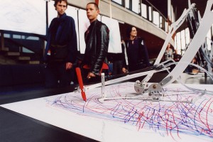
Its ‘brain’ of dissociated rat neurons is cultured on an MEA in our lab in Atlanta while the geographically detached ‘body’ lives in Perth. The body itself is a set of pneumatically actuated robotic arms moving pens on a piece of paper …

A camera located above the workspace captures the progress of drawings created by the neurally-controlled movement of the arms. The visual data then instructed stimulation frequencies for the 60 electrodes on the MEA.

The brain and body talk through the internet over TCP/IP in real time providing closed loop communication for a neurally controlled ‘semi-living artist’. We see this as a medium from which to address various scientific, philosophical, and artistic questions.

Getting back to SymbioticA, my most recent mention of them was in a Dec. 28, 2011 posting about Boo Chapple’s (resident at SymbioticA) Transjuicer installation at Dublin’s Science Gallery (I’ve excerpted a portion of an interview with Chapple where she describes what she’s doing),

I’m not sure that Transjuicer is so much about science as it is about belief, the economy of human-animal relations, and the politics of material transformation.

On that note I leave you with these fish and chips (from the Wikipedia essay about the menu item Fish and Chips),

Cod and chips in Horseshoe Bay, B.C., Canada, December 2010. Credit: Robin Miller

Are we creating a Star Trek world? T-rays and tricorders

There’s been quite a flutter online (even the Huffington Post has published a piece) about ‘Star Trek-hand-held medical scanners’ becoming possible due to some recent work in the area of T-rays. From the Jan. 20, 2012 news item on Nanowerk,

Scientists who have developed a new way to create a type of radiation known as Terahertz (THz) or T-rays – the technology behind full-body security scanners – say their new, stronger and more efficient continuous wave T-rays could be used to make better medical scanning gadgets and may one day lead to innovations similar to the “tricorder” scanner used in Star Trek.

In a study published recently in Nature Photonics (“Greatly enhanced continuous-wave terahertz emission by nano-electrodes in a photoconductive photomixer” [behind a paywall]), researchers from the Institute of Materials Research and Engineering (IMRE), a research institute of the Agency for Science, Technology and Research (A*STAR) in Singapore and Imperial College London in the UK have made T-rays into a much stronger directional beam than was previously thought possible and have efficiently produced T-rays at room-temperature conditions. This breakthrough allows future T-ray systems to be smaller, more portable, easier to operate, and much cheaper.

For anyone who’s not familiar with ‘Star Trek world’ and tricorders, here’s a brief description from a Wikipedia essay about tricorders,

In the fictional Star Trek universe, a tricorder is a multifunction handheld device used for sensor scanning, data analysis, and recording data.

David Freeman in his Jan. 21, 2012 article for the Huffington Post about the research puts it this way,

Trekkies, take heart. A scientific breakthrough involving a form of infrared radiation known as terahertz (THz) waves could lead to handheld medical scanners reminiscent of the “tricorder” featured on the original Star Trek television series.

What’s the breakthrough? Using nanotechnology, physicists in London and Singapore found a way to make a beam of the”T-rays”–which are now used in full-body airport security scanners–stronger and more directional.

Here’s how the improved T-ray technology works (from the Jan. 20, 2012 news item on Nanowerk),

In the new technique, the researchers demonstrated that it is possible to produce a strong beam of T-rays by shining light of differing wavelengths on a pair of electrodes – two pointed strips of metal separated by a 100 nanometre gap on top of a semiconductor wafer. The unique tip-to-tip nano-sized gap electrode structure greatly enhances the THz field and acts like a nano-antenna that amplifies the THz wave generated. The waves are produced by an interaction between the electromagnetic waves of the light pulses and a powerful current passing between the semiconductor electrodes from the carriers generated in the underlying semiconductor. The scientists are able to tune the wavelength of the T-rays to create a beam that is useable in the scanning technology.

Lead author Dr Jing Hua Teng, from A*STAR’s IMRE, said: “The secret behind the innovation lies in the new nano-antenna that we had developed and integrated into the semiconductor chip.” ….

Research co-author Stefan Maier, a Visiting Scientist at A*STAR’s IMRE and Professor in the Department of Physics at Imperial College London, said: “T-rays promise to revolutionise medical scanning to make it faster and more convenient, potentially relieving patients from the inconvenience of complicated diagnostic procedures and the stress of waiting for accurate results. Thanks to modern nanotechnology and nanofabrication, we have made a real breakthrough in the generation of T-rays that takes us a step closer to these new scanning devices. …”

It’s another story about handheld (or point-of-care) diagnostic devices and I have posted on this topic previously:

  • Jan. 4, 2012 about work in Alberta;
  •  Dec. 22, 2011 on grants to scientists in the US and Canada working on these devices;
  •  Aug. 4, 2011 about a diagnostic device the size of a credit card;
  •  Mar. 1, 2011 about nanoLAB from Stanford University (my last sentence in that posting “It’s not quite Star Trek yet but we’re getting there.”); and,
  •  Feb. 5, 2011 about the Argento and PROOF initiatives.

I see I had four articles last year and this year (one month old), I already have two articles on these devices. It reflects my own interest, as well as, the amount work being done in this area.