Tag Archives: atomic force microscope (AFM)

Nanotechnology book suggestions for 2020

A January 23, 2020 news item on Nanowerk features a number of new books. Here are summaries of a couple of them from the news item (Note: Links have been removed),

The main goal of “Nanotechnology in Skin, Soft Tissue, and Bone Infections” is to deal with the role of nanobiotechnology in skin, soft tissue and bone infections since it is difficult to treat the infections due to the development of resistance in them against existing antibiotics.

The present interdisciplinary book is very useful for a diverse group of readers including nanotechnologists, medical microbiologists, dermatologists, osteologists, biotechnologists, bioengineers.

Nanotechnology in Skin, Soft-Tissue, and Bone Infections” is divided into four sections: Section I- includes role of nanotechnology in skin infections such as atopic dermatitis, and nanomaterials for combating infections caused by bacteria and fungi. Section II- incorporates how nanotechnology can be used for soft-tissue infections such as diabetic foot ulcer and other wound infections; Section III- discusses about the nanomaterials in artificial scaffolds bone engineering and bone infections caused by bacteria and fungi; and also about the toxicity issues generated by the nanomaterials in general and nanoparticles in particular.

Advanced Materials for Defense: Development, Analysis and Applications” is a collection of high quality research and review papers submitted to the 1st World Conference on Advanced Materials for Defense (AUXDEFENSE 2018).

A wide range of topics related to the defense area such as ballistic protection, impact and energy absorption, composite materials, smart materials and structures, nanomaterials and nano structures, CBRN protection, thermoregulation, camouflage, auxetic materials, and monitoring systems is covered.

Written by the leading experts in these subjects, this work discusses both technological advances in terms of materials as well as product designing, analysis as well as case studies.

This volume will prove to be a valuable resource for researchers and scientists from different engineering disciplines such as materials science, chemical engineering, biological sciences, textile engineering, mechanical engineering, environmental science, and nanotechnology.

Nanoengineering is a branch of engineering that exploits the unique properties of nanomaterials—their size and quantum effects—and the interaction between these materials, in order to design and manufacture novel structures and devices that possess entirely new functionality and capabilities, which are not obtainable by macroscale engineering.

While the term nanoengineering is often used synonymously with the general term nanotechnology, the former technically focuses more closely on the engineering aspects of the field, as opposed to the broader science and general technology aspects that are encompassed by the latter.

Nanoengineering: The Skills and Tools Making Technology Invisible” puts a spotlight on some of the scientists who are pushing the boundaries of technology and it gives examples of their work and how they are advancing knowledge one little step at a time.

This book is a collection of essays about researchers involved in nanoengineering and many other facets of nanotechnologies. This research involves truly multidisciplinary and international efforts, covering a wide range of scientific disciplines such as medicine, materials sciences, chemistry, toxicology, biology and biotechnology, physics and electronics.

The book showcases 176 very specific research projects and you will meet the scientists who develop the theories, conduct the experiments, and build the new materials and devices that will make nanoengineering a core technology platform for many future products and applications.

On January 28, 2020, Azonano featured a book review for “Nano Comes to Life: How Nanotechnology is Transforming Medicine and the Future of Biology.” The review by Rebecca Megson-Smith, marketing lead, was originally published on the NuNano company blog

Covering sciences ‘greatest hits’ since we have been able to look at the world on the nanoscale, as well as where it is taking our understanding of life, Nano Comes to Life: How Nanotechnology is Transforming Medicine and the Future of Biology is an inspiring and joyful read.

As author Sonia Contera writes, biology is an area of intense interest and study. With the advent of nanotechnology, a more diverse range of scientists from across the disciplines are now coming together to solve some of the biggest issues of our time.

The ability to visualise, interact with, manipulate and create matter at the nanometer scale – the level of molecules, proteins and DNA – combined with the physicists quantitative and mathematical approach is revolutionising our understanding of the complexity which underpins life.

I particularly enjoyed the section that discussed the history of scanning tools. Here Contera highlights how profoundly the development of the STM [scanning tunneling microscope] transformed human interaction with matter.

Not only did it image at the atomic level with ‘unprecedented accuracy using a relatively simple, cheap tool’, but the STM was able to pick up and move the atoms around one by one. And what it couldn’t do effectively – work within the biological environments – was and is achievable through the introduction of the AFM [atomic force microscope].

She [Contera] writes:

“Physics urges us to consider life as a whole emergent from the greater whole – emanating from the same rules that govern the entire cosmos.”

I leave you with another bold declaration from Sonia about the good that the merging of the sciences has offered and, on behalf of everyone at NuNano, would like to wish you all a very Merry Christmas and Happy New Year – see you in 2020!

“As physics, engineering, computer science and materials science merge with biology, they are actually helping to reconnect science and technology with the deep questions that humans have asked themselves from the beginning of civilization: What is life? What does it mean to be human when we can manipulate and even exploit our own biology?”

Sonia Contera is professor of biological physics in the Department of Physics at the University of Oxford. She is a leading pioneer in the field of nanotechnology.

Megson-Smith certainly seems enthused about the book and she reminded me of how interested I was in STMs and AFMs when I first started investigating and writing about nanotechnology. Given the review but not having seen the book myself, it seems this might be a good introduction.

My introductory book was the 2009 Soft Machines: Nanotechnology and Life by Richard Jones, a professor of physics and astronomy at the University of Sheffield. I have great affection for the book and, if memory serves, it hasn’t really aged. One more thing, Jones can be very funny. It’s not many people who can successfully combine humour and nanotechnology.

You can find Megson-Smith’s original posting here.
Getting a more complete picture of aerosol particles at the nanoscale

What is in the air we breathe? In addition to the gases we learned about in school there are particles, not just the dust particles you can see, but micro- and nanoparticles too and scientists would like to know more about them.

An August 23, 2017 news item on Nanowerk features work which may help scientists in their quest,

They may be tiny and invisible, says Xiaoji Xu, but the aerosol particles suspended in gases play a role in cloud formation and environmental pollution and can be detrimental to human health.

Aerosol particles, which are found in haze, dust and vehicle exhaust, measure in the microns. One micron is one-millionth of a meter; a thin human hair is about 30 microns thick.

The particles, says Xu, are among the many materials whose chemical and mechanical properties cannot be fully measured until scientists develop a better method of studying materials at the microscale as well as the much smaller nanoscale (1 nm is one-billionth of a meter).

Xu, an assistant professor of chemistry, has developed such a method and utilized it to perform noninvasive chemical imaging of a variety of materials, as well as mechanical mapping with a spatial resolution of 10 nanometers.

The technique, called peak force infrared (PFIR) microscopy, combines spectroscopy and scanning probe microscopy. In addition to shedding light on aerosol particles, Xu says, PFIR will help scientists study micro- and nanoscale phenomena in a variety of inhomogeneous materials.

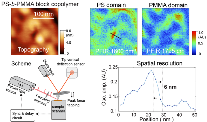
The lower portion of this image by Xiaoji Xu’s group shows the operational scheme of peak force infrared (PFIR) microscopy. The upper portion shows the topography of nanoscale PS-b-PMMA polymer islands on a gold substrate. (Image courtesy of Xiaoji Xu)

An August 22, 2017 Lehih University news release by Kurt Pfitzer (also on EurekAlert), which originated the news item, explains the research in more detail (Note: A link has been removed),

“Materials in nature are rarely homogeneous,” says Xu. “Functional polymer materials often consist of nanoscale domains that have specific tasks. Cellular membranes are embedded with proteins that are nanometers in size. Nanoscale defects of materials exist that affect their mechanical and chemical properties.

“PFIR microscopy represents a fundamental breakthrough that will enable multiple innovations in areas ranging from the study of aerosol particles to the investigation of heterogeneous and biological materials,” says Xu.

Xu and his group recently reported their results in an article titled “Nanoscale simultaneous chemical and mechanical imaging via peak force infrared microscopy.” The article was published in Science Advances, a journal of the American Association for the Advancement of Science, which also publishes Science magazine.

The article’s lead author is Le Wang, a Ph.D. student at Lehigh. Coauthors include Xu and Lehigh Ph.D. students Haomin Wang and Devon S. Jakob, as well as Martin Wagner of Bruker Nano in Santa Barbara, Calif., and Yong Yan of the New Jersey Institute of Technology.

“PFIR microscopy enables reliable chemical imaging, the collection of broadband spectra, and simultaneous mechanical mapping in one simple setup with a spatial resolution of ~10 nm,” the group wrote.

“We have investigated three types of representative materials, namely, soft polymers, perovskite crystals and boron nitride nanotubes, all of which provide a strong PFIR resonance for unambiguous nanochemical identification. Many other materials should be suited as well for the multimodal characterization that PFIR microscopy has to offer.

“In summary, PFIR microscopy will provide a powerful analytical tool for explorations at the nanoscale across wide disciplines.”

Xu and Le Wang also published a recent article about the use of PFIR to study aerosols. Titled “Nanoscale spectroscopic and mechanical characterization of individual aerosol particles using peak force infrared microscopy,” the article appeared in an “Emerging Investigators” issue of Chemical Communications, a journal of the Royal Society of Chemistry. Xu was featured as one of the emerging investigators in the issue. The article was coauthored with researchers from the University of Macau and the City University of Hong Kong, both in China.

PFIR simultaneously obtains chemical and mechanical information, says Xu. It enables researchers to analyze a material at various places, and to determine its chemical compositions and mechanical properties at each of these places, at the nanoscale.

“A material is not often homogeneous,” says Xu. “Its mechanical properties can vary from one region to another. Biological systems such as cell walls are inhomogeneous, and so are materials with defects. The features of a cell wall measure about 100 nanometers in size, placing them well within range of PFIR and its capabilities.”

PFIR has several advantages over scanning near-field optical microscopy (SNOM), the current method of measuring material properties, says Xu. First, PFIR obtains a fuller infrared spectrum and a sharper image—6-nm spatial resolution—of a wider variety of materials than does SNOM. SNOM works well with inorganic materials, but does not obtain as strong an infrared signal as the Lehigh technique does from softer materials such as polymers or biological materials.

“Our technique is more robust,” says Xu. “It works better with soft materials, chemical as well as biological.”

The second advantage of PFIR is that it can perform what Xu calls point spectroscopy.

“If there is something of interest chemically on a surface,” Xu says, “I put an AFM [atomic force microscopy] probe to that location to measure the peak-force infrared response.

“It is very difficult to obtain these spectra with current scattering-type scanning near-field optical microscopy. It can be done, but it requires very expensive light sources. Our method uses a narrow-band infrared laser and costs about $100,000. The existing method uses a broadband light source and costs about $300,000.”

A third advantage, says Xu, is that PFIR obtains a mechanical as well as a chemical response from a material.

“No other spectroscopy method can do this,” says Xu. “Is a material rigid or soft? Is it inhomogeneous—is it soft in one area and rigid in another? How does the composition vary from the soft to the rigid areas? A material can be relatively rigid and have one type of chemical composition in one area, and be relatively soft with another type of composition in another area.

“Our method simultaneously obtains chemical and mechanical information. It will be useful for analyzing a material at various places and determining its compositions and mechanical properties at each of these places, at the nanoscale.”

A fourth advantage of PFIR is its size, says Xu.

“We use a table-top laser to get infrared spectra. Ours is a very compact light source, as opposed to the much larger sizes of competing light sources. Our laser is responsible for gathering information concerning chemical composition. We get mechanical information from the AFM [atomic force microscope]. We integrate the two types of measurements into one device to simultaneously obtain two channels of information.”

Although PFIR does not work with liquid samples, says Xu, it can measure the properties of dried biological samples, including cell walls and protein aggregates, achieving a 10-nm spatial resolution without staining or genetic modification.

This looks like very exciting work.

Here are links and citations for both studies mentioned in the news release (the most recently published being cited first),

Nanoscale simultaneous chemical and mechanical imaging via peak force infrared microscopy by Le Wang, Haomin Wang, Martin Wagner, Yong Yan, Devon S. Jakob, and Xiaoji G. Xu. Science Advances 23 Jun 2017: Vol. 3, no. 6, e1700255 DOI: 10.1126/sciadv.1700255

Nanoscale spectroscopic and mechanical characterization of individual aerosol particles using peak force infrared microscopy by Le Wang, Dandan Huang, Chak K. Chan, Yong Jie Li, and Xiaoji G. Xu. Chem. Commun., 2017,53, 7397-7400 DOI: 10.1039/C7CC02301D First published on 16 Jun 2017

The June 23, 2017 paper is open access while the June 16, 2017 paper is behind a paywall.

Atomic force microscope with nanowire sensors

Measuring the size and direction of forces may become reality with a nanotechnology-enabled atomic force microscope designed by Swiss scientists, according to an Oct. 17, 2016 news item on phys.org,

A new type of atomic force microscope (AFM) uses nanowires as tiny sensors. Unlike standard AFM, the device with a nanowire sensor enables measurements of both the size and direction of forces. Physicists at the University of Basel and at the EPF Lausanne have described these results in the recent issue of Nature Nanotechnology.

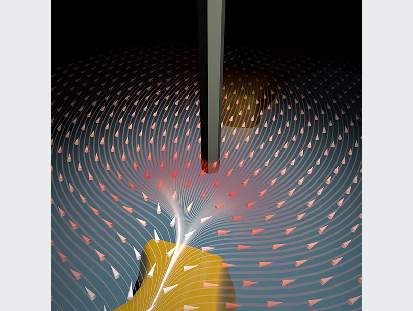
A nanowire sensor measures size and direction of forces (Image: University of Basel, Department of Physics)

A nanowire sensor measures size and direction of forces (Image: University of Basel, Department of Physics)

An Oct. 17, 2016 University of Basel press release (also on EurekAlert), which originated the news item, expands on the theme,

Nanowires are extremely tiny filamentary crystals which are built-up molecule by molecule from various materials and which are now being very actively studied by scientists all around the world because of their exceptional properties.

The wires normally have a diameter of 100 nanometers and therefore possess only about one thousandth of a hair thickness. Because of this tiny dimension, they have a very large surface in comparison to their volume. This fact, their small mass and flawless crystal lattice make them very attractive in a variety of nanometer-scale sensing applications, including as sensors of biological and chemical samples, and as pressure or charge sensors.

Measurement of direction and size

The team of Argovia Professor Martino Poggio from the Swiss Nanoscience Institute (SNI) and the Department of Physics at the University of Basel has now demonstrated that nanowires can also be used as force sensors in atomic force microscopes. Based on their special mechanical properties, nanowires vibrate along two perpendicular axes at nearly the same frequency. When they are integrated into an AFM, the researchers can measure changes in the perpendicular vibrations caused by different forces. Essentially, they use the nanowires like tiny mechanical compasses that point out both the direction and size of the surrounding forces.

Image of the two-dimensional force field

The scientists from Basel describe how they imaged a patterned sample surface using a nanowire sensor. Together with colleagues from the EPF Lausanne, who grew the nanowires, they mapped the two-dimensional force field above the sample surface using their nanowire “compass”. As a proof-of-principle, they also mapped out test force fields produced by tiny electrodes.

The most challenging technical aspect of the experiments was the realization of an apparatus that could simultaneously scan a nanowire above a surface and monitor its vibration along two perpendicular directions. With their study, the scientists have demonstrated a new type of AFM that could extend the technique’s numerous applications even further.

AFM – today widely used

The development of AFM 30 years ago was honored with the conferment of the Kavli-Prize [2016 Kavli Prize in Nanoscience] beginning of September this year. Professor Christoph Gerber of the SNI and Department of Physics at the University of Basel is one of the awardees, who has substantially contributed to the wide use of AFM in different fields, including solid-state physics, materials science, biology, and medicine.

The various different types of AFM are most often carried out using cantilevers made from crystalline Si as the mechanical sensor. “Moving to much smaller nanowire sensors may now allow for even further improvements on an already amazingly successful technique”, Martino Poggio comments his approach.

I featured an interview article with Christoph Gerber and Gerd Binnig about their shared Kavli prize and about inventing the AFM in a Sept. 20, 2016 posting.

As for the latest innovation, here’s a link to and a citation for the paper,

Vectorial scanning force microscopy using a nanowire sensor by Nicola Rossi, Floris R. Braakman, Davide Cadeddu, Denis Vasyukov, Gözde Tütüncüoglu, Anna Fontcuberta i Morral, & Martino Poggio. Nature Nanotechnology (2016) doi:10.1038/nnano.2016.189 Published online 17 October 2016

This paper is behind a paywall.