Tag Archives: bottom-up engineering

Why can’t they produce graphene at usable (industrial) scales?

Kevin Wyss, PhD chemistry student at Rice University, has written an explanation of why graphene is not produced in quantities that make it usable in industry in his November 29, 2022 essay for The Conversation (h/t Nov. 29, 2022 phys.org news item), Note: Links have been removed from the following,

“Future chips may be 10 times faster, all thanks to graphene”; “Graphene may be used in COVID-19 detection”; and “Graphene allows batteries to charge 5x faster” – those are just a handful of recent dramatic headlines lauding the possibilities of graphene. Graphene is an incredibly light, strong and durable material made of a single layer of carbon atoms. With these properties, it is no wonder researchers have been studying ways that graphene could advance material science and technology for decades.

Graphene is a fascinating material, just as the sensational headlines suggest, but it is only just starting be used in real-world applications. The problem lies not in graphene’s properties, but in the fact that it is still incredibly difficult and expensive to manufacture at commercial scales.

Wyss highlights the properties that make graphene so attractive, from the November 29, 2022 essay (Note: Links have been removed from the following),

… The material can be used to create flexible electronics and to purify or desalinate water. And adding just 0.03 ounces (1 gram) of graphene to 11.5 pounds (5 kilograms) of cement increases the strength of the cement by 35%.

As of late 2022, Ford Motor Co., with which I worked as part of my doctoral research, is one of the the only companies to use graphene at industrial scales. Starting in 2018, Ford began making plastic for its vehicles that was 0.5% graphene – increasing the plastic’s strength by 20%.

There are two ways of producing graphene as Wyss notes in his November 29, 2022 essay (Note: Links have been removed from the following),

Top-down synthesis [emphasis mine], also known as graphene exfoliation, works by peeling off the thinnest possible layers of carbon from graphite. Some of the earliest graphene sheets were made by using cellophane tape to peel off layers of carbon from a larger piece of graphite.

The problem is that the molecular forces holding graphene sheets together in graphite are very strong, and it’s hard to pull sheets apart. Because of this, graphene produced using top-down methods is often many layers thick, has holes or deformations, and can contain impurities. Factories can produce a few tons of mechanically or chemically exfoliated graphene per year, and for many applications – like mixing it into plastic – the lower-quality graphene works well.

Bottom-up synthesis [emphasis mine] builds the carbon sheets one atom at a time over a few hours. This process – called vapor deposition – allows researchers to produce high-quality graphene that is one atom thick and up to 30 inches across. This yields graphene with the best possible mechanical and electrical properties. The problem is that with a bottom-up synthesis, it can take hours to make even 0.00001 gram – not nearly fast enough for any large scale uses like in flexible touch-screen electronics or solar panels, for example.

Current production methods of graphene, both top-down and bottom-up, are expensive as well as energy and resource intensive, and simply produce too little product, too slowly.

Wyss has written an informative essay and, for those who need it, he has included an explanation of the substance known as graphene.

A new generation of xenobots made with frog cells

I meant to feature this work last year when it was first announced so I’m delighted a second chance has come around so soon after. From a March 31, 2021 news item on ScienceDaily,

Last year, a team of biologists and computer scientists from Tufts University and the University of Vermont (UVM) created novel, tiny self-healing biological machines from frog cells called “Xenobots” that could move around, push a payload, and even exhibit collective behavior in the presence of a swarm of other Xenobots.

Get ready for Xenobots 2.0.

Here’s a video of the Xenobot 2.0. It’s amazing but, for anyone who has problems with animal experimentation, this may be disturbing,


The next version of Xenobots have been created – they’re faster, live longer, and can now record information. (Source: Doug Blackiston & Emma Lederer)

A March 31, 2021 Tufts University news release by Mike Silver (also on EurekAlert and adapted and published as Scientists Create the Next Generation of Living Robots on the University of Vermont website as a UVM Today story),

The same team has now created life forms that self-assemble a body from single cells, do not require muscle cells to move, and even demonstrate the capability of recordable memory. The new generation Xenobots also move faster, navigate different environments, and have longer lifespans than the first edition, and they still have the ability to work together in groups and heal themselves if damaged. The results of the new research were published today [March 31, 2021] in Science Robotics.

Compared to Xenobots 1.0, in which the millimeter-sized automatons were constructed in a “top down” approach by manual placement of tissue and surgical shaping of frog skin and cardiac cells to produce motion, the next version of Xenobots takes a “bottom up” approach. The biologists at Tufts took stem cells from embryos of the African frog Xenopus laevis (hence the name “Xenobots”) and allowed them to self-assemble and grow into spheroids, where some of the cells after a few days differentiated to produce cilia – tiny hair-like projections that move back and forth or rotate in a specific way. Instead of using manually sculpted cardiac cells whose natural rhythmic contractions allowed the original Xenobots to scuttle around, cilia give the new spheroidal bots “legs” to move them rapidly across a surface. In a frog, or human for that matter, cilia would normally be found on mucous surfaces, like in the lungs, to help push out pathogens and other foreign material. On the Xenobots, they are repurposed to provide rapid locomotion. 

“We are witnessing the remarkable plasticity of cellular collectives, which build a rudimentary new ‘body’ that is quite distinct from their default – in this case, a frog – despite having a completely normal genome,” said Michael Levin, Distinguished Professor of Biology and director of the Allen Discovery Center at Tufts University, and corresponding author of the study. “In a frog embryo, cells cooperate to create a tadpole. Here, removed from that context, we see that cells can re-purpose their genetically encoded hardware, like cilia, for new functions such as locomotion. It is amazing that cells can spontaneously take on new roles and create new body plans and behaviors without long periods of evolutionary selection for those features.”

“In a way, the Xenobots are constructed much like a traditional robot.  Only we use cells and tissues rather than artificial components to build the shape and create predictable behavior.” said senior scientist Doug Blackiston, who co-first authored the study with research technician Emma Lederer. “On the biology end, this approach is helping us understand how cells communicate as they interact with one another during development, and how we might better control those interactions.”

While the Tufts scientists created the physical organisms, scientists at UVM were busy running computer simulations that modeled different shapes of the Xenobots to see if they might exhibit different behaviors, both individually and in groups. Using the Deep Green supercomputer cluster at UVM’s Vermont Advanced Computing Core, the team, led by computer scientists and robotics experts Josh Bongard and Sam Kriegman, simulated the Xenbots under hundreds of thousands of random environmental conditions using an evolutionary algorithm.  These simulations were used to identify Xenobots most able to work together in swarms to gather large piles of debris in a field of particles

“We know the task, but it’s not at all obvious — for people — what a successful design should look like. That’s where the supercomputer comes in and searches over the space of all possible Xenobot swarms to find the swarm that does the job best,” says Bongard. “We want Xenobots to do useful work. Right now we’re giving them simple tasks, but ultimately we’re aiming for a new kind of living tool that could, for example, clean up microplastics in the ocean or contaminants in soil.” 

It turns out, the new Xenobots are much faster and better at tasks such as garbage collection than last year’s model, working together in a swarm to sweep through a petri dish and gather larger piles of iron oxide particles. They can also cover large flat surfaces, or travel through narrow capillary tubes.

These studies also suggest that the in silico [computer] simulations could in the future optimize additional features of biological bots for more complex behaviors. One important feature added in the Xenobot upgrade is the ability to record information.

Now with memory

A central feature of robotics is the ability to record memory and use that information to modify the robot’s actions and behavior. With that in mind, the Tufts scientists engineered the Xenobots with a read/write capability to record one bit of information, using a fluorescent reporter protein called EosFP, which normally glows green. However, when exposed to light at 390nm wavelength, the protein emits red light instead. 

The cells of the frog embryos were injected with messenger RNA coding for the EosFP protein before stem cells were excised to create the Xenobots. The mature Xenobots now have a built-in fluorescent switch which can record exposure to blue light around 390nm.
The researchers tested the memory function by allowing 10 Xenobots to swim around a surface on which one spot is illuminated with a beam of 390nm light. After two hours, they found that three bots emitted red light. The rest remained their original green, effectively recording the “travel experience” of the bots.

This proof of principle of molecular memory could be extended in the future to detect and record not only light but also the presence of radioactive contamination, chemical pollutants, drugs, or a disease condition. Further engineering of the memory function could enable the recording of multiple stimuli (more bits of information) or allow the bots to release compounds or change behavior upon sensation of stimuli. 

“When we bring in more capabilities to the bots, we can use the computer simulations to design them with more complex behaviors and the ability to carry out more elaborate tasks,” said Bongard. “We could potentially design them not only to report conditions in their environment but also to modify and repair conditions in their environment.”

Xenobot, heal thyself

“The biological materials we are using have many features we would like to someday implement in the bots – cells can act like sensors, motors for movement, communication and computation networks, and recording devices to store information,” said Levin. “One thing the Xenobots and future versions of biological bots can do that their metal and plastic counterparts have difficulty doing is constructing their own body plan as the cells grow and mature, and then repairing and restoring themselves if they become damaged. Healing is a natural feature of living organisms, and it is preserved in Xenobot biology.” 

The new Xenobots were remarkably adept at healing and would close the majority of a severe full-length laceration half their thickness within 5 minutes of the injury. All injured bots were able to ultimately heal the wound, restore their shape and continue their work as before. 

Another advantage of a biological robot, Levin adds, is metabolism. Unlike metal and plastic robots, the cells in a biological robot can absorb and break down chemicals and work like tiny factories synthesizing and excreting chemicals and proteins. The whole field of synthetic biology – which has largely focused on reprogramming single celled organisms to produce useful molecules – can now be exploited in these multicellular creatures

Like the original Xenobots, the upgraded bots can survive up to ten days on their embryonic energy stores and run their tasks without additional energy sources, but they can also carry on at full speed for many months if kept in a “soup” of nutrients. 

What the scientists are really after

An engaging description of the biological bots and what we can learn from them is presented in a TED talk by Michael Levin. In his TED Talk, professor Levin describes not only the remarkable potential for tiny biological robots to carry out useful tasks in the environment or potentially in therapeutic applications, but he also points out what may be the most valuable benefit of this research – using the bots to understand how individual cells come together, communicate, and specialize to create a larger organism, as they do in nature to create a frog or human. It’s a new model system that can provide a foundation for regenerative medicine.

Xenobots and their successors may also provide insight into how multicellular organisms arose from ancient single celled organisms, and the origins of information processing, decision making and cognition in biological organisms. 

Recognizing the tremendous future for this technology, Tufts University and the University of Vermont have established the Institute for Computer Designed Organisms (ICDO), to be formally launched in the coming months, which will pull together resources from each university and outside sources to create living robots with increasingly sophisticated capabilities.

The ultimate goal for the Tufts and UVM researchers is not only to explore the full scope of biological robots they can make; it is also to understand the relationship between the ‘hardware’ of the genome and the ‘software’ of cellular communications that go into creating organized tissues, organs and limbs. Then we can gain greater control of that morphogenesis for regenerative medicine, and the treatment of cancer and diseases of aging.

Here’s a link to and a citation for the paper,

A cellular platform for the development of synthetic living machines by Douglas Blackiston, Emma Lederer, Sam Kriegman, Simon Garnier, Joshua Bongard, and Michael Levin. Science Robotics 31 Mar 2021: Vol. 6, Issue 52, eabf1571 DOI: 10.1126/scirobotics.abf1571

This paper is behind a paywall.

Nanobots—at last

Who can resist Etta James? Getting to the point of the post, I’ve been reading about nanobots for years but this is the first time I’ve seen something that resembles what lived in my imagination—at last. From a Sept. 20 , 2017 news item on phys.org (Note: Links have been removed),

Scientists at The University of Manchester have created the world’s first ‘molecular robot’ that is capable of performing basic tasks including building other molecules.

The tiny robots, which are a millionth of a millimetre in size, can be programmed to move and build molecular cargo, using a tiny robotic arm.

Each individual robot is capable of manipulating a single molecule and is made up of just 150 carbon, hydrogen, oxygen and nitrogen atoms. To put that size into context, a billion billion of these robots piled on top of each other would still only be the same size as a single grain of salt.

The robots operate by carrying out chemical reactions in special solutions which can then be controlled and programmed by scientists to perform the basic tasks.

In the future such robots could be used for medical purposes, advanced manufacturing processes and even building molecular factories and assembly lines. …

A Sept. 20, 2017 University of Manchester press release (also on EurekAlert), which originated the news item, provides (perhaps) a little more explanation than is absolutely necessary,

Professor David Leigh, who led the research at University’s School of Chemistry, explains: ‘All matter is made up of atoms and these are the basic building blocks that form molecules. [emphasis mine] Our robot is literally a molecular robot constructed of atoms just like you can build a very simple robot out of Lego bricks. The robot then responds to a series of simple commands that are programmed with chemical inputs by a scientist.

‘It is similar to the way robots are used on a car assembly line. Those robots pick up a panel and position it so that it can be riveted in the correct way to build the bodywork of a car. So, just like the robot in the factory, our molecular version can be programmed to position and rivet components in different ways to build different products, just on a much smaller scale at a molecular level.’

The benefit of having machinery that is so small is it massively reduces demand for materials, can accelerate and improve drug discovery, dramatically reduce power requirements and rapidly increase the miniaturisation of other products. Therefore, the potential applications for molecular robots are extremely varied and exciting.

Prof Leigh says: ‘Molecular robotics represents the ultimate in the miniaturisation of machinery. Our aim is to design and make the smallest machines possible. This is just the start but we anticipate that within 10 to 20 years molecular robots will begin to be used to build molecules and materials on assembly lines in molecular factories.’

Whilst building and operating such tiny machine is extremely complex, the techniques used by the team are based on simple chemical processes.

Prof Leigh added: ‘The robots are assembled and operated using chemistry. This is the science of how atoms and molecules react with each other and how larger molecules are constructed from smaller ones.

‘It is the same sort of process scientists use to make medicines and plastics from simple chemical building blocks. Then, once the nano-robots have been constructed, they are operated by scientists by adding chemical inputs which tell the robots what to do and when, just like a computer program.’

Here’s a link to and a citation for the paper,

Stereodivergent synthesis with a programmable molecular machine by Salma Kassem, Alan T. L. Lee, David A. Leigh, Vanesa Marcos, Leoni I. Palmer, & Simone Pisano. Nature 549,
374–378 (21 September 2017) doi:10.1038/nature23677 Published online 20 September 2017

This paper is behind a paywall.

There’s a rather attractive image accompanying the news release which manages to be both quite informative and wholly unrealistic,

Courtesy: University of Manchester

Nanobots first made their way into popular science with K. Eric Drexler’s book 1986, Engines of Creation, which also provoked a spirited academic debate. See Drexler’s Wikipedia entry for more. One final comment, this would seem to be a promising start to the long-held dream of bottom-up engineering of materials.

‘Smart’ fabric that’s bony

Researchers at Australia’s University of New South of Wales (UNSW) have devised a means of ‘weaving’ a material that mimics *bone tissue, periosteum according to a Jan. 11, 2017 news item on ScienceDaily,

For the first time, UNSW [University of New South Wales] biomedical engineers have woven a ‘smart’ fabric that mimics the sophisticated and complex properties of one nature’s ingenious materials, the bone tissue periosteum.

Having achieved proof of concept, the researchers are now ready to produce fabric prototypes for a range of advanced functional materials that could transform the medical, safety and transport sectors. Patents for the innovation are pending in Australia, the United States and Europe.

Potential future applications range from protective suits that stiffen under high impact for skiers, racing-car drivers and astronauts, through to ‘intelligent’ compression bandages for deep-vein thrombosis that respond to the wearer’s movement and safer steel-belt radial tyres.

A Jan. 11, 2017 UNSW press release on EurekAlert, which originated the news item, expands on the theme,

Many animal and plant tissues exhibit ‘smart’ and adaptive properties. One such material is the periosteum, a soft tissue sleeve that envelops most bony surfaces in the body. The complex arrangement of collagen, elastin and other structural proteins gives periosteum amazing resilience and provides bones with added strength under high impact loads.

Until now, a lack of scalable ‘bottom-up’ approaches by researchers has stymied their ability to use smart tissues to create advanced functional materials.

UNSW’s Paul Trainor Chair of Biomedical Engineering, Professor Melissa Knothe Tate, said her team had for the first time mapped the complex tissue architectures of the periosteum, visualised them in 3D on a computer, scaled up the key components and produced prototypes using weaving loom technology.

“The result is a series of textile swatch prototypes that mimic periosteum’s smart stress-strain properties. We have also demonstrated the feasibility of using this technique to test other fibres to produce a whole range of new textiles,” Professor Knothe Tate said.

In order to understand the functional capacity of the periosteum, the team used an incredibly high fidelity imaging system to investigate and map its architecture.

“We then tested the feasibility of rendering periosteum’s natural tissue weaves using computer-aided design software,” Professor Knothe Tate said.

The computer modelling allowed the researchers to scale up nature’s architectural patterns to weave periosteum-inspired, multidimensional fabrics using a state-of-the-art computer-controlled jacquard loom. The loom is known as the original rudimentary computer, first unveiled in 1801.

“The challenge with using collagen and elastin is their fibres, that are too small to fit into the loom. So we used elastic material that mimics elastin and silk that mimics collagen,” Professor Knothe Tate said.

In a first test of the scaled-up tissue weaving concept, a series of textile swatch prototypes were woven, using specific combinations of collagen and elastin in a twill pattern designed to mirror periosteum’s weave. Mechanical testing of the swatches showed they exhibited similar properties found in periosteum’s natural collagen and elastin weave.

First author and biomedical engineering PhD candidate, Joanna Ng, said the technique had significant implications for the development of next-generation advanced materials and mechanically functional textiles.

While the materials produced by the jacquard loom have potential manufacturing applications – one tyremaker believes a titanium weave could spawn a new generation of thinner, stronger and safer steel-belt radials – the UNSW team is ultimately focused on the machine’s human potential.

“Our longer term goal is to weave biological tissues – essentially human body parts – in the lab to replace and repair our failing joints that reflect the biology, architecture and mechanical properties of the periosteum,” Ms Ng said.

An NHMRC development grant received in November [2016] will allow the team to take its research to the next phase. The researchers will work with the Cleveland Clinic and the University of Sydney’s Professor Tony Weiss to develop and commercialise prototype bone implants for pre-clinical research, using the ‘smart’ technology, within three years.

In searching for more information about this work, I found a Winter 2015 article (PDF; pp. 8-11) by Amy Coopes and Steve Offner for UNSW Magazine about Knothe Tate and her work (Note: In Australia, winter would be what we in the Northern Hemisphere consider summer),

Tucked away in a small room in UNSW’s Graduate School of Biomedical Engineering sits a 19th century–era weaver’s wooden loom. Operated by punch cards and hooks, the machine was the first rudimentary computer when it was unveiled in 1801. While on the surface it looks like a standard Jacquard loom, it has been enhanced with motherboards integrated into each of the loom’s five hook modules and connected to a computer. This state-of-the-art technology means complex algorithms control each of the 5,000 feed-in fibres with incredible precision.

That capacity means the loom can weave with an extraordinary variety of substances, from glass and titanium to rayon and silk, a development that has attracted industry attention around the world.

The interest lies in the natural advantage woven materials have over other manufactured substances. Instead of manipulating material to create new shades or hues as in traditional weaving, the fabrics’ mechanical properties can be modulated, to be stiff at one end, for example, and more flexible at the other.

“Instead of a pattern of colours we get a pattern of mechanical properties,” says Melissa Knothe Tate, UNSW’s Paul Trainor Chair of Biomedical Engineering. “Think of a rope; it’s uniquely good in tension and in bending. Weaving is naturally strong in that way.”


The interface of mechanics and physiology is the focus of Knothe Tate’s work. In March [2015], she travelled to the United States to present another aspect of her work at a meeting of the international Orthopedic Research Society in Las Vegas. That project – which has been dubbed “Google Maps for the body” – explores the interaction between cells and their environment in osteoporosis and other degenerative musculoskeletal conditions such as osteoarthritis.

Using previously top-secret semiconductor technology developed by optics giant Zeiss, and the same approach used by Google Maps to locate users with pinpoint accuracy, Knothe Tate and her team have created “zoomable” anatomical maps from the scale of a human joint down to a single cell.

She has also spearheaded a groundbreaking partnership that includes the Cleveland Clinic, and Brown and Stanford universities to help crunch terabytes of data gathered from human hip studies – all processed with the Google technology. Analysis that once took 25 years can now be done in a matter of weeks, bringing researchers ever closer to a set of laws that govern biological behaviour. [p. 9]

I gather she was recruited from the US to work at the University of New South Wales and this article was to highlight why they recruited her and to promote the university’s biomedical engineering department, which she chairs.

Getting back to 2017, here’s a link to and citation for the paper,

Scale-up of nature’s tissue weaving algorithms to engineer advanced functional materials by Joanna L. Ng, Lillian E. Knothe, Renee M. Whan, Ulf Knothe & Melissa L. Knothe Tate. Scientific Reports 7, Article number: 40396 (2017) doi:10.1038/srep40396 Published online: 11 January 2017

This paper is open access.

One final comment, that’s a lot of people (three out of five) with the last name Knothe in the author’s list for the paper.

*’the bone tissue’ changed to ‘bone tissue’ on July 17,2017.

Kinetic properties of cement at the nanoscale

There was a Vancouver-born architect, Arthur Erickson, who adored concrete as a building material. In fact, he gained an international reputation for his ‘concrete’ work. I have never been a fan, especially after attending Simon Fraser University (one of Erickson’s early triumphs) in Vancouver (Canada) and experiencing the joy of deteriorating concrete structures.

This somewhat related news concerns cement, (from a Dec.7, 2016 news item on ScienceDaily,

Bringing order to disorder is key to making stronger and greener cement, the paste that binds concrete.

Scientists at Rice University have decoded the kinetic properties of cement and developed a way to “program” the microscopic, semicrystalline particles within. The process turns particles from disordered clumps into regimented cubes, spheres and other forms that combine to make the material less porous and more durable.

A Dec. 7, 2016 Rice University news release, which originated the news item, explains further (Note: Links have been removed),

The technique may lead to stronger structures that require less concrete – and less is better, said Rice materials scientist and lead author Rouzbeh Shahsavari. Worldwide production of more than 3 billion tons of concrete a year now emits as much as 10 percent of the carbon dioxide, a greenhouse gas, released to the atmosphere.

Through extensive experiments, Shahsavari and his colleagues decoded the nanoscale reactions — or “morphogenesis” — of the crystallization within calcium-silicate hydrate (C-S-H) cement that holds concrete together.

For the first time, they synthesized C-S-H particles in a variety of shapes, including cubes, rectangular prisms, dendrites, core-shells and rhombohedra and mapped them into a unified morphology diagram for manufacturers and builders who wish to engineer concrete from the bottom up.

“We call it programmable cement,” he said. “The great advance of this work is that it’s the first step in controlling the kinetics of cement to get desired shapes. We show how one can control the morphology and size of the basic building blocks of C-S-H so that they can self-assemble into microstructures with far greater packing density compared with conventional amorphous C-S-H microstructures.”

He said the idea is akin to the self-assembly of metallic crystals and polymers. “It’s a hot area, and researchers are taking advantage of it,” Shahsavari said. “But when it comes to cement and concrete, it is extremely difficult to control their bottom-up assembly. Our work provides the first recipe for such advanced synthesis.

“The seed particles form first, automatically, in our reactions, and then they dominate the process as the rest of the material forms around them,” he said. “That’s the beauty of it. It’s in situ, seed-mediated growth and does not require external addition of seed particles, as commonly done in the industry to promote crystallization and growth.”

Previous techniques to create ordered crystals in C-S-H required high temperatures or pressures, prolonged reaction times and the use of organic precursors, but none were efficient or environmentally benign, Shahsavari said.

The Rice lab created well-shaped cubes and rectangles by adding small amounts of positive or negative ionic surfactants and calcium silicate to C-S-H and exposing the mix to carbon dioxide and ultrasonic sound. The crystal seeds took shape around surfactant micelles within 25 minutes. Decreasing the calcium silicate yielded more spherical particles and smaller cubes, while increasing it formed clumped spheres and interlocking cubes.

Once the calcite “seeds” form, they trigger the molecules around them to self-assemble into cubes, spheres and other shapes that are orders of magnitude larger. These can pack more tightly together in concrete than amorphous particles, Shahsavari said. Carefully modulating the precursor concentration, temperature and duration of the reaction varies the yield, size and morphology of the final particles.

The discovery is an important step in concrete research, he said. It builds upon his work as part of the Massachusetts Institute of Technology team that decoded cement’s molecular “DNA” in 2009. “There is currently no control over C-S-H shape,” Shahsavari said. “The concrete used today is an amorphous colloid with significant porosity that entails reduced strength and durability.”

Concrete is one focus of Shahsavari’s Rice lab, which has studied both its macroscale manufacture and intrinsic nanoscale properties. Because concrete is the world’s most common construction material and a significant source of atmospheric carbon dioxide, he is convinced of the importance of developing “greener” concrete.

The new technique has several environmental benefits, Shahsavari said. “One is that you need less of it (the concrete) because it is stronger. This stems from better packing of the cubic particles, which leads to stronger microstructures. The other is that it will be more durable. Less porosity makes it harder for unwanted chemicals to find a path through the concrete, so it does a better job of protecting steel reinforcement inside.”

The research required the team to develop a method to test microscopic concrete particles for strength. The researchers used a diamond-tipped nanoindenter to crush single cement particles with a flat edge.

They programmed the indenter to move from one nanoparticle to the next and crush it and gathered mechanical data on hundreds of particles of various shapes in one run. “Other research groups have tested bulk cement and concrete, but no group had ever probed the mechanics of single C-S-H particles and the effect of shape on mechanics of individual particles,” Shahsavari said.

He said strategies developed during the project could have implications for other applications, including bone tissue engineering, drug delivery and refractory materials, and could impact such other complex systems as ceramics and colloids.

Here’s a link to and a citation for the paper,

Morphogenesis of Cement Hydrate by Sakineh E Moghaddam, vahid hejazi, Sung Hoon Hwang, Sreeprasad Srinavasan, Joseph B. Miller, Benhang Shi, Shuo Zhao, Irene Rusakova, Aali R. Alizadeh, Kenton Whitmire and Rouzbeh Shahsavari. J. Mater. Chem. A, 2016, DOI: 10.1039/C6TA09389B First published online 30 Nov 2016

I believe this paper is behind a paywall.

DNA-based nanowires in your computer?

In the quest for smaller and smaller, DNA (deoxyribonucleic acid) is being exploited as never before. From a Nov. 9, 2016 news item on phys.org,

Tinier than the AIDS virus—that is currently the circumference of the smallest transistors. The industry has shrunk the central elements of their computer chips to fourteen nanometers in the last sixty years. Conventional methods, however, are hitting physical boundaries. Researchers around the world are looking for alternatives. One method could be the self-organization of complex components from molecules and atoms. Scientists at the Helmholtz-Zentrum Dresden-Rossendorf (HZDR) and Paderborn University have now made an important advance: the physicists conducted a current through gold-plated nanowires, which independently assembled themselves from single DNA strands. …

A Nov. 9, 2016 HZDR press release (also on EurekAlert), which originated the news item, provides more information,

At first glance, it resembles wormy lines in front of a black background. But what the electron microscope shows up close is that the nanometer-sized structures connect two electrical contacts. Dr. Artur Erbe from the Institute of Ion Beam Physics and Materials Research is pleased about what he sees. “Our measurements have shown that an electrical current is conducted through these tiny wires.” This is not necessarily self-evident, the physicist stresses. We are, after all, dealing with components made of modified DNA. In order to produce the nanowires, the researchers combined a long single strand of genetic material with shorter DNA segments through the base pairs to form a stable double strand. Using this method, the structures independently take on the desired form.

“With the help of this approach, which resembles the Japanese paper folding technique origami and is therefore referred to as DNA-origami, we can create tiny patterns,” explains the HZDR researcher. “Extremely small circuits made of molecules and atoms are also conceivable here.” This strategy, which scientists call the “bottom-up” method, aims to turn conventional production of electronic components on its head. “The industry has thus far been using what is known as the ‘top-down’ method. Large portions are cut away from the base material until the desired structure is achieved. Soon this will no longer be possible due to continual miniaturization.” The new approach is instead oriented on nature: molecules that develop complex structures through self-assembling processes.

Golden Bridges Between Electrodes

The elements that thereby develop would be substantially smaller than today’s tiniest computer chip components. Smaller circuits could theoretically be produced with less effort. There is, however, a problem: “Genetic matter doesn’t conduct a current particularly well,” points out Erbe. He and his colleagues have therefore placed gold-plated nanoparticles on the DNA wires using chemical bonds. Using a “top-down” method – electron beam lithography — they subsequently make contact with the individual wires electronically. “This connection between the substantially larger electrodes and the individual DNA structures have come up against technical difficulties until now. By combining the two methods, we can resolve this issue. We could thus very precisely determine the charge transport through individual wires for the first time,” adds Erbe.

As the tests of the Dresden researchers have shown, a current is actually conducted through the gold-plated wires — it is, however, dependent on the ambient temperature. “The charge transport is simultaneously reduced as the temperature decreases,” describes Erbe. “At normal room temperature, the wires function well, even if the electrons must partially jump from one gold particle to the next because they haven’t completely melded together. The distance, however, is so small that it currently doesn’t even show up using the most advanced microscopes.” In order to improve the conduction, Artur Erbe’s team aims to incorporate conductive polymers between the gold particles. The physicist believes the metallization process could also still be improved.

He is, however, generally pleased with the results: “We could demonstrate that the gold-plated DNA wires conduct energy. We are actually still in the basic research phase, which is why we are using gold rather than a more cost-efficient metal. We have, nevertheless, made an important stride, which could make electronic devices based on DNA possible in the future.”

Here’s a link to and a citation for the paper,

Temperature-Dependent Charge Transport through Individually Contacted DNA Origami-Based Au Nanowires by Bezu Teschome, Stefan Facsko, Tommy Schönherr, Jochen Kerbusch, Adrian Keller, and Artur Erbe. Langmuir, 2016, 32 (40), pp 10159–10165, DOI: 10.1021/acs.langmuir.6b01961, Publication Date (Web): September 14, 2016

Copyright © 2016 American Chemical Society

This paper is behind a paywall.

An examination of nanomanufacturing and nanofabrication

Michael Berger has written an Aug. 11, 2016 Nanowerk Spotlight review of a paper about nanomanufacturing (Note: A link has been removed),

… the path to greater benefits – whether economic, social, or environmental – from nanomanufactured goods and services is not yet clear. A recent review article in ACS Nano (“Nanomanufacturing: A Perspective”) by J. Alexander Liddle and Gregg M. Gallatin, takes silicon integrated circuit manufacturing as a baseline in order to consider the factors involved in matching processes with products, examining the characteristics and potential of top-down and bottom-up processes, and their combination.

The authors also discuss how a careful assessment of the way in which function can be made to follow form can enable high-volume manufacturing of nanoscale structures with the desired useful, and exciting, properties.

Although often used interchangeably, it makes sense to distinguish between nanofabrication and nanomanufacturing using the criterion of economic viability, suggested by the connotations of industrial scale and profitability associated with the word ‘manufacturing’.

Here’s a link to and a citation for the paper Berger is reviewing,

Nanomanufacturing: A Perspective by J. Alexander Liddle and Gregg M. Gallatin. ACS Nano, 2016, 10 (3), pp 2995–3014 DOI: 10.1021/acsnano.5b03299 Publication Date (Web): February 10, 2016

Copyright This article not subject to U.S. Copyright. Published 2016 by the American Chemical Society

This paper is behind a paywall.

Luckily for those who’d like a little more information before purchase, Berger’s review provides some insight into the study additional to what you’ll find in the abstract,

Nanomanufacturing, as the authors define it in their article, therefore, has the salient characteristic of being a source of money, while nanofabrication is often a sink.

To supply some background and indicate the scale of the nanomanufacturing challenge, the figure below shows the selling price ($·m-2) versus the annual production (m2) for a variety of nanoenabled or potentially nanoenabled products. The overall global market sizes are also indicated. It is interesting to note that the selling price spans 5 orders of magnitude, the production six, and the market size three. Although there is no strong correlation between the variables,
market price and size nanoenabled product
Log-log plot of the approximate product selling price ($·m-2) versus global annual production (m2) for a variety of nanoenabled, or potentially nanoenabled products. Approximate market sizes (2014) are shown next to each point. (Reprinted with permission by American Chemical Society)

I encourage anyone interested in nanomanufacturing to read Berger’s article in its entirety as there is more detail and there are more figures to illustrate the points being made. He ends his review with this,

“Perhaps the most exciting prospect is that of creating dynamical nanoscale systems that are capable of exhibiting much richer structures and functionality. Whether this is achieved by learning how to control and engineer biological systems directly, or by building systems based on the same principles, remains to be seen, but will undoubtedly be disruptive and quite probably revolutionary.”

I find the reference to biological systems quite interesting especially in light of the recent launch of DARPA’s (US Defense Advanced Research Projects Agency) Engineered Living Materials (ELM) program (see my Aug. 9, 2016 posting).

Directing self-assembly of multiple molecular patterns within a single material

Self-assembly in this context references the notion of ‘bottom-up engineering’, that is, following nature’s engineering process where elements assemble themselves into a plant, animal, or something else. Humans have for centuries used an approach known as ‘top-down engineering’ where we take materials and reform them, e.g., trees into paper or houses.

Theoretically, bottom-up engineering (self-assembly) is more efficient than top-down engineering but we have yet to become as skilled as Nature at the process.

Scientists at the US Brookhaven National Laboratory believe they have taken a step in the right direction with regard to self-assembly. From an Aug. 8, 2016 Brookhaven National Laboratory news release (also on EurekAlert) by Justin Eure describes the research (Note: A link has been removed),

To continue advancing, next-generation electronic devices must fully exploit the nanoscale, where materials span just billionths of a meter. But balancing complexity, precision, and manufacturing scalability on such fantastically small scales is inevitably difficult. Fortunately, some nanomaterials can be coaxed into snapping themselves into desired formations-a process called self-assembly.

Scientists at the U.S. Department of Energy’s (DOE) Brookhaven National Laboratory have just developed a way to direct the self-assembly of multiple molecular patterns within a single material, producing new nanoscale architectures. The results were published in the journal Nature Communications.

“This is a significant conceptual leap in self-assembly,” said Brookhaven Lab physicist Aaron Stein, lead author on the study. “In the past, we were limited to a single emergent pattern, but this technique breaks that barrier with relative ease. This is significant for basic research, certainly, but it could also change the way we design and manufacture electronics.”

Microchips, for example, use meticulously patterned templates to produce the nanoscale structures that process and store information. Through self-assembly, however, these structures can spontaneously form without that exhaustive preliminary patterning. And now, self-assembly can generate multiple distinct patterns-greatly increasing the complexity of nanostructures that can be formed in a single step.

“This technique fits quite easily into existing microchip fabrication workflows,” said study coauthor Kevin Yager, also a Brookhaven physicist. “It’s exciting to make a fundamental discovery that could one day find its way into our computers.”

The experimental work was conducted entirely at Brookhaven Lab’s Center for Functional Nanomaterials (CFN), a DOE Office of Science User Facility, leveraging in-house expertise and instrumentation.

Cooking up organized complexity

The collaboration used block copolymers-chains of two distinct molecules linked together-because of their intrinsic ability to self-assemble.

“As powerful as self-assembly is, we suspected that guiding the process would enhance it to create truly ‘responsive’ self-assembly,” said study coauthor Greg Doerk of Brookhaven. “That’s exactly where we pushed it.”

To guide self-assembly, scientists create precise but simple substrate templates. Using a method called electron beam lithography-Stein’s specialty-they etch patterns thousands of times thinner than a human hair on the template surface. They then add a solution containing a set of block copolymers onto the template, spin the substrate to create a thin coating, and “bake” it all in an oven to kick the molecules into formation. Thermal energy drives interaction between the block copolymers and the template, setting the final configuration-in this instance, parallel lines or dots in a grid.

“In conventional self-assembly, the final nanostructures follow the template’s guiding lines, but are of a single pattern type,” Stein said. “But that all just changed.”

Lines and dots, living together

The collaboration had previously discovered that mixing together different block copolymers allowed multiple, co-existing line and dot nanostructures to form.

“We had discovered an exciting phenomenon, but couldn’t select which morphology would emerge,” Yager said. But then the team found that tweaking the substrate changed the structures that emerged. By simply adjusting the spacing and thickness of the lithographic line patterns-easy to fabricate using modern tools-the self-assembling blocks can be locally converted into ultra-thin lines, or high-density arrays of nano-dots.

“We realized that combining our self-assembling materials with nanofabricated guides gave us that elusive control. And, of course, these new geometries are achieved on an incredibly small scale,” said Yager.

“In essence,” said Stein, “we’ve created ‘smart’ templates for nanomaterial self-assembly. How far we can push the technique remains to be seen, but it opens some very promising pathways.”

Gwen Wright, another CFN coauthor, added, “Many nano-fabrication labs should be able to do this tomorrow with their in-house tools-the trick was discovering it was even possible.”

The scientists plan to increase the sophistication of the process, using more complex materials in order to move toward more device-like architectures.

“The ongoing and open collaboration within the CFN made this possible,” said Charles Black, director of the CFN. “We had experts in self-assembly, electron beam lithography, and even electron microscopy to characterize the materials, all under one roof, all pushing the limits of nanoscience.”

Here’s a link to and a citation for the paper,

Selective directed self-assembly of coexisting morphologies using block copolymer blends by A. Stein, G. Wright, K. G. Yager, G. S. Doerk, & C. T. Black. Nature Communications 7, Article number: 12366  doi:10.1038/ncomms12366 Published 02 August 2016

This paper is open access.

Book announcement: Atomistic Simulation of Quantum Transport in Nanoelectronic Devices

For anyone who’s curious about where we go after creating chips at the 7nm size, this may be the book for you. Here’s more from a July 27, 2016 news item on Nanowerk,

In the year 2015, Intel, Samsung and TSMC began to mass-market the 14nm technology called FinFETs. In the same year, IBM, working with Global Foundries, Samsung, SUNY, and various equipment suppliers, announced their success in fabricating 7nm devices. A 7nm silicon channel is about 50 atomic layers and these devices are truly atomic! It is clear that we have entered an era of atomic scale transistors. How do we model the carrier transport in such atomic scale devices?

One way is to improve existing device models by including more and more parameters. This is called the top-down approach. However, as device sizes shrink, the number of parameters grows rapidly, making the top-down approach more and more sophisticated and challenging. Most importantly, to continue Moore’s law, electronic engineers are exploring new electronic materials and new operating mechanisms. These efforts are beyond the scope of well-established device models — hence significant changes are necessary to the top-down approach.

An alternative way is called the bottom-up approach. The idea is to build up nanoelectronic devices atom by atom on a computer, and predict the transport behavior from first principles. By doing so, one is allowed to go inside atomic structures and see what happens from there. The elegance of the approach comes from its unification and generality. Everything comes out naturally from the very basic principles of quantum mechanics and nonequilibrium statistics. The bottom-up approach is complementary to the top-down approach, and is extremely useful for testing innovative ideas of future technologies.

A July 27, 2016 World Scientific news release on EurekAlert, which originated the news item, delves into the topics covered by the book,

In recent decades, several device simulation tools using the bottom-up approach have been developed in universities and software companies. Some examples are McDcal, Transiesta, Atomistic Tool Kit, Smeagol, NanoDcal, NanoDsim, OpenMX, GPAW and NEMO-5. These software tools are capable of predicting electric current flowing through a nanostructure. Essentially the input is the atomic coordinates and the output is the electric current. These software tools have been applied extensively to study emerging electronic materials and devices.

However, developing such a software tool is extremely difficult. It takes years-long experiences and requires knowledge of and techniques in condensed matter physics, computer science, electronic engineering, and applied mathematics. In a library, one can find books on density functional theory, books on quantum transport, books on computer programming, books on numerical algorithms, and books on device simulation. But one can hardly find a book integrating all these fields for the purpose of nanoelectronic device simulation.

“Atomistic Simulation of Quantum Transport in Nanoelectronic Devices” (With CD-ROM) fills the chasm. Authors Yu Zhu and Lei Liu have experience in both academic research and software development. Yu Zhu is the project manager of NanoDsim, and Lei Liu is the project manager of NanoDcal. The content of the book is based Zhu and Liu’s combined R&D experiences of more than forty years.

In this book, the authors conduct an experiment and adopt a “paradigm” approach. Instead of organizing materials by fields, they focus on the development of one particular software tool called NanoDsim, and provide relevant knowledge and techniques whenever needed. The black of box of NanoDsim is opened, and the complete procedure from theoretical derivation, to numerical implementation, all the way to device simulation is illustrated. The affilicated source code of NanoDsim also provides an open platform for new researchers.

I’m not recommending the book as I haven’t read it but it does seem intriguing. For anyone who wishes to purchase it, you can do that here.

I wrote about IBM and its 7nm chip in a July 15, 2015 post.

US Army offers course on nanotechnology

As you might expect, the US Army course on nanotechnology stresses the importance of nanotechnology for the military, according to a June 16, 2016 news item on Nanowerk,

If there is one lesson to glean from Picatinny Arsenal’s new course in nanomaterials, it’s this: never underestimate the power of small.

Nanotechnology is the study of manipulating matter on an atomic, molecular, or supermolecular scale. The end result can be found in our everyday products, such as stained glass [This is a reference to the red glass found in churches from the Middle Ages. More about this later in the posting], sunscreen, cellphones, and pharmaceutical products.

Other examples are in U.S. Army items such as vehicle armor, Soldier uniforms, power sources, and weaponry. All living things also can be considered united forms of nanotechnology produced by the forces of nature.

“People tend to think that nanotechnology is all about these little robots roaming around, fixing the environment or repairing damage to your body, and for many reasons that’s just unrealistic,” said Rajen Patel, a senior engineer within the Energetics and Warheads Manufacturing Technology Division, or EWMTD.

The division is part of the U.S. Army Armament Research, Development and Engineering Center or ARDEC.

A June 15, 2016 ARDEC news release by Cassandra Mainiero, which originated the news item, expands on the theme,

“For me, nanotechnology means getting materials to have these properties that you wouldn’t expect them to have.” [Patel]

The subject can be separated into multiple types (nanomedicine, nanomachines, nanoelectronics, nanocomposites, nanophotonics and more), which can benefit areas, such as communications, medicine, environment remediation, and manufacturing.

Nanomaterials are defined as materials that have at least one dimension in the 1-100 nm range (there are 25,400,000 nanometers in one inch.) To provide some size perspective: comparing a nanometer to a meter is like comparing a soccer ball to the earth.

Picatinny’s nanomaterials class focuses on nanomaterials’ distinguishing qualities, such as their optical, electronic, thermal and mechanical properties–and teaches how manipulating them in a weapon can benefit the warfighter [soldier].

While you could learn similar information at a college course, Patel argues that Picatinny’s nanomaterial class is nothing like a university class.

This is because Picatinny’s nanomaterials class focuses on applied, rather than theoretical nanotechnology, using the arsenal as its main source of examples.

“We talk about things like what kind of properties you get, how to make materials, places you might expect to see nanotechnology within the Army,” explained Patel.

The class is taught at the Armament University. Each class lasts three days. The last one was held in February.

Each class includes approximately 25 students and provides an overview of nanotechnology, covering topics, such as its history, early pioneers in the field, and everyday items that rely on nanotechnology.

Additionally, the course covers how those same concepts apply at Picatinny (for electronics, sensors, energetics, robotics, insensitive munitions, and more) and the major difficulties with experimenting and manufacturing nanotechnology.

Moreover, the class involves guest talks from Picatinny engineers and scientists, such as Dan Kaplan, Christopher Haines, and Venkataraman Swaminathan as well as tours of Picatinny facilities like the Nanotechnology Center and the Explosives Research Laboratory.

It also includes lectures from guest speakers, such as Gordon Thomas from the New Jersey Institute of Technology (NJIT), who spoke about nanomaterials and diabetes research.

A CLASSROOM COINCIDENCE

Relatively new, the nanomaterials class launched in January 2015. It was pioneered by Patel after he attended an instructional course on teaching at the Armament University, where he met Erin Williams, a technical training analyst at the university.

“At the Armament University, we’re always trying to think of, ‘What new areas of interest should we offer to help our workforce? What forward reaching technologies are needed?’ One topic that came up was nanotechnology,” said Williams about how the nanomaterials class originated.

“I started to do research on the subject, how it might be geared toward Picatinny, and trying to think of ways to organize the class. Then, I enrolled in the instructional course on teaching, where I just so happen to be sitting across from Dr. Rajen Patel, who not only knew about nanotechnology, but taught a few seminars at NJIT, where he did his doctorate,” explained Williams. “I couldn’t believe the coincidence! So, I asked him if he would be interested in teaching a class and he said ‘Yes!'”

“After the first [nanomaterials] class, one of the students came up to me and said ‘This was the best course I’ve ever been to on this arsenal,'” added Williams. “…This is really how Picatinny shines as a team: when you meet people and utilize your knowledge to benefit the organization.”

The success of the first nanomaterials course encouraged Patel to expand his class into specialty fields, designing a two-day nanoenergetics class taught by himself and Victor Stepanov, a senior scientist at EWMTD.

Stepanov works with nano-organic energetics (RDX, HMX, CL-20) and inorganic materials (metals.) He is responsible for creating the first nanoorganic energetic known as nano-RDX. He is involved in research aimed at understanding the various properties of nanoenergetics including sensitivity, performance, and mechanical characteristics. He and Patel teach the nanoenergetics class that was first offered last fall and due to high demand is expected to be offered annually. The next one will be held in September.

“We always ask for everyone’s feedback. And, after our first class, everyone said ‘[Picatinny] is the home of the Army’s lethality–why did we not talk about nanoenergetics?’ So, in response to the student’s feedback, we implemented that nanoenergetics course,” said Patel. “Besides, in the long run, you’ll probably replace most energetics with nano-energetics, as they have far too many advantages.”

TECHNOLOGY EVOLUTION

Since all living things are a form of nanotechnology manipulated by the forces of nature, the history of nanotechnology dates back to the emergence of life. However, a more concrete example can be traced back to ancient times, when nanomaterials were manipulated to create gold and silver art such as Lycurgus Cup, a 4th century Roman glass [I’ve added more about the Lycurgus Cup later in this post].

According to Stepanov, ARDEC’s interest in nanotechnology gained significant momentum approximately 20 years ago. The initiative at ARDEC was directly tied to the emergence of advanced technologies needed for production and characterization of nanomaterials, and was concurrent with adoption of nanotechnologies in other fields such as pharmaceuticals.

In 2010, an article in The Picatinny Voice titled “Tiny particles, big impact: Nanotechnology to help warfighters” discussed Picatinny’s ongoing research on nanopowders.

It noted that Picatinny’s Nanotechnology Lab is the largest facility in North America to produce nanopowders and nanomaterials, which are used to create nanoexplosives.

It also mentioned how using nanomaterials helped to develop lightweight composites as an alternative to traditional steel.

The more recent heightened study is due to the evolution of technology, which has allowed engineers and scientists to be more productive and made nanotechnology more ubiquitous throughout the military.

“Not too long ago making milligram quantities of nanoexplosives was challenging. Now, we have technologies that allow us make pounds of nanoexplosives per hour at low cost,” said Stepanov.

Pilot scale production of nanoexplosives is currently being performed at ARDEC, lead by Ashok Surapaneni of the Explosives Development Branch.

The broad interest in developing nanoenergetics such as nano-RDX and nano-HMX is their remarkably low initiation sensitivity.

These materials can thus be crucial in the development of safer next generation munitions that are much less vulnerable to accidental initiation.

SMALL CHANGES, BIG RESULTS

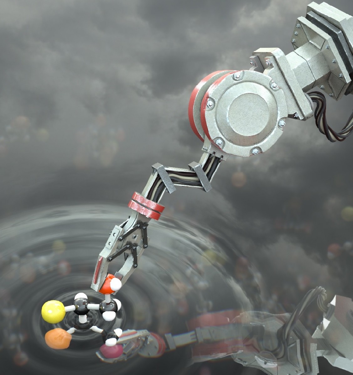
As a result, working with nanotechnology can have various payoffs, such as enhancing the performance of military products, said Patel. For instance, by manipulating nanomaterials, an engineer could make a weapon stronger, lighter, or increase its reactivity or durability.

“Generally, if you make something more safe, you make it less powerful,” said Stepanov. “But, with nanomaterials, you can make a product more safe and, in many cases, more powerful.”

There are two basic approaches to studying nanomaterials: bottom-up (building a large object atom by atom) and top-down (deconstructing a larger material.) Both approaches have been successfully employed in the development of nanoenergetics at ARDEC.

One of the challenges with manufacturing nonmaterials can be coping with shockwaves.

A shockwave initiates an explosive as it travels through a weapon’s main fill or the booster. When a shockwave travels through an energetic charge, it can hit small regions of defects, or voids, which heat up quickly and build pressure until the explosive reaches detonation. By using nanoenergetics, one could adjust the size and quantity of the defects and voids, so that the pressure isn’t as strong and ultimately prevent accidental detonation.

Nanomaterials also are difficult to process because they tend to agglomerate (stick together) and are also prone to Ostwald Ripening, or spontaneous growth of the crystals, which is especially pronounced at the nano-scale. This effect is commonly observed with ice cream, where ice can re-crystallize, resulting in a gritty texture.

“It’s a major production challenge because if you want to process nanomaterials–if you want to coat it with some polymer for explosives–any kind of medium that can dissolve these types of materials can promote ripening and you can end up with a product which no longer has the nanomaterial that you began with,” explained Stepanov.

However, nanotechnology research continues to grow at Picatinny as the research advances in the U.S. Army.

This ongoing development and future applicability encourages Patel and Stepanov to teach the nanomaterials and nanoenergetics course at Picatinny.

“I’m interested in making things better for the warfighter,” said Patel. “Nano-materials give you so many opportunities to do so. Also, as a scientist, it’s just a fascinating realm because you always get these little interesting surprises.

“You can know all the material science and equations, but then you get in the nano-world, and there’s something like a wrinkle–something you wouldn’t expect,” Patel added.

“It satisfies three deep needs: getting the warfighter technology, producing something of value, and it’s fun. You always see something new.”

Medieval church windows and the Lycurgus Cup

The shade of red in medieval church window glass is said to have been achieved by the use of gold nanoparticles. There is a source which claims the colour is due to copper rather than gold. I have not had to time to pursue the controversy such as it is but do have November 1, 2010 posting about stained glass and medieval churches which may prove of interest.

As for the Lycurgus Cup, it’s from the 4th century (CE or AD) and is an outstanding example of Roman art and craft. The glass in the cup is dichroic (it looks green or red depending on how the light catches it). The effect was achieved with the presence of gold and silver nanoparticles in the glass. I have a more extensive description and pictures in a Sept. 21, 2010 posting.

Final note

There is an  army initiative involving an educational institution, the Massachusetts Institute of Technology (MIT). The initiative is the MIT Institute for Soldier Nanotechnologies.