This venture into brain-like (neuromorphic) computing comes from France according to an August 17, 2021 news item on Nanowerk (Note: A link has been removed),
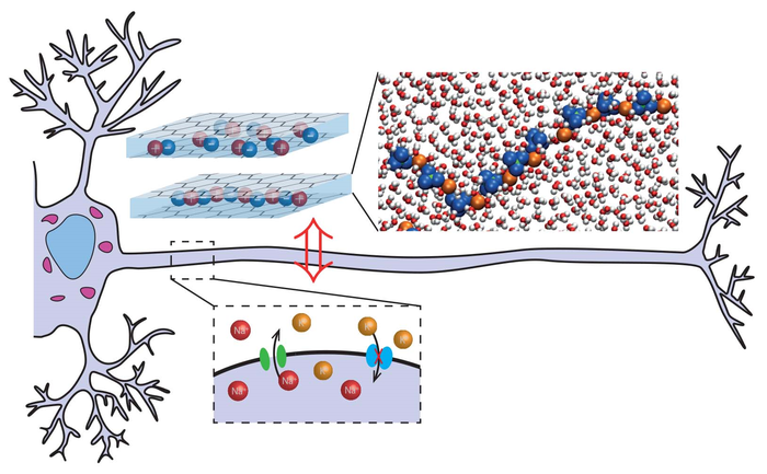
Brain-inspired electronics are the subject of intense research. Scientists from CNRS (Centre national de la recherche scientifique; French National Centre for Scientific Research) and the Ecole Normale Supérieure – PSL have theorized how to develop artificial neurons using, as nerve cells, ions to carry the information.
Their work, published in Science (“Modeling of emergent memory and voltage spiking in ionic transport through angstrom-scale slits”), reports that devices made of a single layer of water transporting ions within graphene nanoslits have the same transmission capacity as a neuron.
Au August 16, 2021 CNRS press release (also on EurekAlert but published August 6, 2021), which originated the news item, provides insight into the international interest in neuromorphic computing along with a few technical details about this latest research,
With an energy consumption equivalent to two bananas per day, the human brain can perform many complex tasks. Its high energy efficiency depends in particular on its base unit, the neuron, which has a membrane with nanometric pores called ion channels, which open and close according to the stimuli received. The resulting ion flows create an electric current responsible for the emission of action potentials, signals that allow neurons to communicate with each other.
Artificial intelligence can do all of these tasks but only at the cost of energy consumption tens of thousands of times that of the human brain. So the entire research challenge today is to design electronic systems that are as energy efficient as the human brain, for example, by using ions, not electrons, to carry the information. For this, nanofluidics, the study of how fluids behave in channels less than 100 nanometers wide, offer many perspectives. In a new study, a team from the ENS Laboratoire de Physique (CNRS/ENS-PSL/Sorbonne Université/Université de Paris) shows how to construct a prototype of an artificial neuron formed of extremely thin graphene slits containing a single layer of water molecules1. The scientists have shown that, under the effect of an electric field, the ions from this layer of water assemble into elongated clusters and develop a property known as the memristor effect: these clusters retain some of the stimuli that have been received in the past. To repeat the comparison with the brain, the graphene slits reproduce the ion channels, clusters and ion flows. And, using theoretical and digital tools, scientists have shown how to assemble these clusters to reproduce the physical mechanism of emission of action potentials, and thus the transmission of information.
This theoretical work continues experimentally within the French team, in collaboration with scientists from the University of Manchester (UK). The goal now is to prove experimentally that such systems can implement simple learning algorithms that can serve as the basis for tomorrow’s electronic memories.
1 Recently invented in Manchester by the group of André Geim (Nobel Prize in Physics 2010)
No brain but it learns, it has about 720 sexes, and it travels at a rate of approximately 4 cm (1.6 inches) per hour, it is known as ‘le blob’. Fascinated when I first stumbled across the news, I had to post this piece but wish I hadn’t waited so long.
A Paris zoo is showcasing a mysterious creature dubbed the “blob,” a yellowish collection of unicellular organisms called a slime mold that looks like a fungus, but acts like an animal.
This newest exhibit of the Paris Zoological Park, which goes on public display on Saturday [October 19, 2019], has no mouth, no stomach, no eyes, yet can detect food and digest it.
The blob also has almost 720 sexes, can move without legs or wings and heals itself in two minutes if cut in half.
…
The following video is in French but English subtitles are included,
Mike McRae offers more information in an October 17, 2019 article for Science Alert (Note: Links have been removed),
…
Here’s the 101: the 900-odd species of slime mould, of which P. polycephalum is just one, are a taxonomic headache. They’re currently boxed into the Protista kingdom, because where else are you going to put something that isn’t a fungus, plant, bacteria, or animal?
When life is good, they tend to live solitary lives as single cells like amoeba.
On occasion they squish together, forming a wide, branching structure called a plasmodium that can cover several square metres as they search cities to conquer. Well, bacteria to digest at least.
If you thought your experience on Tinder was hard, dating for slime moulds is a nightmare. Cells can only mix-and-match their genetic material if each has a compatible set of genes called matA, mat B, and mat C, each with up to 16 variations.
But the truly fascinating part is their ability to sense and rapidly adapt to their environment – a behaviour we might, for lack of a better word, call learning.
…
I have more about how ‘le blob’ learns. (All of this about learning and memory brings neuromorphic, sometimes called brain-like, computing to mind. My latest on that subject is a February 13, 2020 posting.) From a December 21, 2016 news item on ScienceDaily,
It isn’t an animal, a plant, or a fungus. The slime mold (Physarum polycephalum) is a strange, creeping, bloblike organism made up of one giant cell. Though it has no brain, it can learn from experience, as biologists at the Research Centre on Animal Cognition (CNRS, Université Toulouse III — Paul Sabatier) previously demonstrated. Now the same team of scientists has gone a step further, proving that a slime mold can transmit what it has learned to a fellow slime mold when the two combine. These new findings are published in the December 21, 2016, issue of the Proceedings of the Royal Society B.
Imagine you could temporarily fuse with someone, acquire that person’s knowledge, and then split off to become your separate self again. With slime molds, that really happens! The slime mold — Physarum polycephalum for scientists — is a unicellular organism whose natural habitat is forest litter. But it can also be cultured in a laboratory petri dish. Audrey Dussutour and David Vogel had already trained slime molds to move past repellent but harmless substances (e.g. coffee, quinine, or salt) to reach their food. They now reveal that a slime mold that has learned to ignore salt can transmit this acquired behavior to another simply by fusing with it.
To achieve this, the researchers taught more than 2,000 slime molds that salt posed no threat. In order to reach their food, these slime molds had to cross a bridge covered with salt. This experience made them habituated slime molds. Meanwhile, another 2,000 slime molds had to cross a bridge bare of any substance. They made up the group of naive slime molds. After this training period, the scientists grouped slime molds into habituated, naive, and mixed pairs. Paired slime molds fused together where they came into contact. The new, fused slime molds then had to cross salt-covered bridges. To the researchers’ surprise, the mixed slime molds moved just as fast as habituated pairs, and much faster than naive ones, suggesting that knowledge of the harmless nature of salt had been shared. This held true for slime molds formed from 3 or 4 individuals. No matter how many fused, only 1 habituated slime mold was needed to transfer the information.
To check that transfer had indeed taken place, the scientists separated the slime molds 1 hour and 3 hours after fusion and repeated the bridge experiment. Only naive slime molds that had been fused with habituated slime molds for 3 hours ignored the salt; all others were repulsed by it. This was proof of learning. When viewing the slime molds through a microscope, the scientists noticed that, after 3 hours, a vein formed at the point of fusion. This vein is undoubtedly the channel through which information is shared. The next challenges facing the researchers are to elucidate the form this information takes, and to test whether more than one behavior can be transmitted simultaneously. If Slime Mold A learns how to ignore quinine and Slime Mold B to ignore salt, the biologists wonder whether both behaviors can be transmitted and retained through fusion.
Here’s a link to and a citation for the paper published in 2016,
Le blob est un organisme unicellulaire complexe mais dépourvu de système nerveux. Celui-ci est capable d’emmagasiner une connaissance et de la transmettre à ses congénères mais la manière dont il procède demeurait un mystère. Des chercheuses et chercheurs du Centre de recherches sur la cognition animale (CNRS/UT3 Paul Sabatier)* viennent de montrer que le blob apprend à tolérer une substance en l’absorbant.
Cette découverte découle d’une observation : les blobs s’échangent de l’information seulement lorsque leurs réseaux veineux fusionnent. Dans ce cas-là, la connaissance circule-t-elle au travers de ces veines ? Dès lors, la substance à laquelle le blob s’habitue constitue-t-elle le support de sa « mémoire » ?
Dans un premier temps l’équipe de scientifiques a entrainé des blobs à traverser des environnements salés pendant six jours dans le but de les habituer au sel. Par la suite, elle a évalué la concentration en sel au sein de ces blobs : ceux-ci en contenaient dix fois plus que les blobs « naïfs ». Les chercheurs les ont alors placés dans un environnement neutre et ont observé qu’ils excrétaient le sel qu’ils contenaient au bout de deux jours, perdant de fait « la mémoire ». Cette expérience semblait donc indiquer un lien entre la concentration de sel au sein de l’organisme et la « mémoire » de l’apprentissage.
Pour aller plus loin et confirmer cette hypothèse, les scientifiques ont introduit dans des blobs naïfs la « mémoire » de l’habituation au sel en en injectant directement dans leurs organismes. Deux heures après, les blobs ne se comportaient plus comme des naïfs mais comme des blobs ayant subi un entrainement de six jours.
Lorsque les conditions environnementales se détériorent, les blobs sont capables d’entrer dans un état de dormance. Les chercheurs ont démontré qu’un mois après être entrés dans cet état, les blobs conservaient leur habituation au sel. Les blobs stockent en effet le sel absorbé pendant la phase de dormance et conservent ainsi la connaissance sur le long terme.
Les résultats de cette étude prouvent que la substance aversive pourrait constituer le support de la « mémoire » du blob. Les chercheurs essayent maintenant de comprendre si le blob peut mémoriser plusieurs substances aversives en même temps et dans quelle mesure il est capable de s’y habituer.
* Le Centre de recherche sur la cognition animale fait partie du Centre de biologie intégrative (CNRS/UT3 Paul Sabatier)
Here’s the abstract for the paper (the link and citation follow afterward),
Learning and memory are indisputably key features of animal success. Using information about past experiences is critical for optimal decision-making in a fluctuating environment. Those abilities are usually believed to be limited to organisms with a nervous system, precluding their existence in non-neural organisms. However, recent studies showed that the slime mould Physarum polycephalum, despite being unicellular, displays habituation, a simple form of learning. In this paper, we studied the possible substrate of both short- and long-term habituation in slime moulds. We habituated slime moulds to sodium, a known repellent, using a 6 day training and turned them into a dormant state named sclerotia. Those slime moulds were then revived and tested for habituation. We showed that information acquired during the training was preserved through the dormant stage as slime moulds still showed habituation after a one-month dormancy period. Chemical analyses indicated a continuous uptake of sodium during the process of habituation and showed that sodium was retained throughout the dormant stage. Lastly, we showed that memory inception via constrained absorption of sodium for 2 h elicited habituation. Our results suggest that slime moulds absorbed the repellent and used it as a ‘circulating memory’.
This article is part of the theme issue ‘Liquid brains, solid brains: How distributed cognitive architectures process information’.
Here’s the link and the citation for the 2019 paper,
Should you ever wish to find ‘le blob’, the Paris Zoological Park, known as the parc zoologique de Paris, is one of four establishments which comprise the totality of the Muséum national d’histoire naturelle in Paris. There are others outside Paris. (You can find more in the Muséum’s Wikipedia entry but it is in French.)
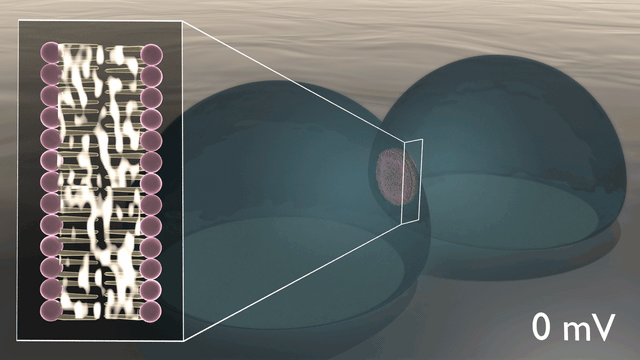
Caption: Researchers at ORNL’s Center for Nanophase Materials Sciences demonstrated the first example of capacitance in a lipid-based biomimetic membrane, opening nondigital routes to advanced, brain-like computation. Credit: Michelle Lehman/Oak Ridge National Laboratory, U.S. Dept. of Energy
The last time I wrote about memcapacitors (June 30, 2014 posting: Memristors, memcapacitors, and meminductors for faster computers), the ideas were largely theoretical; I believe this work is the first research I’ve seen on the topic. From an October 17, 2019 news item on ScienceDaily,
Researchers at the Department of Energy’s Oak Ridge National Laboratory ]ORNL], the University of Tennessee and Texas A&M University demonstrated bio-inspired devices that accelerate routes to neuromorphic, or brain-like, computing.
Results published in Nature Communications report the first example of a lipid-based “memcapacitor,” a charge storage component with memory that processes information much like synapses do in the brain. Their discovery could support the emergence of computing networks modeled on biology for a sensory approach to machine learning.
“Our goal is to develop materials and computing elements that work like biological synapses and neurons—with vast interconnectivity and flexibility—to enable autonomous systems that operate differently than current computing devices and offer new functionality and learning capabilities,” said Joseph Najem, a recent postdoctoral researcher at ORNL’s Center for Nanophase Materials Sciences, a DOE Office of Science User Facility, and current assistant professor of mechanical engineering at Penn State.
The novel approach uses soft materials to mimic biomembranes and simulate the way nerve cells communicate with one another.
The team designed an artificial cell membrane, formed at the interface of two lipid-coated water droplets in oil, to explore the material’s dynamic, electrophysiological properties. At applied voltages, charges build up on both sides of the membrane as stored energy, analogous to the way capacitors work in traditional electric circuits.
But unlike regular capacitors, the memcapacitor can “remember” a previously applied voltage and—literally—shape how information is processed. The synthetic membranes change surface area and thickness depending on electrical activity. These shapeshifting membranes could be tuned as adaptive filters for specific biophysical and biochemical signals.
“The novel functionality opens avenues for nondigital signal processing and machine learning modeled on nature,” said ORNL’s Pat Collier, a CNMS staff research scientist.
A distinct feature of all digital computers is the separation of processing and memory. Information is transferred back and forth from the hard drive and the central processor, creating an inherent bottleneck in the architecture no matter how small or fast the hardware can be.
Neuromorphic computing, modeled on the nervous system, employs architectures that are fundamentally different in that memory and signal processing are co-located in memory elements—memristors, memcapacitors and meminductors.
These “memelements” make up the synaptic hardware of systems that mimic natural information processing, learning and memory.
Systems designed with memelements offer advantages in scalability and low power consumption, but the real goal is to carve out an alternative path to artificial intelligence, said Collier.
Tapping into biology could enable new computing possibilities, especially in the area of “edge computing,” such as wearable and embedded technologies that are not connected to a cloud but instead make on-the-fly decisions based on sensory input and past experience.
Biological sensing has evolved over billions of years into a highly sensitive system with receptors in cell membranes that are able to pick out a single molecule of a specific odor or taste. “This is not something we can match digitally,” Collier said.
Digital computation is built around digital information, the binary language of ones and zeros coursing through electronic circuits. It can emulate the human brain, but its solid-state components do not compute sensory data the way a brain does.
“The brain computes sensory information pushed through synapses in a neural network that is reconfigurable and shaped by learning,” said Collier. “Incorporating biology—using biomembranes that sense bioelectrochemical information—is key to developing the functionality of neuromorphic computing.”
While numerous solid-state versions of memelements have been demonstrated, the team’s biomimetic elements represent new opportunities for potential “spiking” neural networks that can compute natural data in natural ways.
Spiking neural networks are intended to simulate the way neurons spike with electrical potential and, if the signal is strong enough, pass it on to their neighbors through synapses, carving out learning pathways that are pruned over time for efficiency.
A bio-inspired version with analog data processing is a distant aim. Current early-stage research focuses on developing the components of bio-circuitry.
“We started with the basics, a memristor that can weigh information via conductance to determine if a spike is strong enough to be broadcast through a network of synapses connecting neurons,” said Collier. “Our memcapacitor goes further in that it can actually store energy as an electric charge in the membrane, enabling the complex ‘integrate and fire’ activity of neurons needed to achieve dense networks capable of brain-like computation.”
The team’s next steps are to explore new biomaterials and study simple networks to achieve more complex brain-like functionalities with memelements.
Here’s a link to and a citation for the paper,
Dynamical nonlinear memory capacitance in biomimetic membranes by Joseph S. Najem, Md Sakib Hasan, R. Stanley Williams, Ryan J. Weiss, Garrett S. Rose, Graham J. Taylor, Stephen A. Sarles & C. Patrick Collier. Nature Communications volume 10, Article number: 3239 (2019) DOI: DOIhttps://doi.org/10.1038/s41467-019-11223-8 Published July 19, 2019
This paper is open access.
One final comment, you might recognize one of the authors (R. Stanley Williams) who in 2008 helped launch ‘memristor’ research.
It seems the US National Institute of Standards and Technology (NIST) is more deeply invested into developing artificial brains than I had realized (See: April 17, 2018 posting). A January 26, 2018 NIST news release on EurekAlert describes the organization’s latest foray into the field,
Researchers at the National Institute of Standards and Technology (NIST) have built a superconducting switch that “learns” like a biological system and could connect processors and store memories in future computers operating like the human brain.
The NIST switch, described in Science Advances, is called a synapse, like its biological counterpart, and it supplies a missing piece for so-called neuromorphic computers. Envisioned as a new type of artificial intelligence, such computers could boost perception and decision-making for applications such as self-driving cars and cancer diagnosis.
A synapse is a connection or switch between two brain cells. NIST’s artificial synapse–a squat metallic cylinder 10 micrometers in diameter–is like the real thing because it can process incoming electrical spikes to customize spiking output signals. This processing is based on a flexible internal design that can be tuned by experience or its environment. The more firing between cells or processors, the stronger the connection. Both the real and artificial synapses can thus maintain old circuits and create new ones. Even better than the real thing, the NIST synapse can fire much faster than the human brain–1 billion times per second, compared to a brain cell’s 50 times per second–using just a whiff of energy, about one ten-thousandth as much as a human synapse. In technical terms, the spiking energy is less than 1 attojoule, lower than the background energy at room temperature and on a par with the chemical energy bonding two atoms in a molecule.
“The NIST synapse has lower energy needs than the human synapse, and we don’t know of any other artificial synapse that uses less energy,” NIST physicist Mike Schneider said.
The new synapse would be used in neuromorphic computers made of superconducting components, which can transmit electricity without resistance, and therefore, would be more efficient than other designs based on semiconductors or software. Data would be transmitted, processed and stored in units of magnetic flux. Superconducting devices mimicking brain cells and transmission lines have been developed, but until now, efficient synapses–a crucial piece–have been missing.
The brain is especially powerful for tasks like context recognition because it processes data both in sequence and simultaneously and stores memories in synapses all over the system. A conventional computer processes data only in sequence and stores memory in a separate unit.
The NIST synapse is a Josephson junction, long used in NIST voltage standards. These junctions are a sandwich of superconducting materials with an insulator as a filling. When an electrical current through the junction exceeds a level called the critical current, voltage spikes are produced. The synapse uses standard niobium electrodes but has a unique filling made of nanoscale clusters of manganese in a silicon matrix.
The nanoclusters–about 20,000 per square micrometer–act like tiny bar magnets with “spins” that can be oriented either randomly or in a coordinated manner.
“These are customized Josephson junctions,” Schneider said. “We can control the number of nanoclusters pointing in the same direction, which affects the superconducting properties of the junction.”
The synapse rests in a superconducting state, except when it’s activated by incoming current and starts producing voltage spikes. Researchers apply current pulses in a magnetic field to boost the magnetic ordering, that is, the number of nanoclusters pointing in the same direction. This magnetic effect progressively reduces the critical current level, making it easier to create a normal conductor and produce voltage spikes.
The critical current is the lowest when all the nanoclusters are aligned. The process is also reversible: Pulses are applied without a magnetic field to reduce the magnetic ordering and raise the critical current. This design, in which different inputs alter the spin alignment and resulting output signals, is similar to how the brain operates.
Synapse behavior can also be tuned by changing how the device is made and its operating temperature. By making the nanoclusters smaller, researchers can reduce the pulse energy needed to raise or lower the magnetic order of the device. Raising the operating temperature slightly from minus 271.15 degrees C (minus 456.07 degrees F) to minus 269.15 degrees C (minus 452.47 degrees F), for example, results in more and higher voltage spikes.
Crucially, the synapses can be stacked in three dimensions (3-D) to make large systems that could be used for computing. NIST researchers created a circuit model to simulate how such a system would operate.
The NIST synapse’s combination of small size, superfast spiking signals, low energy needs and 3-D stacking capability could provide the means for a far more complex neuromorphic system than has been demonstrated with other technologies, according to the paper.
NIST has prepared an animation illustrating the research,
Caption: This is an animation of how NIST’s artificial synapse works. Credit: Sean Kelley/NIST
Here’s a link to and a citation for the paper,
Ultralow power artificial synapses using nanotextured magnetic Josephson junctions by Michael L. Schneider, Christine A. Donnelly, Stephen E. Russek, Burm Baek, Matthew R. Pufall, Peter F. Hopkins, Paul D. Dresselhaus, Samuel P. Benz, and William H. Rippard. Science Advances 26 Jan 2018: Vol. 4, no. 1, e1701329 DOI: 10.1126/sciadv.1701329
This paper is open access.
Samuel K. Moore in a January 26, 2018 posting on the Nanoclast blog (on the IEEE [Institute for Electrical and Electronics Engineers] website) describes the research and adds a few technical explanations such as this about the Josephson junction,
In a magnetic Josephson junction, that “weak link” is magnetic. The higher the magnetic field, the lower the critical current needed to produce voltage spikes. In the device Schneider and his colleagues designed, the magnetic field is caused by 20,000 or so nanometer-scale clusters of manganese embedded in silicon. …
Moore also provides some additional links including this one to his November 29, 2017 posting where he describes four new approaches to computing including quantum computing and neuromorphic (brain-like) computing.
I first stumbled onto memristors and the possibility of brain-like computing sometime in 2008 (around the time that R. Stanley Williams and his team at HP Labs first published the results of their research linking Dr. Leon Chua’s memristor theory to their attempts to shrink computer chips). In the almost 10 years since, scientists have worked hard to utilize memristors in the field of neuromorphic (brain-like) engineering/computing.
When it comes to processing power, the human brain just can’t be beat.
Packed within the squishy, football-sized organ are somewhere around 100 billion neurons. At any given moment, a single neuron can relay instructions to thousands of other neurons via synapses—the spaces between neurons, across which neurotransmitters are exchanged. There are more than 100 trillion synapses that mediate neuron signaling in the brain, strengthening some connections while pruning others, in a process that enables the brain to recognize patterns, remember facts, and carry out other learning tasks, at lightning speeds.
Researchers in the emerging field of “neuromorphic computing” have attempted to design computer chips that work like the human brain. Instead of carrying out computations based on binary, on/off signaling, like digital chips do today, the elements of a “brain on a chip” would work in an analog fashion, exchanging a gradient of signals, or “weights,” much like neurons that activate in various ways depending on the type and number of ions that flow across a synapse.
In this way, small neuromorphic chips could, like the brain, efficiently process millions of streams of parallel computations that are currently only possible with large banks of supercomputers. But one significant hangup on the way to such portable artificial intelligence has been the neural synapse, which has been particularly tricky to reproduce in hardware.
Now engineers at MIT [Massachusetts Institute of Technology] have designed an artificial synapse in such a way that they can precisely control the strength of an electric current flowing across it, similar to the way ions flow between neurons. The team has built a small chip with artificial synapses, made from silicon germanium. In simulations, the researchers found that the chip and its synapses could be used to recognize samples of handwriting, with 95 percent accuracy.
The design, published today [January 22, 2018] in the journal Nature Materials, is a major step toward building portable, low-power neuromorphic chips for use in pattern recognition and other learning tasks.
The research was led by Jeehwan Kim, the Class of 1947 Career Development Assistant Professor in the departments of Mechanical Engineering and Materials Science and Engineering, and a principal investigator in MIT’s Research Laboratory of Electronics and Microsystems Technology Laboratories. His co-authors are Shinhyun Choi (first author), Scott Tan (co-first author), Zefan Li, Yunjo Kim, Chanyeol Choi, and Hanwool Yeon of MIT, along with Pai-Yu Chen and Shimeng Yu of Arizona State University.
Too many paths
Most neuromorphic chip designs attempt to emulate the synaptic connection between neurons using two conductive layers separated by a “switching medium,” or synapse-like space. When a voltage is applied, ions should move in the switching medium to create conductive filaments, similarly to how the “weight” of a synapse changes.
But it’s been difficult to control the flow of ions in existing designs. Kim says that’s because most switching mediums, made of amorphous materials, have unlimited possible paths through which ions can travel — a bit like Pachinko, a mechanical arcade game that funnels small steel balls down through a series of pins and levers, which act to either divert or direct the balls out of the machine.
Like Pachinko, existing switching mediums contain multiple paths that make it difficult to predict where ions will make it through. Kim says that can create unwanted nonuniformity in a synapse’s performance.
“Once you apply some voltage to represent some data with your artificial neuron, you have to erase and be able to write it again in the exact same way,” Kim says. “But in an amorphous solid, when you write again, the ions go in different directions because there are lots of defects. This stream is changing, and it’s hard to control. That’s the biggest problem — nonuniformity of the artificial synapse.”
A perfect mismatch
Instead of using amorphous materials as an artificial synapse, Kim and his colleagues looked to single-crystalline silicon, a defect-free conducting material made from atoms arranged in a continuously ordered alignment. The team sought to create a precise, one-dimensional line defect, or dislocation, through the silicon, through which ions could predictably flow.
To do so, the researchers started with a wafer of silicon, resembling, at microscopic resolution, a chicken-wire pattern. They then grew a similar pattern of silicon germanium — a material also used commonly in transistors — on top of the silicon wafer. Silicon germanium’s lattice is slightly larger than that of silicon, and Kim found that together, the two perfectly mismatched materials can form a funnel-like dislocation, creating a single path through which ions can flow.
The researchers fabricated a neuromorphic chip consisting of artificial synapses made from silicon germanium, each synapse measuring about 25 nanometers across. They applied voltage to each synapse and found that all synapses exhibited more or less the same current, or flow of ions, with about a 4 percent variation between synapses — a much more uniform performance compared with synapses made from amorphous material.
They also tested a single synapse over multiple trials, applying the same voltage over 700 cycles, and found the synapse exhibited the same current, with just 1 percent variation from cycle to cycle.
“This is the most uniform device we could achieve, which is the key to demonstrating artificial neural networks,” Kim says.
Writing, recognized
As a final test, Kim’s team explored how its device would perform if it were to carry out actual learning tasks — specifically, recognizing samples of handwriting, which researchers consider to be a first practical test for neuromorphic chips. Such chips would consist of “input/hidden/output neurons,” each connected to other “neurons” via filament-based artificial synapses.
Scientists believe such stacks of neural nets can be made to “learn.” For instance, when fed an input that is a handwritten ‘1,’ with an output that labels it as ‘1,’ certain output neurons will be activated by input neurons and weights from an artificial synapse. When more examples of handwritten ‘1s’ are fed into the same chip, the same output neurons may be activated when they sense similar features between different samples of the same letter, thus “learning” in a fashion similar to what the brain does.
Kim and his colleagues ran a computer simulation of an artificial neural network consisting of three sheets of neural layers connected via two layers of artificial synapses, the properties of which they based on measurements from their actual neuromorphic chip. They fed into their simulation tens of thousands of samples from a handwritten recognition dataset commonly used by neuromorphic designers, and found that their neural network hardware recognized handwritten samples 95 percent of the time, compared to the 97 percent accuracy of existing software algorithms.
The team is in the process of fabricating a working neuromorphic chip that can carry out handwriting-recognition tasks, not in simulation but in reality. Looking beyond handwriting, Kim says the team’s artificial synapse design will enable much smaller, portable neural network devices that can perform complex computations that currently are only possible with large supercomputers.
“Ultimately we want a chip as big as a fingernail to replace one big supercomputer,” Kim says. “This opens a stepping stone to produce real artificial hardware.”
This research was supported in part by the National Science Foundation.
In January 2018 it seemed like I was tripping across a lot of memristor stories . This came from a January 19, 2018 news item on Nanowerk,
In the race to build a computer that mimics the massive computational power of the human brain, researchers are increasingly turning to memristors, which can vary their electrical resistance based on the memory of past activity. Scientists at the National Institute of Standards and Technology (NIST) have now unveiled the long-mysterious inner workings of these semiconductor elements, which can act like the short-term memory of nerve cells.
Just as the ability of one nerve cell to signal another depends on how often the cells have communicated in the recent past, the resistance of a memristor depends on the amount of current that recently flowed through it. Moreover, a memristor retains that memory even when electrical power is switched off.
But despite the keen interest in memristors, scientists have lacked a detailed understanding of how these devices work and have yet to develop a standard toolset to study them.
Now, NIST scientists have identified such a toolset and used it to more deeply probe how memristors operate. Their findings could lead to more efficient operation of the devices and suggest ways to minimize the leakage of current.
Brian Hoskins of NIST and the University of California, Santa Barbara, along with NIST scientists Nikolai Zhitenev, Andrei Kolmakov, Jabez McClelland and their colleagues from the University of Maryland’s NanoCenter (link is external) in College Park and the Institute for Research and Development in Microtechnologies in Bucharest, reported the findings (link is external) in a recent Nature Communications.
To explore the electrical function of memristors, the team aimed a tightly focused beam of electrons at different locations on a titanium dioxide memristor. The beam knocked free some of the device’s electrons, which formed ultrasharp images of those locations. The beam also induced four distinct currents to flow within the device. The team determined that the currents are associated with the multiple interfaces between materials in the memristor, which consists of two metal (conducting) layers separated by an insulator.
“We know exactly where each of the currents are coming from because we are controlling the location of the beam that is inducing those currents,” said Hoskins.
In imaging the device, the team found several dark spots—regions of enhanced conductivity—which indicated places where current might leak out of the memristor during its normal operation. These leakage pathways resided outside the memristor’s core—where it switches between the low and high resistance levels that are useful in an electronic device. The finding suggests that reducing the size of a memristor could minimize or even eliminate some of the unwanted current pathways. Although researchers had suspected that might be the case, they had lacked experimental guidance about just how much to reduce the size of the device.
Because the leakage pathways are tiny, involving distances of only 100 to 300 nanometers, “you’re probably not going to start seeing some really big improvements until you reduce dimensions of the memristor on that scale,” Hoskins said.
To their surprise, the team also found that the current that correlated with the memristor’s switch in resistance didn’t come from the active switching material at all, but the metal layer above it. The most important lesson of the memristor study, Hoskins noted, “is that you can’t just worry about the resistive switch, the switching spot itself, you have to worry about everything around it.” The team’s study, he added, “is a way of generating much stronger intuition about what might be a good way to engineer memristors.”
It might be my imagination but it seemed like a lot of papers from 2017 were being publicized in early 2018.
Finally, I borrowed much of my headline from the NIST’s headline for its news release, specifically, “Thanks for the memory,” which is a rather old song,
Bob Hope and Shirley Ross in “The Big Broadcast of 1938.”
This new ‘breed’ of memristor (a component in brain-like/neuromorphic computing) is a kind of thin film. First, here’s an explanation of neuromorphic computing from the Finnish researchers looking into a new kind of memristor, from a January 10, 2018 news item on Nanowerk,
The internet of things [IOT] is coming, that much we know. But still it won’t; not until we have components and chips that can handle the explosion of data that comes with IoT. In 2020, there will already be 50 billion industrial internet sensors in place all around us. A single autonomous device – a smart watch, a cleaning robot, or a driverless car – can produce gigabytes of data each day, whereas an airbus may have over 10 000 sensors in one wing alone.
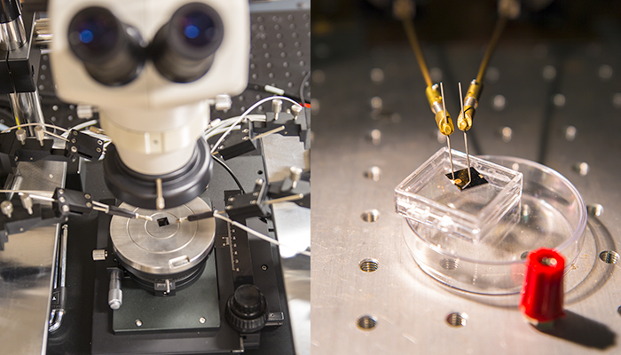
Two hurdles need to be overcome. First, current transistors in computer chips must be miniaturized to the size of only few nanometres; the problem is they won’t work anymore then. Second, analysing and storing unprecedented amounts of data will require equally huge amounts of energy. Sayani Majumdar, Academy Fellow at Aalto University, along with her colleagues, is designing technology to tackle both issues.
Majumdar has with her colleagues designed and fabricated the basic building blocks of future components in what are called “neuromorphic” computers inspired by the human brain. It’s a field of research on which the largest ICT companies in the world and also the EU are investing heavily. Still, no one has yet come up with a nano-scale hardware architecture that could be scaled to industrial manufacture and use.
“The technology and design of neuromorphic computing is advancing more rapidly than its rival revolution, quantum computing. There is already wide speculation both in academia and company R&D about ways to inscribe heavy computing capabilities in the hardware of smart phones, tablets and laptops. The key is to achieve the extreme energy-efficiency of a biological brain and mimic the way neural networks process information through electric impulses,” explains Majumdar.
Basic components for computers that work like the brain
In their recent article in Advanced Functional Materials, Majumdar and her team show how they have fabricated a new breed of “ferroelectric tunnel junctions”, that is, few-nanometre-thick ferroelectric thin films sandwiched between two electrodes. They have abilities beyond existing technologies and bode well for energy-efficient and stable neuromorphic computing.
The junctions work in low voltages of less than five volts and with a variety of electrode materials – including silicon used in chips in most of our electronics. They also can retain data for more than 10 years without power and be manufactured in normal conditions.
Tunnel junctions have up to this point mostly been made of metal oxides and require 700 degree Celsius temperatures and high vacuums to manufacture. Ferroelectric materials also contain lead which makes them – and all our computers – a serious environmental hazard.
“Our junctions are made out of organic hydro-carbon materials and they would reduce the amount of toxic heavy metal waste in electronics. We can also make thousands of junctions a day in room temperature without them suffering from the water or oxygen in the air”, explains Majumdar.
What makes ferroelectric thin film components great for neuromorphic computers is their ability to switch between not only binary states – 0 and 1 – but a large number of intermediate states as well. This allows them to ‘memorise’ information not unlike the brain: to store it for a long time with minute amounts of energy and to retain the information they have once received – even after being switched off and on again.
We are no longer talking of transistors, but ‘memristors’. They are ideal for computation similar to that in biological brains. Take for example the Mars 2020 Rover about to go chart the composition of another planet. For the Rover to work and process data on its own using only a single solar panel as an energy source, the unsupervised algorithms in it will need to use an artificial brain in the hardware.
“What we are striving for now, is to integrate millions of our tunnel junction memristors into a network on a one square centimetre area. We can expect to pack so many in such a small space because we have now achieved a record-high difference in the current between on and off-states in the junctions and that provides functional stability. The memristors could then perform complex tasks like image and pattern recognition and make decisions autonomously,” says Majumdar.
The probe-station device (the full instrument, left, and a closer view of the device connection, right) which measures the electrical responses of the basic components for computers mimicking the human brain. The tunnel junctions are on a thin film on the substrate plate. Photo: Tapio Reinekoski
In trying to bring brain-like (neuromorphic) computing closer to reality, researchers have been working on the development of memory resistors, or memristors, which are resistors in a circuit that ‘remember’ their state even if you lose power.
Today, most computers use random access memory (RAM), which moves very quickly as a user works but does not retain unsaved data if power is lost. Flash drives, on the other hand, store information when they are not powered but work much slower. Memristors could provide a memory that is the best of both worlds: fast and reliable.
He goes on to discuss a team at the University of Texas at Austin’s work on creating an extraordinarily thin memristor: an atomristor,
he team’s work features the thinnest memory devices and it appears to be a universal effect available in all semiconducting 2D monolayers.
The scientists explain that the unexpected discovery of nonvolatile resistance switching (NVRS) in monolayer transitional metal dichalcogenides (MoS2, MoSe2, WS2, WSe2) is likely due to the inherent layered crystalline nature that produces sharp interfaces and clean tunnel barriers. This prevents excessive leakage and affords stable phenomenon so that NVRS can be used for existing memory and computing applications.
“Our work opens up a new field of research in exploiting defects at the atomic scale, and can advance existing applications such as future generation high density storage, and 3D cross-bar networks for neuromorphic memory computing,” notes Akinwande [Deji Akinwande, an Associate Professor at the University of Texas at Austin]. “We also discovered a completely new application, which is non-volatile switching for radio-frequency (RF) communication systems. This is a rapidly emerging field because of the massive growth in wireless technologies and the need for very low-power switches. Our devices consume no static power, an important feature for battery life in mobile communication systems.”
…
Here’s a link to and a citation for the Akinwande team’s paper,
ETA January 23, 2018: There’s another account of the atomristor in Samuel K. Moore’s January 23, 2018 posting on the Nanoclast blog (on the IEEE [Institute of Electrical and Electronics Engineers] website).
As you might suspect, a neuristor is based on a memristor .(For a description of a memristor there’s this Wikipedia entry and you can search this blog with the tags ‘memristor’ and neuromorphic engineering’ for more here.)
Being new to neuristors ,I needed a little more information before reading the latest and found this Dec. 24, 2012 article by John Timmer for Ars Technica (Note: Links have been removed),
Computing hardware is composed of a series of binary switches; they’re either on or off. The other piece of computational hardware we’re familiar with, the brain, doesn’t work anything like that. Rather than being on or off, individual neurons exhibit brief spikes of activity, and encode information in the pattern and timing of these spikes. The differences between the two have made it difficult to model neurons using computer hardware. In fact, the recent, successful generation of a flexible neural system required that each neuron be modeled separately in software in order to get the sort of spiking behavior real neurons display.
But researchers may have figured out a way to create a chip that spikes. The people at HP labs who have been working on memristors have figured out a combination of memristors and capacitors that can create a spiking output pattern. Although these spikes appear to be more regular than the ones produced by actual neurons, it might be possible to create versions that are a bit more variable than this one. And, more significantly, it should be possible to fabricate them in large numbers, possibly right on a silicon chip.
The key to making the devices is something called a Mott insulator. These are materials that would normally be able to conduct electricity, but are unable to because of interactions among their electrons. Critically, these interactions weaken with elevated temperatures. So, by heating a Mott insulator, it’s possible to turn it into a conductor. In the case of the material used here, NbO2, the heat is supplied by resistance itself. By applying a voltage to the NbO2 in the device, it becomes a resistor, heats up, and, when it reaches a critical temperature, turns into a conductor, allowing current to flow through. But, given the chance to cool off, the device will return to its resistive state. Formally, this behavior is described as a memristor.
To get the sort of spiking behavior seen in a neuron, the authors turned to a simplified model of neurons based on the proteins that allow them to transmit electrical signals. When a neuron fires, sodium channels open, allowing ions to rush into a nerve cell, and changing the relative charges inside and outside its membrane. In response to these changes, potassium channels then open, allowing different ions out, and restoring the charge balance. That shuts the whole thing down, and allows various pumps to start restoring the initial ion balance.
…
Here’s a link to and a citation for the research paper described in Timmer’s article,
A scalable neuristor built with Mott memristors by Matthew D. Pickett, Gilberto Medeiros-Ribeiro, & R. Stanley Williams. Nature Materials 12, 114–117 (2013) doi:10.1038/nmat3510 Published online 16 December 2012
A future android brain like that of Star Trek’s Commander Data might contain neuristors, multi-circuit components that emulate the firings of human neurons.
Neuristors already exist today in labs, in small quantities, and to fuel the quest to boost neuristors’ power and numbers for practical use in brain-like computing, the U.S. Department of Defense has awarded a $7.1 million grant to a research team led by the Georgia Institute of Technology. The researchers will mainly work on new metal oxide materials that buzz electronically at the nanoscale to emulate the way human neural networks buzz with electric potential on a cellular level.
A July 28, 2017 Georgia Tech news release, which originated the news item, delves further into neuristors and the proposed work leading to an artificial retina that can learn (!). This was not where I was expecting things to go,
But let’s walk expectations back from the distant sci-fi future into the scientific present: The research team is developing its neuristor materials to build an intelligent light sensor, and not some artificial version of the human brain, which would require hundreds of trillions of circuits.
But an artificial retina that can learn autonomously appears well within reach of the research team from Georgia Tech and Binghamton University. Despite the term “retina,” the development is not intended as a medical implant, but it could be used in advanced image recognition cameras for national defense and police work.
At the same time, it would significantly advance brain-mimicking, or neuromorphic, computing. The research field that takes its cues from what science already does know about how the brain computes to develop exponentially more powerful computing.
The retina would be comprised of an array of ultra-compact circuits called neuristors (a word combining “neuron” and “transistor”) that sense light, compute an image out of it and store the image. All three of the functions would occur simultaneously and nearly instantaneously.
“The same device senses, computes and stores the image,” Doolittle said. “The device is the sensor, and it’s the processor, and it’s the memory all at the same time.” A neuristor itself is comprised in part of devices called memristors inspired by the way human neurons work.
Brain vs. PC
That cuts out loads of processing and memory lag time that are inherent in traditional computing.
Take the device you’re reading this article on: Its microprocessor has to tap a separate memory component to get data, then do some processing, tap memory again for more data, process some more, etc. “That back-and-forth from memory to microprocessor has created a bottleneck,” Doolittle said.
A neuristor array breaks the bottleneck by emulating the extreme flexibility of biological nervous systems: When a brain computes, it uses a broad set of neural pathways that flash with enormous data. Then, later, to compute the same thing again, it will use quite different neural paths.
Traditional computer pathways, by contrast, are hardwired. For example, look at a present-day processor and you’ll see lines etched into it. Those are pathways that computational signals are limited to.
The new memristor materials at the heart of the neuristor are not etched, and signals flow through the surface very freely, more like they do through the brain, exponentially increasing the number of possible pathways computation can take. That helps the new intelligent retina compute powerfully and swiftly.
Terrorists, missing children
The retina’s memory could also store thousands of photos, allowing it to immediately match up what it sees with the saved images. The retina could pinpoint known terror suspects in a crowd, find missing children, or identify enemy aircraft virtually instantaneously, without having to trawl databases to correctly identify what is in the images.
Even if you take away the optics, the new neuristor arrays still advance artificial intelligence. Instead of light, a surface of neuristors could absorb massive data streams at once, compute them, store them, and compare them to patterns of other data, immediately. It could even autonomously learn to extrapolate further information, like calculating the third dimension out of data from two dimensions.
“It will work with anything that has a repetitive pattern like radar signatures, for example,” Doolittle said. “Right now, that’s too challenging to compute, because radar information is flying out at such a high data rate that no computer can even think about keeping up.”
Smart materials
The research project’s title acronym CEREBRAL may hint at distant dreams of an artificial brain, but what it stands for spells out the present goal in neuromorphic computing: Cross-disciplinary Electronic-ionic Research Enabling Biologically Realistic Autonomous Learning.
The new materials have already been created, and they work, but the researchers don’t yet fully understand why.
Much of the project is dedicated to examining quantum states in the materials and how those states help create useful electronic-ionic properties. Researchers will view them by bombarding the metal oxides with extremely bright x-ray photons at the recently constructed National Synchrotron Light Source II.
Grant sub-awardee Binghamton University is located close by, and Binghamton physicists will run experiments and hone them via theoretical modeling.
‘Sea of lithium’
The neuristors are created mainly by the way the metal oxide materials are grown in the lab, which has advantages over building neuristors in a more wired way.
This materials-growing approach is conducive to mass production. Also, though neuristors in general free signals to take multiple pathways, Georgia Tech’s neuristors do it much more flexibly thanks to chemical properties.
“We also have a sea of lithium, and it’s like an infinite reservoir of computational ionic fluid,” Doolittle said. The lithium niobite imitates the way ionic fluid bathes biological neurons and allows them to flash with electric potential while signaling. In a neuristor array, the lithium niobite helps computational signaling move in myriad directions.
“It’s not like the typical semiconductor material, where you etch a line, and only that line has the computational material,” Doolittle said.
Commander Data’s brain?
“Unlike any other previous neuristors, our neuristors will adapt themselves in their computational-electronic pulsing on the fly, which makes them more like a neurological system,” Doolittle said. “They mimic biology in that we have ion drift across the material to create the memristors (the memory part of neuristors).”
Brains are far superior to computers at most things, but not all. Brains recognize objects and do motor tasks much better. But computers are much better at arithmetic and data processing.
Neuristor arrays can meld both types of computing, making them biological and algorithmic at once, a bit like Commander Data’s brain.
…
The research is being funded through the U.S. Department of Defense’s Multidisciplinary University Research Initiatives (MURI) Program under grant number FOA: N00014-16-R-FO05. Any opinions, findings, and conclusions or recommendations expressed in this material are those of the authors and do not necessarily reflect the views of those agencies.
Researchers are always searching for improved technologies, but the most efficient computer possible already exists. It can learn and adapt without needing to be programmed or updated. It has nearly limitless memory, is difficult to crash, and works at extremely fast speeds. It’s not a Mac or a PC; it’s the human brain. And scientists around the world want to mimic its abilities.
Both academic and industrial laboratories are working to develop computers that operate more like the human brain. Instead of operating like a conventional, digital system, these new devices could potentially function more like a network of neurons.
“Computers are very impressive in many ways, but they’re not equal to the mind,” said Mark Hersam, the Bette and Neison Harris Chair in Teaching Excellence in Northwestern University’s McCormick School of Engineering. “Neurons can achieve very complicated computation with very low power consumption compared to a digital computer.”
A team of Northwestern researchers, including Hersam, has accomplished a new step forward in electronics that could bring brain-like computing closer to reality. The team’s work advances memory resistors, or “memristors,” which are resistors in a circuit that “remember” how much current has flowed through them.
…
“Memristors could be used as a memory element in an integrated circuit or computer,” Hersam said. “Unlike other memories that exist today in modern electronics, memristors are stable and remember their state even if you lose power.”
Current computers use random access memory (RAM), which moves very quickly as a user works but does not retain unsaved data if power is lost. Flash drives, on the other hand, store information when they are not powered but work much slower. Memristors could provide a memory that is the best of both worlds: fast and reliable. But there’s a problem: memristors are two-terminal electronic devices, which can only control one voltage channel. Hersam wanted to transform it into a three-terminal device, allowing it to be used in more complex electronic circuits and systems.
The memristor is of some interest to a number of other parties prominent amongst them, the University of Michigan’s Professor Wei Lu and HP (Hewlett Packard) Labs, both of whom are mentioned in one of my more recent memristor pieces, a June 26, 2014 post.
Getting back to Northwestern,
Hersam and his team met this challenge by using single-layer molybdenum disulfide (MoS2), an atomically thin, two-dimensional nanomaterial semiconductor. Much like the way fibers are arranged in wood, atoms are arranged in a certain direction–called “grains”–within a material. The sheet of MoS2 that Hersam used has a well-defined grain boundary, which is the interface where two different grains come together.
“Because the atoms are not in the same orientation, there are unsatisfied chemical bonds at that interface,” Hersam explained. “These grain boundaries influence the flow of current, so they can serve as a means of tuning resistance.”
When a large electric field is applied, the grain boundary literally moves, causing a change in resistance. By using MoS2 with this grain boundary defect instead of the typical metal-oxide-metal memristor structure, the team presented a novel three-terminal memristive device that is widely tunable with a gate electrode.
“With a memristor that can be tuned with a third electrode, we have the possibility to realize a function you could not previously achieve,” Hersam said. “A three-terminal memristor has been proposed as a means of realizing brain-like computing. We are now actively exploring this possibility in the laboratory.”
This paper is behind a paywall but there is a few preview available through ReadCube Access.
Dexter Johnson has written about this latest memristor development in an April 9, 2015 posting on his Nanoclast blog (on the IEEE [Institute for Electrical and Electronics Engineers] website) where he notes this (Note: A link has been removed),
The memristor seems to generate fairly polarized debate, especially here on this website in the comments on stories covering the technology. The controversy seems to fall along the lines that the device that HP Labs’ Stan Williams and Greg Snider developed back in 2008 doesn’t exactly line up with the original theory of the memristor proposed by Leon Chua back in 1971.
It seems the ‘debate’ has evolved from issues about how the memristor is categorized. I wonder if there’s still discussion about whether or not HP Labs is attempting to develop a patent thicket of sorts.