Tag Archives: Brookhaven National Laboratory (BNL)

Chatbot with expertise in nanomaterials

This December 1, 2023 news item on phys.org starts with a story,

A researcher has just finished writing a scientific paper. She knows her work could benefit from another perspective. Did she overlook something? Or perhaps there’s an application of her research she hadn’t thought of. A second set of eyes would be great, but even the friendliest of collaborators might not be able to spare the time to read all the required background publications to catch up.

Kevin Yager—leader of the electronic nanomaterials group at the Center for Functional Nanomaterials (CFN), a U.S. Department of Energy (DOE) Office of Science User Facility at DOE’s Brookhaven National Laboratory—has imagined how recent advances in artificial intelligence (AI) and machine learning (ML) could aid scientific brainstorming and ideation. To accomplish this, he has developed a chatbot with knowledge in the kinds of science he’s been engaged in.

A December 1, 2023 DOE/Brookhaven National Laboratory news release by Denise Yazak (also on EurekAlert), which originated the news item, describes a research project with a chatbot that has nanomaterial-specific knowledge, Note: Links have been removed,

Rapid advances in AI and ML have given way to programs that can generate creative text and useful software code. These general-purpose chatbots have recently captured the public imagination. Existing chatbots—based on large, diverse language models—lack detailed knowledge of scientific sub-domains. By leveraging a document-retrieval method, Yager’s bot is knowledgeable in areas of nanomaterial science that other bots are not. The details of this project and how other scientists can leverage this AI colleague for their own work have recently been published in Digital Discovery.

Rise of the Robots

“CFN has been looking into new ways to leverage AI/ML to accelerate nanomaterial discovery for a long time. Currently, it’s helping us quickly identify, catalog, and choose samples, automate experiments, control equipment, and discover new materials. Esther Tsai, a scientist in the electronic nanomaterials group at CFN, is developing an AI companion to help speed up materials research experiments at the National Synchrotron Light Source II (NSLS-II).” NSLS-II is another DOE Office of Science User Facility at Brookhaven Lab.

At CFN, there has been a lot of work on AI/ML that can help drive experiments through the use of automation, controls, robotics, and analysis, but having a program that was adept with scientific text was something that researchers hadn’t explored as deeply. Being able to quickly document, understand, and convey information about an experiment can help in a number of ways—from breaking down language barriers to saving time by summarizing larger pieces of work.

Watching Your Language

To build a specialized chatbot, the program required domain-specific text—language taken from areas the bot is intended to focus on. In this case, the text is scientific publications. Domain-specific text helps the AI model understand new terminology and definitions and introduces it to frontier scientific concepts. Most importantly, this curated set of documents enables the AI model to ground its reasoning using trusted facts.

To emulate natural human language, AI models are trained on existing text, enabling them to learn the structure of language, memorize various facts, and develop a primitive sort of reasoning. Rather than laboriously retrain the AI model on nanoscience text, Yager gave it the ability to look up relevant information in a curated set of publications. Providing it with a library of relevant data was only half of the battle. To use this text accurately and effectively, the bot would need a way to decipher the correct context.

“A challenge that’s common with language models is that sometimes they ‘hallucinate’ plausible sounding but untrue things,” explained Yager. “This has been a core issue to resolve for a chatbot used in research as opposed to one doing something like writing poetry. We don’t want it to fabricate facts or citations. This needed to be addressed. The solution for this was something we call ‘embedding,’ a way of categorizing and linking information quickly behind the scenes.”

Embedding is a process that transforms words and phrases into numerical values. The resulting “embedding vector” quantifies the meaning of the text. When a user asks the chatbot a question, it’s also sent to the ML embedding model to calculate its vector value. This vector is used to search through a pre-computed database of text chunks from scientific papers that were similarly embedded. The bot then uses text snippets it finds that are semantically related to the question to get a more complete understanding of the context.

The user’s query and the text snippets are combined into a “prompt” that is sent to a large language model, an expansive program that creates text modeled on natural human language, that generates the final response. The embedding ensures that the text being pulled is relevant in the context of the user’s question. By providing text chunks from the body of trusted documents, the chatbot generates answers that are factual and sourced.

“The program needs to be like a reference librarian,” said Yager. “It needs to heavily rely on the documents to provide sourced answers. It needs to be able to accurately interpret what people are asking and be able to effectively piece together the context of those questions to retrieve the most relevant information. While the responses may not be perfect yet, it’s already able to answer challenging questions and trigger some interesting thoughts while planning new projects and research.”

Bots Empowering Humans

CFN is developing AI/ML systems as tools that can liberate human researchers to work on more challenging and interesting problems and to get more out of their limited time while computers automate repetitive tasks in the background. There are still many unknowns about this new way of working, but these questions are the start of important discussions scientists are having right now to ensure AI/ML use is safe and ethical.

“There are a number of tasks that a domain-specific chatbot like this could clear from a scientist’s workload. Classifying and organizing documents, summarizing publications, pointing out relevant info, and getting up to speed in a new topical area are just a few potential applications,” remarked Yager. “I’m excited to see where all of this will go, though. We never could have imagined where we are now three years ago, and I’m looking forward to where we’ll be three years from now.”

For researchers interested in trying this software out for themselves, the source code for CFN’s chatbot and associated tools can be found in this github repository.

Brookhaven National Laboratory is supported by the Office of Science of the U.S. Department of Energy. The Office of Science is the single largest supporter of basic research in the physical sciences in the United States and is working to address some of the most pressing challenges of our time. For more information, visit science.energy.gov.

Here’s a link to and a citation for the paper,

Domain-specific chatbots for science using embeddings by Kevin G. Yager.
Digital Discovery, 2023,2, 1850-1861 DOI: https://doi.org/10.1039/D3DD00112A
First published 10 Oct 2023

This paper appears to be open access.
Energy-efficient artificial synapse

This is the second neuromorphic computing chip story from MIT this summer in what has turned out to be a bumper crop of research announcements in this field. The first MIT synapse story was featured in a June 16, 2020 posting. Now, there’s a second and completely different team announcing results for their artificial brain synapse work in a June 19, 2020 news item on Nanowerk (Note: A link has been removed),

Teams around the world are building ever more sophisticated artificial intelligence systems of a type called neural networks, designed in some ways to mimic the wiring of the brain, for carrying out tasks such as computer vision and natural language processing.

Using state-of-the-art semiconductor circuits to simulate neural networks requires large amounts of memory and high power consumption. Now, an MIT [Massachusetts Institute of Technology] team has made strides toward an alternative system, which uses physical, analog devices that can much more efficiently mimic brain processes.

The findings are described in the journal Nature Communications (“Protonic solid-state electrochemical synapse for physical neural networks”), in a paper by MIT professors Bilge Yildiz, Ju Li, and Jesús del Alamo, and nine others at MIT and Brookhaven National Laboratory. The first author of the paper is Xiahui Yao, a former MIT postdoc now working on energy storage at GRU Energy Lab.

That description of the work is one pretty much every team working on developing memristive (neuromorphic) chips could use.

On other fronts, the team has produced a very attractive illustration accompanying this research (aside: Is it my imagination or has there been a serious investment in the colour pink and other pastels for science illustrations?),

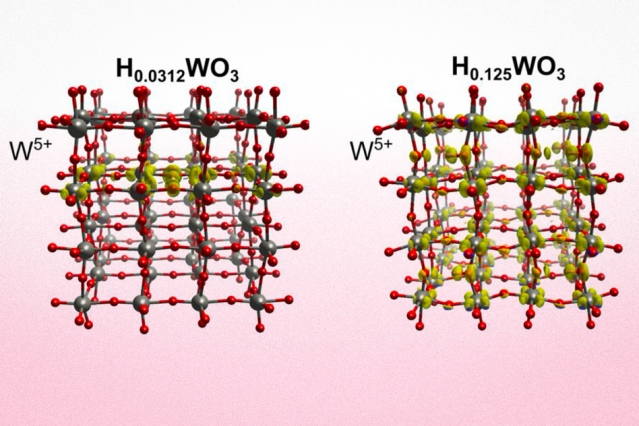
A new system developed at MIT and Brookhaven National Lab could provide a faster, more reliable and much more energy efficient approach to physical neural networks, by using analog ionic-electronic devices to mimic synapses.. Courtesy of the researchers

A June 19, 2020 MIT news release, which originated the news item, provides more insight into this specific piece of research (hint: it’s about energy use and repeatability),

Neural networks attempt to simulate the way learning takes place in the brain, which is based on the gradual strengthening or weakening of the connections between neurons, known as synapses. The core component of this physical neural network is the resistive switch, whose electronic conductance can be controlled electrically. This control, or modulation, emulates the strengthening and weakening of synapses in the brain.

In neural networks using conventional silicon microchip technology, the simulation of these synapses is a very energy-intensive process. To improve efficiency and enable more ambitious neural network goals, researchers in recent years have been exploring a number of physical devices that could more directly mimic the way synapses gradually strengthen and weaken during learning and forgetting.

Most candidate analog resistive devices so far for such simulated synapses have either been very inefficient, in terms of energy use, or performed inconsistently from one device to another or one cycle to the next. The new system, the researchers say, overcomes both of these challenges. “We’re addressing not only the energy challenge, but also the repeatability-related challenge that is pervasive in some of the existing concepts out there,” says Yildiz, who is a professor of nuclear science and engineering and of materials science and engineering.

“I think the bottleneck today for building [neural network] applications is energy efficiency. It just takes too much energy to train these systems, particularly for applications on the edge, like autonomous cars,” says del Alamo, who is the Donner Professor in the Department of Electrical Engineering and Computer Science. Many such demanding applications are simply not feasible with today’s technology, he adds.

The resistive switch in this work is an electrochemical device, which is made of tungsten trioxide (WO3) and works in a way similar to the charging and discharging of batteries. Ions, in this case protons, can migrate into or out of the crystalline lattice of the material,  explains Yildiz, depending on the polarity and strength of an applied voltage. These changes remain in place until altered by a reverse applied voltage — just as the strengthening or weakening of synapses does.

The mechanism is similar to the doping of semiconductors,” says Li, who is also a professor of nuclear science and engineering and of materials science and engineering. In that process, the conductivity of silicon can be changed by many orders of magnitude by introducing foreign ions into the silicon lattice. “Traditionally those ions were implanted at the factory,” he says, but with the new device, the ions are pumped in and out of the lattice in a dynamic, ongoing process. The researchers can control how much of the “dopant” ions go in or out by controlling the voltage, and “we’ve demonstrated a very good repeatability and energy efficiency,” he says.

Yildiz adds that this process is “very similar to how the synapses of the biological brain work. There, we’re not working with protons, but with other ions such as calcium, potassium, magnesium, etc., and by moving those ions you actually change the resistance of the synapses, and that is an element of learning.” The process taking place in the tungsten trioxide in their device is similar to the resistance modulation taking place in biological synapses, she says.

“What we have demonstrated here,” Yildiz says, “even though it’s not an optimized device, gets to the order of energy consumption per unit area per unit change in conductance that’s close to that in the brain.” Trying to accomplish the same task with conventional CMOS type semiconductors would take a million times more energy, she says.

The materials used in the demonstration of the new device were chosen for their compatibility with present semiconductor manufacturing systems, according to Li. But they include a polymer material that limits the device’s tolerance for heat, so the team is still searching for other variations of the device’s proton-conducting membrane and better ways of encapsulating its hydrogen source for long-term operations.

“There’s a lot of fundamental research to be done at the materials level for this device,” Yildiz says. Ongoing research will include “work on how to integrate these devices with existing CMOS transistors” adds del Alamo. “All that takes time,” he says, “and it presents tremendous opportunities for innovation, great opportunities for our students to launch their careers.”

Coincidentally or not a University of Massachusetts at Amherst team announced memristor voltage use comparable to human brain voltage use (see my June 15, 2020 posting), plus, there’s a team at Stanford University touting their low-energy biohybrid synapse in a XXX posting. (June 2020 has been a particularly busy month here for ‘artificial brain’ or ‘memristor’ stories.)

Getting back to this latest MIT research, here’s a link to and a citation for the paper,

Protonic solid-state electrochemical synapse for physical neural networks by Xiahui Yao, Konstantin Klyukin, Wenjie Lu, Murat Onen, Seungchan Ryu, Dongha Kim, Nicolas Emond, Iradwikanari Waluyo, Adrian Hunt, Jesús A. del Alamo, Ju Li & Bilge Yildiz. Nature Communications volume 11, Article number: 3134 (2020) DOI: https://doi.org/10.1038/s41467-020-16866-6 Published: 19 June 2020

This paper is open access.

Innerspace of a nanoparticle

A Jan. 3, 2019 news item on ScienceDaily touts a new means of transporting DNA-coated nanoparticles (DNA is deoxyribonucleic acid),

This holiday season, scientists at the Center for Functional Nanomaterials (CFN) — a U.S. Department of Energy Office of Science User Facility at Brookhaven National Laboratory — have wrapped a box of a different kind. Using a one-step chemical synthesis method, they engineered hollow metallic nanosized boxes with cube-shaped pores at the corners and demonstrated how these “nanowrappers” can be used to carry and release DNA-coated nanoparticles in a controlled way. The research is reported in a paper published on Dec. 12 [2018] in ACS Central Science, a journal of the American Chemical Society (ACS).

A January 3, 2018 Brookhaven National Laboratory (BNL) news release (also on EurekAlert), which originated the news item, explains the work in more detail (Note: Links have been removed),

“Imagine you have a box but you can only use the outside and not the inside,” said co-author Oleg Gang, leader of the CFN Soft and Bio Nanomaterials Group. “This is how we’ve been dealing with nanoparticles. Most nanoparticle assembly or synthesis methods produce solid nanostructures. We need methods to engineer the internal space of these structures.

“Compared to their solid counterparts, hollow nanostructures have different optical and chemical properties that we would like to use for biomedical, sensing, and catalytic applications,” added corresponding author Fang Lu, a scientist in Gang’s group. “In addition, we can introduce surface openings in the hollow structures where materials such as drugs, biological molecules, and even nanoparticles can enter and exit, depending on the surrounding environment.”

Synthetic strategies have been developed to produce hollow nanostructures with surface pores, but typically the size, shape, and location of these pores cannot be well-controlled. The pores are randomly distributed across the surface, resulting in a Swiss-cheese-like structure. A high level of control over surface openings is needed in order to use nanostructures in practical applications–for example, to load and release nanocargo

In this study, the scientists demonstrated a new pathway for chemically sculpturing gold-silver alloy nanowrappers with cube-shaped corner holes from solid nanocube particles. They used a chemical reaction known as nanoscale galvanic replacement. During this reaction, the atoms in a silver nanocube get replaced by gold ions in an aqueous solution at room temperature. The scientists added a molecule (surfactant, or surface-capping agent) to the solution to direct the leaching of silver and the deposition of gold on specific crystalline facets.

“The atoms on the faces of the cube are arranged differently from those in the corners, and thus different atomic planes are exposed, so the galvanic reaction may not proceed the same way in both areas,” explained Lu. “The surfactant we chose binds to the silver surface just enough–not too strongly or weakly–so that gold and silver can interact. Additionally, the absorption of surfactant is relatively weak on the silver cube’s corners, so the reaction is most active here. The silver gets “eaten” away from its edges, resulting in the formation of corner holes, while gold gets deposited on the rest of the surface to create a gold and silver shell.”

To capture the structural and chemical composition changes of the overall structure at the nanoscale in 3-D and at the atomic level in 2-D as the reaction proceeded over three hours, the scientists used electron microscopes at the CFN. The 2-D electron microscope images with energy-dispersive X-ray spectroscopy (EDX) elemental mapping confirmed that the cubes are hollow and composed of a gold-silver alloy. The 3-D images they obtained through electron tomography revealed that these hollow cubes feature large cube-shaped holes at the corners

“In electron tomography, 2-D images collected at different angles are combined to reconstruct an image of an object in 3-D,” said Gang. “The technique is similar to a CT [computerized tomography] scan used to image internal body structures, but it is carried out on a much smaller size scale and uses electrons instead of x-rays.”

The scientists also confirmed the transformation of nanocubes to nanowrappers through spectroscopy experiments capturing optical changes. The spectra showed that the optical absorption of the nanowrappers can be tuned depending on the reaction time. At their final state, the nanowrappers absorb infrared light.

“The absorption spectrum showed a peak at 1250 nanometers, one of the longest wavelengths reported for nanoscale gold or silver,” said Gang. “Typically, gold and silver nanostructures absorb visible light. However, for various applications, we would like those particles to absorb infrared light–for example, in biomedical applications such as phototherapy.”

Using the synthesized nanowrappers, the scientists then demonstrated how spherical gold nanoparticles of an appropriate size that are capped with DNA could be loaded into and released from the corner openings by changing the concentration of salt in the solution. DNA is negatively charged (owing to the oxygen atoms in its phosphate backbone) and changes its configuration in response to increasing or decreasing concentrations of a positively charged ion such as salt. In high salt concentrations, DNA chains contract because their repulsion is reduced by the salt ions. In low salt concentrations, DNA chains stretch because their repulsive forces push them apart.

When the DNA strands contract, the nanoparticles become small enough to fit in the openings and enter the hollow cavity. The nanoparticles can then be locked within the nanowrapper by decreasing the salt concentration. At this lower concentration, the DNA strands stretch, thereby making the nanoparticles too large to go through the pores. The nanoparticles can leave the structure through a reverse process of increasing and decreasing the salt concentration.

“Our electron microscopy and optical spectroscopy studies confirmed that the nanowrappers can be used to load and release nanoscale components,” said Lu. “In principle, they could be used to release optically or chemically active nanoparticles in particular environments, potentially by changing other parameters such as pH or temperature.”

Going forward, the scientists are interested in assembling the nanowrappers into larger-scale architectures, extending their method to other bimetallic systems, and comparing the internal and external catalytic activity of the nanowrappers.

“We did not expect to see such regular, well-defined holes,” said Gang. “Usually, this level of control is quite difficult to achieve for nanoscale objects. Thus, our discovery of this new pathway of nanoscale structure formation is very exciting. The ability to engineer nano-objects with a high level of control is important not only to understanding why certain processes are happening but also to constructing targeted nanostructures for various applications, from nanomedicine and optics to smart materials and catalysis. Our new synthesis method opens up unique opportunities in these areas.”

“This work was made possible by the world-class expertise in nanomaterial synthesis and capabilities that exist at the CFN,” said CFN Director Charles Black. “In particular, the CFN has a leading program in the synthesis of new materials by assembly of nanoscale components, and state-of-the-art electron microscopy and optical spectroscopy capabilities for studying the 3-D structure of these materials and their interaction with light. All of these characterization capabilities are available to the nanoscience research community through the CFN user program. We look forward to seeing the advances in nano-assembly that emerge as scientists across academia, industry, and government make use of the capabilities in their research.”

Here’s a link to and a citation for the paper,

Tailoring Surface Opening of Hollow Nanocubes and Their Application as Nanocargo Carriers by Fang Lu, Huolin Xin, Weiwei Xia, Mingzhao Liu, Yugang Zhang, Weiping Cai, and Oleg Gang. ACS Cent. Sci., 2018, 4 (12), pp 1742–1750 DOI: 10.1021/acscentsci.8b00778 Publication Date (Web): December 12, 2018

Copyright © 2018 American Chemical Society

This paper is open access.

Borophene and next generation electronics?

2D materials as signified by the ‘ene’ suffix are, as far as I can tell, always associated with electronics—initially. Borophene is not an exception.

This borophene news was announced in a December 3, 2018 news item on ScienceDaily,

Borophene — two-dimensional (2-D) atom-thin-sheets of boron, a chemical element traditionally found in fiberglass insulation — is anything but boring. Though boron is a nonmetallic semiconductor in its bulk (3-D) form, it becomes a metallic conductor in 2-D. Borophene is extremely flexible, strong, and lightweight — even more so than its carbon-based analogue, graphene. [Providing a little competition to the Europeans who are seriously pursuing nanotechnology-enabled electronics and other applications with graphene?] These unique electronic and mechanical properties make borophene a promising material platform for next-generation electronic devices such as wearables, biomolecule sensors, light detectors, and quantum computers.

Now, physicists from the U.S. Department of Energy’s (DOE) Brookhaven National Laboratory and Yale University have synthesized borophene on copper substrates with large-area (ranging in size from 10 to 100 micrometers) single-crystal domains (for reference, a strand of human hair is about 100 micrometers wide). Previously, only nanometer-size single-crystal flakes of borophene had been produced. The advance, reported on Dec. 3 [2018] in Nature Nanotechnology, represents an important step in making practical borophene-based devices possible.

A December 3, 2018 Brookhaven National Laboratory (BNL) news release (also on EurekAlert), which originated the news item, provides more detail about 2D materials and the specifics of this borophene research,

For electronic applications, high-quality single crystals–periodic arrangements of atoms that continue throughout the entire crystal lattice without boundaries or defects–must be distributed over large areas of the surface material (substrate) on which they are grown. For example, today’s microchips use single crystals of silicon and other semiconductors. Device fabrication also requires an understanding of how different substrates and growth conditions impact a material’s crystal structure, which determines its properties.

“We increased the size of the single-crystal domains by a factor of a million,” said co-author and project lead Ivan Bozovic, senior scientist and Molecular Beam Epitaxy Group Leader in Brookhaven Lab’s Condensed Matter Physics and Materials Science (CMPMS) Department and adjunct professor of applied physics at Yale University. “Large domains are required to fabricate next-generation electronic devices with high electron mobility. Electrons that can easily and quickly move through a crystal structure are key to improving device performance.”

A new 2-D material

Since the 2004 discovery of graphene–a single sheet of carbon atoms, which can be peeled from graphite, the core component of pencils, with Scotch tape–scientists have been on the hunt for other 2-D materials with remarkable properties. The chemical bonds between carbon atoms that impart graphene with its strength make manipulating its structure difficult.

Theorists predicted that boron (next to carbon on the Periodic Table, with one less electron) deposited on an appropriately chosen substrate could form a 2-D material similar to graphene. But this prediction was not experimentally confirmed until three years ago, when scientists synthesized borophene for the very first time. They deposited boron onto silver substrates under ultrahigh-vacuum conditions through molecular beam epitaxy (MBE), a precisely controlled atomic layer-by-layer crystal growth technique. Soon thereafter, another group of scientists grew borophene on silver, but they proposed an entirely different crystal structure.

“Borophene is structurally similar to graphene, with a hexagonal network made of boron (instead of carbon) atoms on each of the six vertices defining the hexagon,” said Bozovic. “However, borophene is different in that it periodically has an extra boron atom in the center of the hexagon. The crystal structure tends to be theoretically stable when about four out of every five center positions are occupied and one is vacant.”

According to theory, while the number of vacancies is fixed, their arrangement is not. As long as the vacancies are distributed in a way that maintains the most stable (lowest energy) structure, they can be rearranged. Because of this flexibility, borophene can have multiple configurations.

A small step toward device fabrication

In this study, the scientists first investigated the real-time growth of borophene on silver surfaces at various temperatures. They grew the samples at Yale in an ultra-high vacuum low-energy electron microscope (LEEM) equipped with an MBE system. During and after the growth process, they bombarded the sample with a beam of electrons at low energy and analyzed the low-energy electron diffraction (LEED) patterns produced as electrons were reflected from the crystal surface and projected onto a detector. Because the electrons have low energy, they can only reach the first few atomic layers of the material. The distance between the reflected electrons (“spots” in the diffraction patterns) is related to the distance between atoms on the surface, and from this information, scientists can reconstruct the crystal structure.

In this case, the patterns revealed that the single-crystal borophene domains were only tens of nanometers in size–too small for fabricating devices and studying fundamental physical properties–for all growth conditions. They also resolved the controversy about borophene’s structure: both structures exist, but they form at different temperatures. The scientists confirmed their LEEM and LEED results through atomic force microscopy (AFM). In AFM, a sharp tip is scanned over a surface, and the measured force between the tip and atoms on the surface is used to map the atomic arrangement.

To promote the formation of larger crystals, the scientists then switched the substrate from silver to copper, applying the same LEEM, LEED, and AFM techniques. Brookhaven scientists Percy Zahl and Ilya Drozdov also imaged the surface structure at high resolution using a custom-built scanning tunneling microscope (STM) with a carbon monoxide probe tip at Brookhaven’s Center for Functional Nanomaterials (CFN)–a U.S. Department of Energy (DOE) Office of Science User Facility. Yale theorists Stephen Eltinge and Sohrab Ismail-Beigi performed calculations to determine the stability of the experimentally obtained structures. After identifying which structures were most stable, they simulated the electron diffraction spectra and STM images and compared them to the experimental data. This iterative process continued until theory and experiment were in agreement.

“From theoretical insights, we expected copper to produce larger single crystals because it interacts more strongly with borophene than silver,” said Bozovic. “Copper donates some electrons to stabilize borophene, but the materials do not interact too much as to form a compound. Not only are the single crystals larger, but the structures of borophene on copper are different from any of those grown on silver.”

Because there are several possible distributions of vacancies on the surface, various crystal structures of borophene can emerge. This study also showed how the structure of borophene can be modified by changing the substrate and, in some cases, the temperature or deposition rate.

The next step is to transfer the borophene sheets from the metallic copper surfaces to insulating device-compatible substrates. Then, scientists will be able to accurately measure resistivity and other electrical properties important to device functionality. Bozovic is particularly excited to test whether borophene can be made superconducting. Some theorists have speculated that its unusual electronic structure may even open a path to lossless transmission of electricity at room temperature, as opposed to the ultracold temperatures usually required for superconductivity. Ultimately, the goal in 2-D materials research is to be able to fine-tune the properties of these materials to suit particular applications.

Here’s a link to and a citation for the paper,

Large-area single-crystal sheets of borophene on Cu(111) surfaces by Rongting Wu, Ilya K. Drozdov, Stephen Eltinge, Percy Zahl, Sohrab Ismail-Beigi, Ivan Božović & Adrian Gozar. Nature Nanotechnology (2018) DOI: https://doi.org/10.1038/s41565-018-0317-6Published 03 December 2018

This paper is behind a paywall.

Cleaning up nuclear waste gases with nanotechnology-enabled materials

Swiss and US scientists have developed a nanoporous crystal that could be used to clean up nuclear waste gases according to a June 13, 2016 news item on Nanowerk (Note: A link has been removed),

An international team of scientists at EPFL [École polytechnique fédérale de Lausanne in Switzerland] and the US have discovered a material that can clear out radioactive waste from nuclear plants more efficiently, cheaply, and safely than current methods.

Nuclear energy is one of the cheapest alternatives to carbon-based fossil fuels. But nuclear-fuel reprocessing plants generate waste gas that is currently too expensive and dangerous to deal with. Scanning hundreds of thousands of materials, scientists led by EPFL and their US colleagues have now discovered a material that can absorb nuclear waste gases much more efficiently, cheaply and safely. The work is published in Nature Communications (“Metal–organic framework with optimally selective xenon adsorption and separation”).

A June 14, 2016 EPFL press release (also on EurekAlert), which originated the news item, explains further,

Nuclear-fuel reprocessing plants generate volatile radionuclides such as xenon and krypton, which escape in the so-called “off-gas” of these facilities – the gases emitted as byproducts of the chemical process. Current ways of capturing and clearing out these gases involve distillation at very low temperatures, which is expensive in both terms of energy and capital costs, and poses a risk of explosion.

Scientists led by Berend Smit’s lab at EPFL (Sion) and colleagues in the US, have now identified a material that can be used as an efficient, cheaper, and safer alternative to separate xenon and krypton – and at room temperature. The material, abbreviated as SBMOF-1, is a nanoporous crystal and belongs a class of materials that are currently used to clear out CO2 emissions and other dangerous pollutants. These materials are also very versatile, and scientists can tweak them to self-assemble into ordered, pre-determined crystal structures. In this way, they can synthesize millions of tailor-made materials that can be optimized for gas storage separation, catalysis, chemical sensing and optics.

The scientists carried out high-throughput screening of large material databases of over 125,000 candidates. To do this, they used molecular simulations to find structures that can separate xenon and krypton, and under conditions that match those involved in reprocessing nuclear waste.

Because xenon has a much shorter half-life than krypton – a month versus a decade – the scientists had to find a material that would be selective for both but would capture them separately. As xenon is used in commercial lighting, propulsion, imaging, anesthesia and insulation, it can also be sold back into the chemical market to offset costs.

The scientists identified and confirmed that SBMOF-1 shows remarkable xenon capturing capacity and xenon/krypton selectivity under nuclear-plant conditions and at room temperature.

The US partners have also made an announcement with this June 13, 2016 Pacific Northwest National Laboratory (PNNL) news release (also on EurekAlert), Note: It is a little repetitive but there’s good additional information,

Researchers are investigating a new material that might help in nuclear fuel recycling and waste reduction by capturing certain gases released during reprocessing. Conventional technologies to remove these radioactive gases operate at extremely low, energy-intensive temperatures. By working at ambient temperature, the new material has the potential to save energy, make reprocessing cleaner and less expensive. The reclaimed materials can also be reused commercially.

Appearing in Nature Communications, the work is a collaboration between experimentalists and computer modelers exploring the characteristics of materials known as metal-organic frameworks.

“This is a great example of computer-inspired material discovery,” said materials scientist Praveen Thallapally of the Department of Energy’s Pacific Northwest National Laboratory. “Usually the experimental results are more realistic than computational ones. This time, the computer modeling showed us something the experiments weren’t telling us.”

Waste avoidance

Recycling nuclear fuel can reuse uranium and plutonium — the majority of the used fuel — that would otherwise be destined for waste. Researchers are exploring technologies that enable safe, efficient, and reliable recycling of nuclear fuel for use in the future.

A multi-institutional, international collaboration is studying materials to replace costly, inefficient recycling steps. One important step is collecting radioactive gases xenon and krypton, which arise during reprocessing. To capture xenon and krypton, conventional technologies use cryogenic methods in which entire gas streams are brought to a temperature far below where water freezes — such methods are energy intensive and expensive.

Thallapally, working with Maciej Haranczyk and Berend Smit of Lawrence Berkeley National Laboratory [LBNL] and others, has been studying materials called metal-organic frameworks, also known as MOFs, that could potentially trap xenon and krypton without having to use cryogenics.

These materials have tiny pores inside, so small that often only a single molecule can fit inside each pore. When one gas species has a higher affinity for the pore walls than other gas species, metal-organic frameworks can be used to separate gaseous mixtures by selectively adsorbing.

To find the best MOF for xenon and krypton separation, computational chemists led by Haranczyk and Smit screened 125,000 possible MOFs for their ability to trap the gases. Although these gases can come in radioactive varieties, they are part of a group of chemically inert elements called “noble gases.” The team used computing resources at NERSC, the National Energy Research Scientific Computing Center, a DOE Office of Science User Facility at LBNL.

“Identifying the optimal material for a given process, out of thousands of possible structures, is a challenge due to the sheer number of materials. Given that the characterization of each material can take up to a few hours of simulations, the entire screening process may fill a supercomputer for weeks,” said Haranczyk. “Instead, we developed an approach to assess the performance of materials based on their easily computable characteristics. In this case, seven different characteristics were necessary for predicting how the materials behaved, and our team’s grad student Cory Simon’s application of machine learning techniques greatly sped up the material discovery process by eliminating those that didn’t meet the criteria.”

The team’s models identified the MOF that trapped xenon most selectively and had a pore size close to the size of a xenon atom — SBMOF-1, which they then tested in the lab at PNNL.

After optimizing the preparation of SBMOF-1, Thallapally and his team at PNNL tested the material by running a mixture of gases through it — including a non-radioactive form of xenon and krypton — and measuring what came out the other end. Oxygen, helium, nitrogen, krypton, and carbon dioxide all beat xenon out. This indicated that xenon becomes trapped within SBMOF-1’s pores until the gas saturates the material.

Other tests also showed that in the absence of xenon, SBMOF-1 captures krypton. During actual separations, then, operators would pass the gas streams through SBMOF-1 twice to capture both gases.

The team also tested SBMOF-1’s ability to hang onto xenon in conditions of high humidity. Humidity interferes with cryogenics, and gases must be dehydrated before putting them through the ultra-cold method, another time-consuming expense. SBMOF-1, however, performed quite admirably, retaining more than 85 percent of the amount of xenon in high humidity as it did in dry conditions.

The final step in collecting xenon or krypton gas would be to put the MOF material under a vacuum, which sucks the gas out of the molecular cages for safe storage. A last laboratory test examined how stable the material was by repeatedly filling it up with xenon gas and then vacuuming out the xenon. After 10 cycles of this, SBMOF-1 collected just as much xenon as the first cycle, indicating a high degree of stability for long-term use.

Thallapally attributes this stability to the manner in which SBMOF-1 interacts with xenon. Rather than chemical reactions between the molecular cages and the gases, the relationship is purely physical. The material can last a lot longer without constantly going through chemical reactions, he said.

A model finding

Although the researchers showed that SBMOF-1 is a good candidate for nuclear fuel reprocessing, getting these results wasn’t smooth sailing. In the lab, the researchers had followed a previously worked out protocol from Stony Brook University to prepare SBMOF-1. Part of that protocol requires them to “activate” SBMOF-1 by heating it up to 300 degrees Celsius, three times the temperature of boiling water.

Activation cleans out material left in the pores from MOF synthesis. Laboratory tests of the activated SBMOF-1, however, showed the material didn’t behave as well as it should, based on the computer modeling results.

The researchers at PNNL repeated the lab experiments. This time, however, they activated SBMOF-1 at a lower temperature, 100 degrees Celsius, or the actual temperature of boiling water. Subjecting the material to the same lab tests, the researchers found SBMOF-1 behaving as expected, and better than at the higher activation temperature.

But why? To figure out where the discrepancy came from, the researchers modeled what happened to SBMOF-1 at 300 degrees Celsius. Unexpectedly, the pores squeezed in on themselves.

“When we heated the crystal that high, atoms within the pore tilted and partially blocked the pores,” said Thallapally. “The xenon doesn’t fit.”

Armed with these new computational and experimental insights, the researchers can explore SBMOF-1 and other MOFs further for nuclear fuel recycling. These MOFs might also be able to capture other noble gases such as radon, a gas known to pool in some basements.

Researchers hailed from several other institutions as well as those listed earlier, including University of California, Berkeley, Ecole Polytechnique Fédérale de Lausanne (EPFL) in Switzerland, Brookhaven National Laboratory, and IMDEA Materials Institute in Spain. This work was supported by the [US] Department of Energy Offices of Nuclear Energy and Science.

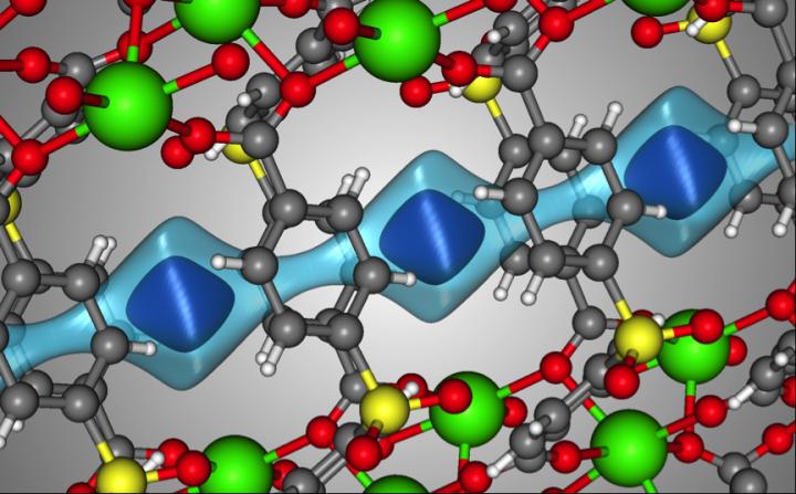
Here’s an image the researchers have provided to illustrate their work,

Caption: The crystal structure of SBMOF-1 (green = Ca, yellow = S, red = O, gray = C, white = H). The light blue surface is a visualization of the one-dimensional channel that SBMOF-1 creates for the gas molecules to move through. The darker blue surface illustrates where a Xe atom sits in the pores of SBMOF-1 when it adsorbs. Credit: Berend Smit/EPFL/University of California Berkley

Caption: The crystal structure of SBMOF-1 (green = Ca, yellow = S, red = O, gray = C, white = H). The light blue surface is a visualization of the one-dimensional channel that SBMOF-1 creates for the gas molecules to move through. The darker blue surface illustrates where a Xe atom sits in the pores of SBMOF-1 when it adsorbs. Credit: Berend Smit/EPFL/University of California Berkley

Here’s a link to and a citation for the paper,

Metal–organic framework with optimally selective xenon adsorption and separation by Debasis Banerjee, Cory M. Simon, Anna M. Plonka, Radha K. Motkuri, Jian Liu, Xianyin Chen, Berend Smit, John B. Parise, Maciej Haranczyk, & Praveen K. Thallapally. Nature Communications 7, Article number: ncomms11831  doi:10.1038/ncomms11831 Published 13 June 2016

This paper is open access.

Final comment, this is the second time in the last month I’ve stumbled across more positive approaches to nuclear energy. The first time was a talk (Why Nuclear Power is Necessary) held in Vancouver, Canada in May 2016 (details here). I’m not trying to suggest anything unduly sinister but it is interesting since most of my adult life nuclear power has been viewed with fear and suspicion.