Tag Archives: carbon atoms

Cannibalisitic nanostructures

I think this form of ‘cannibalism’ could also be described as a form of ‘self-assembly’. That said, here is an August 31, 2018 news item on ScienceDaily announcing ‘cannibalistic’ materials,

Scientists at the [US] Department of Energy’s [DOE] Oak Ridge National Laboratory [ORNL] induced a two-dimensional material to cannibalize itself for atomic “building blocks” from which stable structures formed.

The findings, reported in Nature Communications, provide insights that may improve design of 2D materials for fast-charging energy-storage and electronic devices.

An August 31, 2018 DOE/Oak Ridge National Laboratory news release (also on EurekAlert), which originated the news item, provides more detail (Note: Links have been removed),

“Under our experimental conditions, titanium and carbon atoms can spontaneously form an atomically thin layer of 2D transition-metal carbide, which was never observed before,” said Xiahan Sang of ORNL.

He and ORNL’s Raymond Unocic led a team that performed in situ experiments using state-of-the-art scanning transmission electron microscopy (STEM), combined with theory-based simulations, to reveal the mechanism’s atomistic details.

“This study is about determining the atomic-level mechanisms and kinetics that are responsible for forming new structures of a 2D transition-metal carbide such that new synthesis methods can be realized for this class of materials,” Unocic added.

The starting material was a 2D ceramic called a MXene (pronounced “max een”). Unlike most ceramics, MXenes are good electrical conductors because they are made from alternating atomic layers of carbon or nitrogen sandwiched within transition metals like titanium.

The research was a project of the Fluid Interface Reactions, Structures and Transport (FIRST) Center, a DOE Energy Frontier Research Center that explores fluid–solid interface reactions that have consequences for energy transport in everyday applications. Scientists conducted experiments to synthesize and characterize advanced materials and performed theory and simulation work to explain observed structural and functional properties of the materials. New knowledge from FIRST projects provides guideposts for future studies.

The high-quality material used in these experiments was synthesized by Drexel University scientists, in the form of five-ply single-crystal monolayer flakes of MXene. The flakes were taken from a parent crystal called “MAX,” which contains a transition metal denoted by “M”; an element such as aluminum or silicon, denoted by “A”; and either a carbon or nitrogen atom, denoted by “X.” The researchers used an acidic solution to etch out the monoatomic aluminum layers, exfoliate the material and delaminate it into individual monolayers of a titanium carbide MXene (Ti3C2).

The ORNL scientists suspended a large MXene flake on a heating chip with holes drilled in it so no support material, or substrate, interfered with the flake. Under vacuum, the suspended flake was exposed to heat and irradiated with an electron beam to clean the MXene surface and fully expose the layer of titanium atoms.

MXenes are typically inert because their surfaces are covered with protective functional groups—oxygen, hydrogen and fluorine atoms that remain after acid exfoliation. After protective groups are removed, the remaining material activates. Atomic-scale defects—“vacancies” created when titanium atoms are removed during etching—are exposed on the outer ply of the monolayer. “These atomic vacancies are good initiation sites,” Sang said. “It’s favorable for titanium and carbon atoms to move from defective sites to the surface.” In an area with a defect, a pore may form when atoms migrate.

“Once those functional groups are gone, now you’re left with a bare titanium layer (and underneath, alternating carbon, titanium, carbon, titanium) that’s free to reconstruct and form new structures on top of existing structures,” Sang said.

High-resolution STEM imaging proved that atoms moved from one part of the material to another to build structures. Because the material feeds on itself, the growth mechanism is cannibalistic.

“The growth mechanism is completely supported by density functional theory and reactive molecular dynamics simulations, thus opening up future possibilities to use these theory tools to determine the experimental parameters required for synthesizing specific defect structures,” said Adri van Duin of Penn State [Pennsylvania State University].

Most of the time, only one additional layer [of carbon and titanium] grew on a surface. The material changed as atoms built new layers. Ti3C2 turned into Ti4C3, for example.

“These materials are efficient at ionic transport, which lends itself well to battery and supercapacitor applications,” Unocic said. “How does ionic transport change when we add more layers to nanometer-thin MXene sheets?” This question may spur future studies.

“Because MXenes containing molybdenum, niobium, vanadium, tantalum, hafnium, chromium and other metals are available, there are opportunities to make a variety of new structures containing more than three or four metal atoms in cross-section (the current limit for MXenes produced from MAX phases),” Yury Gogotsi of Drexel University added. “Those materials may show different useful properties and create an array of 2D building blocks for advancing technology.”

At ORNL’s Center for Nanophase Materials Sciences (CNMS), Yu Xie, Weiwei Sun and Paul Kent performed first-principles theory calculations to explain why these materials grew layer by layer instead of forming alternate structures, such as squares. Xufan Li and Kai Xiao helped understand the growth mechanism, which minimizes surface energy to stabilize atomic configurations. Penn State scientists conducted large-scale dynamical reactive force field simulations showing how atoms rearranged on surfaces, confirming defect structures and their evolution as observed in experiments.

The researchers hope the new knowledge will help others grow advanced materials and generate useful nanoscale structures.

Here’s a link to and a citation for the paper,

In situ atomistic insight into the growth mechanisms of single layer 2D transition metal carbides by Xiahan Sang, Yu Xie, Dundar E. Yilmaz, Roghayyeh Lotfi, Mohamed Alhabeb, Alireza Ostadhossein, Babak Anasori, Weiwei Sun, Xufan Li, Kai Xiao, Paul R. C. Kent, Adri C. T. van Duin, Yury Gogotsi, & Raymond R. Unocic. Nature Communicationsvolume 9, Article number: 2266 (2018) DOI: https://doi.org/10.1038/s41467-018-04610-0 Published 11 June 2018

This paper is open access.
If only AI had a brain (a Wizard of Oz reference?)

The title, which I’ve borrowed from the news release, is the only Wizard of Oz reference that I can find but it works so well, you don’t really need anything more.

Moving onto the news, a July 23, 2018 news item on phys.org announces new work on developing an artificial synapse (Note: A link has been removed),

Digital computation has rendered nearly all forms of analog computation obsolete since as far back as the 1950s. However, there is one major exception that rivals the computational power of the most advanced digital devices: the human brain.

The human brain is a dense network of neurons. Each neuron is connected to tens of thousands of others, and they use synapses to fire information back and forth constantly. With each exchange, the brain modulates these connections to create efficient pathways in direct response to the surrounding environment. Digital computers live in a world of ones and zeros. They perform tasks sequentially, following each step of their algorithms in a fixed order.

A team of researchers from Pitt’s [University of Pittsburgh] Swanson School of Engineering have developed an “artificial synapse” that does not process information like a digital computer but rather mimics the analog way the human brain completes tasks. Led by Feng Xiong, assistant professor of electrical and computer engineering, the researchers published their results in the recent issue of the journal Advanced Materials (DOI: 10.1002/adma.201802353). His Pitt co-authors include Mohammad Sharbati (first author), Yanhao Du, Jorge Torres, Nolan Ardolino, and Minhee Yun.

A July 23, 2018 University of Pittsburgh Swanson School of Engineering news release (also on EurekAlert), which originated the news item, provides further information,

“The analog nature and massive parallelism of the brain are partly why humans can outperform even the most powerful computers when it comes to higher order cognitive functions such as voice recognition or pattern recognition in complex and varied data sets,” explains Dr. Xiong.

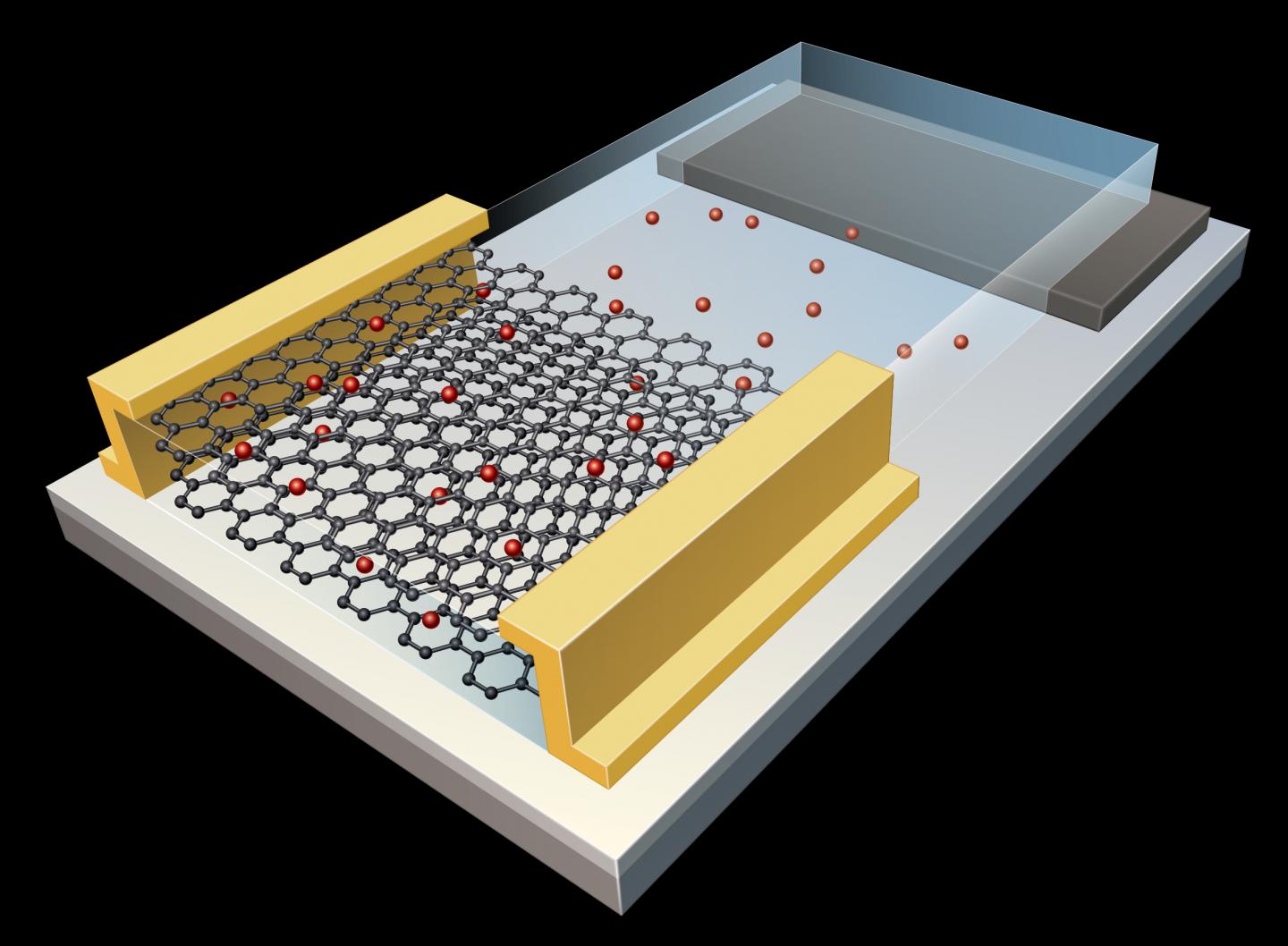
An emerging field called “neuromorphic computing” focuses on the design of computational hardware inspired by the human brain. Dr. Xiong and his team built graphene-based artificial synapses in a two-dimensional honeycomb configuration of carbon atoms. Graphene’s conductive properties allowed the researchers to finely tune its electrical conductance, which is the strength of the synaptic connection or the synaptic weight. The graphene synapse demonstrated excellent energy efficiency, just like biological synapses.

In the recent resurgence of artificial intelligence, computers can already replicate the brain in certain ways, but it takes about a dozen digital devices to mimic one analog synapse. The human brain has hundreds of trillions of synapses for transmitting information, so building a brain with digital devices is seemingly impossible, or at the very least, not scalable. Xiong Lab’s approach provides a possible route for the hardware implementation of large-scale artificial neural networks.

According to Dr. Xiong, artificial neural networks based on the current CMOS (complementary metal-oxide semiconductor) technology will always have limited functionality in terms of energy efficiency, scalability, and packing density. “It is really important we develop new device concepts for synaptic electronics that are analog in nature, energy-efficient, scalable, and suitable for large-scale integrations,” he says. “Our graphene synapse seems to check all the boxes on these requirements so far.”

With graphene’s inherent flexibility and excellent mechanical properties, these graphene-based neural networks can be employed in flexible and wearable electronics to enable computation at the “edge of the internet”–places where computing devices such as sensors make contact with the physical world.

“By empowering even a rudimentary level of intelligence in wearable electronics and sensors, we can track our health with smart sensors, provide preventive care and timely diagnostics, monitor plants growth and identify possible pest issues, and regulate and optimize the manufacturing process–significantly improving the overall productivity and quality of life in our society,” Dr. Xiong says.

The development of an artificial brain that functions like the analog human brain still requires a number of breakthroughs. Researchers need to find the right configurations to optimize these new artificial synapses. They will need to make them compatible with an array of other devices to form neural networks, and they will need to ensure that all of the artificial synapses in a large-scale neural network behave in the same exact manner. Despite the challenges, Dr. Xiong says he’s optimistic about the direction they’re headed.

“We are pretty excited about this progress since it can potentially lead to the energy-efficient, hardware implementation of neuromorphic computing, which is currently carried out in power-intensive GPU clusters. The low-power trait of our artificial synapse and its flexible nature make it a suitable candidate for any kind of A.I. device, which would revolutionize our lives, perhaps even more than the digital revolution we’ve seen over the past few decades,” Dr. Xiong says.

There is a visual representation of this artificial synapse,

Caption: Pitt engineers built a graphene-based artificial synapse in a two-dimensional, honeycomb configuration of carbon atoms that demonstrated excellent energy efficiency comparable to biological synapses Credit: Swanson School of Engineering

Here’s a link to and a citation for the paper,

Low‐Power, Electrochemically Tunable Graphene Synapses for Neuromorphic Computing by Mohammad Taghi Sharbati, Yanhao Du, Jorge Torres, Nolan D. Ardolino, Minhee Yun, Feng Xiong. Advanced Materials DOP: https://doi.org/10.1002/adma.201802353 First published [online]: 23 July 2018

This paper is behind a paywall.

I did look at the paper and if I understand it rightly, this approach is different from the memristor-based approaches that I have so often featured here. More than that I cannot say.

Finally, the Wizard of Oz song ‘If I Only Had a Brain’,

Creating cheap, small carbon nanotubes

The excitement fairly crackles off the video,

A May 24, 2018 news item on Nanowerk announces the research,

Imagine a box you plug into the wall that cleans your toxic air and pays you cash.

That’s essentially what Vanderbilt University researchers produced after discovering the blueprint for turning the carbon dioxide into carbon nanotubes with small diameters.

Carbon nanotubes are supermaterials that can be stronger than steel and more conductive than copper. The reason they’re not in every application from batteries to tires is that these amazing properties only show up in the tiniest nanotubes, which are extremely expensive. Not only did the Vanderbilt team show they can make these materials from carbon dioxide sucked from the air, but how to do this in a way that is much cheaper than any other method out there.

I’m not sure what ‘small’ means in this context. I’ve heard of long and short carbon nanotubes (CNTs) and also of single-walled, multi-walled, and double-walled CNTs. I wish there’d been an an explanation and measurements for ‘small diameter CNTs’. That nitpick aside, a May 23, 2018 Vanderbilt University news release by Heidi Hall adds a few more technical details,

These materials, which Assistant Professor of Mechanical Engineering Cary Pint calls “black gold,” could steer the conversation from the negative impact of emissions to how we can use them in future technology.

“One of the most exciting things about what we’ve done is use electrochemistry to pull apart carbon dioxide into elemental constituents of carbon and oxygen and stitch together, with nanometer precision, those carbon atoms into new forms of matter,” Pint said. “That opens the door to being able to generate really valuable products with carbon nanotubes.

“These could revolutionize the world.”

In a report published today in ACS [American Chemical Society] Applied Materials and Interfaces, Pint, interdisciplinary material science Ph.D. student Anna Douglas and their team describe how tiny nanoparticles 10,000 times smaller than a human hair can be produced from coatings on stainless steel surfaces. The key was making them small enough to be valuable.

“The cheapest carbon nanotubes on the market cost around $100-200 per kilogram,” Douglas said. “Our research advance demonstrates a pathway to synthesize carbon nanotubes better in quality than these materials with lower cost and using carbon dioxide captured from the air.”

But making small nanotubes is no small task. The research team showed that a process called Ostwald ripening — where the nanoparticles that grow the carbon nanotubes change in size to larger diameters — is a key contender against producing the infinitely more useful size. The team showed they could partially overcome this by tuning electrochemical parameters to minimize these pesky large nanoparticles.

side-by-side photos showing stainless steel plate becoming covered in carbon nanotubes (which look like lumps of ash or mud)
Small diameter carbon nanotubes grown on a stainless steel surface. (Pint Lab/Vanderbilt University)

This core technology led Pint and Douglas to co-found SkyNano LLC, a company focused on building upon the science of this process to scale up and commercialize products from these materials.

“What we’ve learned is the science that opens the door to now build some of the most valuable materials in our world, such as diamonds and single-walled carbon nanotubes, from carbon dioxide that we capture from air through our process,” Pint said.

Here’s a link to and a citation for the paper,

Toward Small-Diameter Carbon Nanotubes Synthesized from Captured Carbon Dioxide: Critical Role of Catalyst Coarsening by Anna Douglas, Rachel Carter, Mengya Li, and Cary L. Pint. ACS Appl. Mater. Interfaces, Article ASAP DOI: 10.1021/acsami.8b02834 Publication Date (Web): May 1, 2018

Copyright © 2018 American Chemical Society

This paper is behind a paywall.

Regarding the start-up, SkyNano, which Douglas and Pint have co-founded, it looks to be at a  very early stage.

Spooling strips of graphene

An April 18, 2018 news item on phys.org highlights an exciting graphene development at the Massachusetts Institute of Technology (MIT),

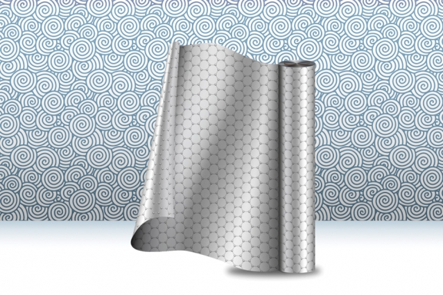
MIT engineers have developed a continuous manufacturing process that produces long strips of high-quality graphene.

The team’s results are the first demonstration of an industrial, scalable method for manufacturing high-quality graphene that is tailored for use in membranes that filter a variety of molecules, including salts, larger ions, proteins, or nanoparticles. Such membranes should be useful for desalination, biological separation, and other applications.

A new manufacturing process produces strips of graphene, at large scale, for use in membrane technologies and other applications. Image: Christine Daniloff, MIT

An April 17, 2018 MIT news release (also on EurekAlert) by Jennifer Chu, which originated the news item,. provides more detail,

“For several years, researchers have thought of graphene as a potential route to ultrathin membranes,” says John Hart, associate professor of mechanical engineering and director of the Laboratory for Manufacturing and Productivity at MIT. “We believe this is the first study that has tailored the manufacturing of graphene toward membrane applications, which require the graphene to be seamless, cover the substrate fully, and be of high quality.”

Hart is the senior author on the paper, which appears online in the journal Applied Materials and Interfaces. The study includes first author Piran Kidambi, a former MIT postdoc who is now an assistant professor at Vanderbilt University; MIT graduate students Dhanushkodi Mariappan and Nicholas Dee; Sui Zhang of the National University of Singapore; Andrey Vyatskikh, a former student at the Skolkovo Institute of Science and Technology who is now at Caltech; and Rohit Karnik, an associate professor of mechanical engineering at MIT.

Growing graphene

For many researchers, graphene is ideal for use in filtration membranes. A single sheet of graphene resembles atomically thin chicken wire and is composed of carbon atoms joined in a pattern that makes the material extremely tough and impervious to even the smallest atom, helium.

Researchers, including Karnik’s group, have developed techniques to fabricate graphene membranes and precisely riddle them with tiny holes, or nanopores, the size of which can be tailored to filter out specific molecules. For the most part, scientists synthesize graphene through a process called chemical vapor deposition, in which they first heat a sample of copper foil and then deposit onto it a combination of carbon and other gases.

Graphene-based membranes have mostly been made in small batches in the laboratory, where researchers can carefully control the material’s growth conditions. However, Hart and his colleagues believe that if graphene membranes are ever to be used commercially they will have to be produced in large quantities, at high rates, and with reliable performance.

“We know that for industrialization, it would need to be a continuous process,” Hart says. “You would never be able to make enough by making just pieces. And membranes that are used commercially need to be fairly big – some so big that you would have to send a poster-wide sheet of foil into a furnace to make a membrane.”

A factory roll-out

The researchers set out to build an end-to-end, start-to-finish manufacturing process to make membrane-quality graphene.

The team’s setup combines a roll-to-roll approach – a common industrial approach for continuous processing of thin foils – with the common graphene-fabrication technique of chemical vapor deposition, to manufacture high-quality graphene in large quantities and at a high rate. The system consists of two spools, connected by a conveyor belt that runs through a small furnace. The first spool unfurls a long strip of copper foil, less than 1 centimeter wide. When it enters the furnace, the foil is fed through first one tube and then another, in a “split-zone” design.

While the foil rolls through the first tube, it heats up to a certain ideal temperature, at which point it is ready to roll through the second tube, where the scientists pump in a specified ratio of methane and hydrogen gas, which are deposited onto the heated foil to produce graphene.

“Graphene starts forming in little islands, and then those islands grow together to form a continuous sheet,” Hart says. “By the time it’s out of the oven, the graphene should be fully covering the foil in one layer, kind of like a continuous bed of pizza.”

As the graphene exits the furnace, it’s rolled onto the second spool. The researchers found that they were able to feed the foil continuously through the system, producing high-quality graphene at a rate of 5 centimers per minute. Their longest run lasted almost four hours, during which they produced about 10 meters of continuous graphene.

“If this were in a factory, it would be running 24-7,” Hart says. “You would have big spools of foil feeding through, like a printing press.”

Flexible design

Once the researchers produced graphene using their roll-to-roll method, they unwound the foil from the second spool and cut small samples out. They cast the samples with a polymer mesh, or support, using a method developed by scientists at Harvard University, and subsequently etched away the underlying copper.

“If you don’t support graphene adequately, it will just curl up on itself,” Kidambi says. “So you etch copper out from underneath and have graphene directly supported by a porous polymer – which is basically a membrane.”

The polymer covering contains holes that are larger than graphene’s pores, which Hart says act as microscopic “drumheads,” keeping the graphene sturdy and its tiny pores open.

The researchers performed diffusion tests with the graphene membranes, flowing a solution of water, salts, and other molecules across each membrane. They found that overall, the membranes were able to withstand the flow while filtering out molecules. Their performance was comparable to graphene membranes made using conventional, small-batch approaches.

The team also ran the process at different speeds, with different ratios of methane and hydrogen gas, and characterized the quality of the resulting graphene after each run. They drew up plots to show the relationship between graphene’s quality and the speed and gas ratios of the manufacturing process. Kidambi says that if other designers can build similar setups, they can use the team’s plots to identify the settings they would need to produce a certain quality of graphene.

“The system gives you a great degree of flexibility in terms of what you’d like to tune graphene for, all the way from electronic to membrane applications,” Kidambi says.

Looking forward, Hart says he would like to find ways to include polymer casting and other steps that currently are performed by hand, in the roll-to-roll system.

“In the end-to-end process, we would need to integrate more operations into the manufacturing line,” Hart says. “For now, we’ve demonstrated that this process can be scaled up, and we hope this increases confidence and interest in graphene-based membrane technologies, and provides a pathway to commercialization.”

Here’s a link to and a citation for the paper,

A Scalable Route to Nanoporous Large-Area Atomically Thin Graphene Membranes by Roll-to-Roll Chemical Vapor Deposition and Polymer Support Casting by Piran R. Kidambi, Dhanushkodi D. Mariappan, Nicholas T. Dee, Andrey Vyatskikh, Sui Zhang, Rohit Karnik, and A. John Hart. ACS Appl. Mater. Interfaces, 2018, 10 (12), pp 10369–10378 DOI: 10.1021/acsami.8b00846 Publication Date (Web): March 19, 2018

Copyright © 2018 American Chemical Society

This paper is behind a paywall.

Finally, there is a video of the ‘graphene spooling out’ process,

Tiger escapes from an impenetrable cage—carbon atoms show quantum effects

The likelihood of a tiger escaping from a cage using quantum effects is incredibly small. Things seem quite different for carbon. © Fotolia, Bubbers

I’ll get to the tiger reference in a moment, first, here’s a July 12, 2017 news item on Nanowerk announcing the research that inspired the tiger reference (Note A link has been removed),

Chemists at Ruhr-Universität Bochum have found evidence that carbon atoms cannot only behave like particles but also like waves. This quantum-mechanical property is well-known for light particles such as electrons or hydrogen atoms. However, researchers have only rarely observed the wave-particle duality for heavy atoms, such as carbon.

The team led by Prof Dr Wolfram Sander and Tim Schleif from the Chair for Organic Chemistry II together with Prof Dr Weston Thatcher Borden, University of North Texas, reports in the journal Angewandte Chemie (“The Cope rearrangement of 1,5-Dimethylsemibullvalene-2(4)-d1: Experimental evidence for heavy-atom tunneling”).

“Our result is one of few examples showing that carbon atoms can display quantum effects,” says Sander. Specifically, the researchers observed that carbon atoms can tunnel. They thus overcome an energetic barrier, although they do not actually possess enough energy to do that.

A July 12, 2017 Ruhr-Universität Bochum press release (also on EurekAlert), which originated the news item, expands on the theme and makes sense of the tiger analogy,

Wolfram Sander explains the paradox: “It’s as though a tiger has left his cage without jumping over the fence, which is much too high for him. But he still gets out.” This is only possible if he behaves like a wave, but not if he behaves like a particle. The probability of an object being able to tunnel depends on its mass. The phenomenon can, for instance, be observed much more easily for light electrons than for relatively heavy carbon atoms.

The researchers investigated the tunnel reaction using the Cope rearrangement, a chemical reaction that has been known for almost 80 years. The starting material for the reaction, a hydrocarbon compound, is identical to the product molecule. The same chemical compound thus exists before and after the reaction. However, the bonds between the carbon atoms change during the process.

In their experiment, the Bochum-based researchers marked one of the carbon atoms in the molecule: They replaced the hydrogen atom bonded to it with the hydrogen isotope deuterium, a heavier version of hydrogen. Molecules before and after the Cope rearrangement differed in terms of the distribution of the deuterium. Due to these different distributions, both molecular forms had slightly different energies.

Reaction shouldn’t actually take place

At room temperature, this difference has little effect; due to the plentiful supply of thermal energy in the surrounding area, both forms occur equally frequently. However, at very low temperatures under ten Kelvin, one molecule form is significantly preferred due to the energy difference. When transitioning from room temperature to extremely low temperatures, the balance has to move from an equal distribution of both forms to an uneven distribution.

This transition cannot, however, occur in the classic way – since, when rearranging from one form to the other, an energy barrier has to be overcome, although the molecule itself does not have the energy for this and the cold environment is also unable to provide it. Although the new balance should not occur in the classic way, the researchers were nevertheless able to demonstrate it in the experiment. Their conclusion: the Cope rearrangement at extremely low temperatures can only be explained by a tunnel effect. They thus provided experimental evidence for a prediction made by Weston Borden over five years ago based on theoretical studies.

Solvents influence ability to tunnel

At Ruhr-Universität, Wolfram Sander undertakes research in the cluster of excellence Ruhr Explores Solvation, where he concerns himself with the interactions of solvents and dissolved molecules. “It is known that solvents influence the ability to tunnel,” says the chemist. “However, so far it has not been understood how they do that.”

Here’s a link to and a citation for the paper,

The Cope rearrangement of 1,5-Dimethylsemibullvalene-2(4)-d1: Experimental evidence for heavy-atom tunneling by Tim Schleif, Joel Mieres-Perez, Stefan Henkel, Melanie Ertelt, Weston Thatcher Borden, Wolfram Sander. Angewandte Chemie, 2017, DOI: 10.1002/ange.201704787, International Edition: 10.1002/anie.201704787

This paper is behind a paywall.

Making the impossible possible: on demand and by design, atomic scale pipes

This research on pipes from the University of Manchester will probably never finds its way into plumbing practices but, apparently, is of great interest in fundamental research. From a Sept. 7, 2016 news item on phys.org,

Materials containing tiny capillaries and cavities are widely used in filtration, separation and many other technologies, without which our modern lifestyle would be impossible. Those materials are usually found by luck or accident rather than design. It has been impossible to create artificial capillaries with atomic-scale precision.

Now a Manchester group led by postdoctoral researcher Radha Boya and Nobel laureate Andre Geim show how to make the impossible possible, as reported in Nature.

A Sept. 7, 2016 University of Manchester press release (also on EurekAlert), which originated the news item,  provides a description of the technology,

The new technology is elegant, adaptable and strikingly simple. In fact, it is a kind of antipode of the famous material graphene. When making graphene, people often take a piece of graphite and use Scotch tape to extract a single atomic plane of carbon atoms, graphene. The remaining graphite is discarded.

In this new research, Manchester scientists similarly extracted a strip of graphene from graphite, but discarded the graphene and focused on what was left: an ultra-thin cavity within the graphite crystal.

Such atomic scale cavities can be made from various materials to achieve not only a desired size but also to choose properties of capillary walls. They can be atomically smooth or rough, hydrophilic or hydrophobic, insulating or conductive, electrically charged or neutral; the list goes on.

The voids can be made as cavities (to confine various substances) or open-ended tunnels (to transport different gases and liquids), which is of huge interest for fundamental research and many applications. It is limited only by imagination what such narrow tunnels with designer properties can potentially do for us.

Properties of materials at this truly atomic scale are expected to be quite different from those we are familiar with in our macroscopic world. To demonstrate that this is the case of their atomic-scale voids, the Manchester group tested how water runs through those ultra-narrow pipes.

To everyone’s surprise, they found water to flow with little friction and at high speed, as if the channels were many thousands times wider than they actually are.

Radha Boya commented ‘This is an entirely new type of nanoscale systems. Such capillaries were never imagined, even in theory. No one thought that this degree of accuracy in design could be possible. New filtration, desalination, gas separation technologies are kind of obvious directions but there are so many others to explore’.

Sir Andre added ‘Making something useful out of an empty space is certainly cute. Finding that this space offers so much of new science is flabbergasting. Even with hindsight, I did not expect the idea to work so well. There are myriads of possibilities for research and development, which now need to be looked at. We are stunned by the choice.’

Here’s a link to and a citation for the paper,

Molecular transport through capillaries made with atomic-scale precision by B. Radha, A. Esfandiar, F. C. Wang, A. P. Rooney, K. Gopinadhan, A. Keerthi, A. Mishchenko, A. Janardanan, P. Blake, L. Fumagalli, M. Lozada-Hidalgo, S. Garaj, S. J. Haigh, I. V. Grigorieva, H. A. Wu, & A. K. Geim. Nature (2016)  doi:10.1038/nature19363 Published online 07 September 2016

This paper is behind a paywall.