Tag Archives: chemical vapor deposition (CVD)

A gas, gas, gas for creating semiconducting nanomaterials?

A June 14, 2021 news item on phys.org highlights some new research from Rice University (Texas, US),

Scientific studies describing the most basic processes often have the greatest impact in the long run. A new work by Rice University engineers could be one such, and it’s a gas, gas, gas for nanomaterials.

Yes, I ‘stole’ the phrase from the news item/release for my headline. For anyone unfamiliar with the word gas’ used as slang, it mean something is good or wonderful (See Urban Dictionary).

Getting back to science, gas, and nanomaterials, a June 11, 2021 Rice University news release (also on EurekAlert), which originated the news item, answers some questions about how manufacturing nanomaterial used in electronics could be more easily manufactured,

Rice materials theorist Boris Yakobson, graduate student Jincheng Lei and alumnus Yu Xie of Rice’s Brown School of Engineering have unveiled how a popular 2D material, molybdenum disulfide (MoS2), flashes into existence during chemical vapor deposition (CVD).

Knowing how the process works will give scientists and engineers a way to optimize the bulk manufacture of MoS2 and other valuable materials classed as transition metal dichalcogenides (TMDs), semiconducting crystals that are good bets to find a home in next-generation electronics.

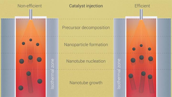
Their study in the American Chemical Society journal ACS Nano focuses on MoS2’s “pre-history,” specifically what happens in a CVD furnace once all the solid ingredients are in place. CVD, often associated with graphene and carbon nanotubes, has been exploited to make a variety of 2D materials by providing solid precursors and catalysts that sublimate into gas and react. The chemistry dictates which molecules fall out of the gas and settle on a substrate, like copper or silicone, and assemble into a 2D crystal.

The problem has been that once the furnace cranks up, it’s impossible to see or measure the complicated chain of reactions in the chemical stew in real time.

“Hundreds of labs are cooking these TMDs, quite oblivious to the intricate transformations occurring in the dark oven,” said Yakobson, the Karl F. Hasselmann Professor of Materials Science and NanoEngineering and a professor of chemistry. “Here, we’re using quantum-chemical simulations and analysis to reveal what’s there, in the dark, that leads to synthesis.”

Yakobson’s theories often lead experimentalists to make his predictions come true. (For example, boron buckyballs.) This time, the Rice lab determined the path molybdenum oxide (MoO3) and sulfur powder take to deposit an atomically thin lattice onto a surface.

The short answer is that it takes three steps. First, the solids are sublimated through heating to change them from solid to gas, including what Yakobson called a “beautiful” ring-molecule, trimolybdenum nonaoxide (Mo3O9). Second, the molybdenum-containing gases react with sulfur atoms under high heat, up to 4,040 degrees Fahrenheit. Third, molybdenum and sulfur molecules fall to the surface, where they crystallize into the jacks-like lattice that is characteristic of TMDs.

What happens in the middle step was of the most interest to the researchers. The lab’s simulations showed a trio of main gas phase reactants are the prime suspects in making MoS2: sulfur, the ring-like Mo3O9 molecules that form in sulfur’s presence and the subsequent hybrid of MoS6 that forms the crystal, releasing excess sulfur atoms in the process.

Lei said the molecular dynamics simulations showed the activation barriers that must be overcome to move the process along, usually in picoseconds.

“In our molecular dynamics simulation, we find that this ring is opened by its interaction with sulfur, which attacks oxygen connected to the molybdenum atoms,” he said. “The ring becomes a chain, and further interactions with the sulfur molecules separate this chain into molybdenum sulfide monomers. The most important part is the chain breaking, which overcomes the highest energy barrier.”

That realization could help labs streamline the process, Lei said. “If we can find precursor molecules with only one molybdenum atom, we would not need to overcome the high barrier of breaking the chain,” he said.

Yakobson said the study could apply to other TMDs.

“The findings raise oftentimes empirical nanoengineering to become a basic science-guided endeavor, where processes can be predicted and optimized,” he said, noting that while the chemistry has been generally known since the discovery of TMD fullerenes in the early ’90s, understanding the specifics will further the development of 2D synthesis.

“Only now can we ‘sequence’ the step-by-step chemistry involved,” Yakobson said. “That will allow us to improve the quality of 2D material, and also see which gas side-products might be useful and captured on the way, opening opportunities for chemical engineering.”

Here’s a link to and a citation for the paper,

Gas-Phase “Prehistory” and Molecular Precursors in Monolayer Metal Dichalcogenides Synthesis: The Case of MoS2 by Jincheng Lei, Yu Xie, and Boris I. Yakobson. ACS Nano 2021, 15, 6, 10525–10531 DOI: https://doi.org/10.1021/acsnano.1c03103 Publication Date: June 9, 2021 Copyright © 2021 American Chemical Society

This paper is behind a paywall.

Boost single-walled carbon nantube (SWCNT) production

I’m fascinated by this image,

Caption: Skoltech researchers have investigated the procedure for catalyst delivery used in the most common method of carbon nanotube production, chemical vapor deposition (CVD), offering what they call a “simple and elegant” way to boost productivity and pave the way for cheaper and more accessible nanotube-based technology. Credit: Pavel Odinev/Skoltech

If I understand it correctly, getting the catalyst particles into a tighter, more uniform formation is what could lead to a boost in the production of single-walled carbon nanotubes (SWCNTs).

The work was announced in a Nov. 30, 2020 news item in Nanowerk,

Skoltech [Skolkovo Institute of Science and Technology; Russia] researchers have investigated the procedure for catalyst delivery used in the most common method of carbon nanotube production, chemical vapor deposition (CVD), offering what they call a “simple and elegant” way to boost productivity and pave the way for cheaper and more accessible nanotube-based technology.

A Nov. 30, 2020 Skolkovo Institute of Science and Technology (Skoltech) press release (also on EurekAlert but published on Dec. 1, 2020), which originated the news item, explains in detail,

Single-walled carbon nanotubes (SWCNT), tiny rolled sheets of graphene with a thickness of just one atom, hold huge promise when it comes to applications in materials science and electronics. That is the reason why so much effort is focused on perfecting the synthesis of SWCNTs; from physical methods, such as using laser beams to ablate a graphite target, all the way to the most common CVD approach, when metal catalyst particles are used to “strip” a carbon-containing gas of its carbon and grow the nanotubes on these particles.

“The road from raw materials to carbon nanotubes requires a fine balance between dozens of reactor parameters. The formation of carbon nanotubes is a tricky and complex process that has been studied for a long time, but still keeps many secrets,” explains Albert Nasibulin, a professor at Skoltech and an adjunct professor at the Department of Chemistry and Materials Science, Aalto University School of Chemical Engineering.

Various ways of enhancing catalyst activation, in order to produce more SWCNTs with the required properties, have already been suggested. Nasibulin and his colleagues focused on the injection procedure, namely on how to distribute ferrocene vapor (a commonly used catalyst precursor) within the reactor.

They grew their carbon nanotubes using the aerosol CVD approach, using carbon monoxide as a source of carbon, and monitored the synthesis productivity and SWCNT characteristics (such as their diameter) depending on the rate of catalyst injection and the concentration of CO2 (carbon dioxide; used as an agent for fine-tuning). Ultimately the researchers concluded that “injector flow rate adjustment could lead to a 9-fold increase in the synthesis productivity while preserving most of the SWCNT characteristics”, such as their diameter, the share of defective nanotubes, and film conductivity.

“Every technology is always about efficiency. When it comes to CVD production of nanotubes, the efficiency of the catalyst is usually out of sight. However, we see a great opportunity there and this work is only a first step towards an efficient technology,” Dmitry Krasnikov, senior research scientist at Skoltech and co-author of the paper, says.

Here’s a link to and a citation for the paper,

Activation of catalyst particles for single-walled carbon nanotube synthesis by Eldar M.Khabushev, Julia V. Kolodiazhnaia, Dmitry V. Krasnikov, Albert G. Nasibulin. Chemical Engineering Journal DOI: https://doi.org/10.1016/j.cej.2020.127475 Available online 24 October 2020, 127475

This paper is behind a paywall.

Graphene-gilded artifacts (or artefacts)

Caption: L: An artist rendering of graphene gilding on Tutankhamun’s middle coffin (original photograph copyright: Griffith Institute, University of Oxford). R: Microscope image of a graphene crystal is shown on the palladium leaf. Although graphene is only a single atom thick, it can be observed in the scanning electron microscope. Here, a small crystal of graphene is shown to observe its edges. The team produces leaves where the graphene fully cover the metal surface. Credit: Original photograph copyright: Griffith Institute, University of Oxford

As icons go, Tutankhamun’s middle coffin ranks highly and it’s a great image to use as an example of what might be accomplished with graphene gilding. From a Sept. 10, 2018 news item on Nanowerk,

Gilding is the process of coating intricate artifacts with precious metals. Ancient Egyptians and Chinese coated their sculptures with thin metal films using gilding—and these golden sculptures have resisted corrosion, wear, and environmental degradation for thousands of years. The middle and outer coffins of Tutankhamun, for instance, are gold leaf gilded, as are many other ancient treasures.

In a new study, Illinois’ Sameh Tawfick, from the Department of Mechanical Science & Engineering (MechSE) and the Beckman Institute, inspired by this ancient process, has added a single layer of carbon atoms, known as graphene, on top of metal leaves—doubling the protective quality of gilding against wear and tear.

A Sept. 10, 2018 University of Illinois news release (also on EurekAlert), which originated the news item, offers more details,

Metal leaves, or foils, offer many advantages as a scalable coating material, including their commercial availability in large rolls and their comparatively low price. By bonding a single layer of graphene to the leaves, Tawfick and his team demonstrated unexpected benefits, including enhanced mechanical resistance. Their work presents exciting opportunities for protective coating applications on large structures like buildings or ship hulls, metal surfaces of consumer electronics, and small precious artifacts or jewelry.

“Adding one more layer of graphene atoms onto the palladium made it twice as resistant to indents than the bare leaves alone,” said Tawfick. “It’s also very attractive from a cost perspective. The amount of graphene needed to cover the gilded structures of the Carbide & Carbon Building in Chicago, for example, would be the size of the head of a pin.”

Additionally, the team developed a new technology to grow high-quality graphene directly on the surface of 150 nanometer-thin palladium leaves—in just 30 seconds. Using a process called chemical vapor deposition, in which the metal leaf is processed in a 1,100°C furnace, the bare palladium leaf acts as a catalyst, allowing the gases to react quickly.

“Chemical vapor deposition of graphene requires a very high temperature, which could melt the leaves or cause them to bead up by a process called solid state dewetting,” said Kaihao Zhang, PhD candidate in MechSE and lead author of the study. “The process we developed deposits the graphene quickly enough to avoid high-temperature degradation, it’s scalable, and it produces graphene of very high quality.”

Here’s a link to and a citation for the paper,

Gilding with Graphene: Rapid Chemical Vapor Deposition Synthesis of Graphene on Thin Metal Leaves by Kaihao Zhang, Charalampos Androulidakis, Mingze Chen, Sameh Tawfick. Advanced Functional Materials DOI: https://doi.org/10.1002/adfm.201804068 First published: 06 September 2018

This paper is behind  a paywall.

Scientists claim off-the-shelf, power-generating clothes almost here

PEDOT-coated yarns act as “normal” wires to transmit electricity from a wall outlet to an incandescent lightbulb. Materials scientist Trisha Andrew at UMass Amherst and colleagues outline in a new paper how they have invented a way to apply breathable, pliable, metal-free electrodes to fabric and off-the-shelf clothing so it feels good to the touch and also transports electricity to power small electronics. Harvesting body motion energy generates the power. Courtesy: UMass Amherst

I’m not quite as optimistic (it’s a long way from the lab to the marketplace) as the scientists do eventually note but this does seem promising (from a May 23, 2017 news item on Nanowerk),

A lightweight, comfortable jacket that can generate the power to light up a jogger at night may sound futuristic, but materials scientist Trisha Andrew at the University of Massachusetts Amherst could make one today.

In a new paper this month, she and colleagues outline how they have invented a way to apply breathable, pliable, metal-free electrodes to fabric and off-the-shelf clothing so it feels good to the touch and also transports enough electricity to power small electronics.

A May 23, 2017 University of Massachusetts Amherst news release (also on EurekAlert), which originated the news item,

She says, “Our lab works on textile electronics. We aim to build up the materials science so you can give us any garment you want, any fabric, any weave type, and turn it into a conductor. Such conducting textiles can then be built up into sophisticated electronics. One such application is to harvest body motion energy and convert it into electricity in such a way that every time you move, it generates power.” Powering advanced fabrics that can monitor health data remotely are important to the military and increasingly valued by the health care industry, she notes.

Generating small electric currents through relative movement of layers is called triboelectric charging, explains Andrew, who trained as a polymer chemist and electrical engineer. Materials can become electrically charged as they create friction by moving against a different material, like rubbing a comb on a sweater. “By sandwiching layers of differently materials between two conducting electrodes, a few microwatts of power can be generated when we move,” she adds.

In the current early online edition of Advanced Functional Materials, she and postdoctoral researcher Lu Shuai Zhang in her lab describe the vapor deposition method they use to coat fabrics with a conducting polymer, poly(3,4-ethylenedioxytiophene) also known as PEDOT, to make plain-woven, conducting fabrics that are resistant to stretching and wear and remain stable after washing and ironing. The thickest coating they put down is about 500 nanometers, or about 1/10 the diameter of a human hair, which retains a fabric’s hand feel.

The authors report results of testing electrical conductivity, fabric stability, chemical and mechanical stability of PEDOT films and textile parameter effects on conductivity for 14 fabrics, including five cottons with different weaves, linen and silk from a craft store.

“Our article describes the materials science needed to make these robust conductors,” Andrew says. “We show them to be stable to washing, rubbing, human sweat and a lot of wear and tear.” PEDOT coating did not change the feel of any fabric as determined by touch with bare hands before and after coating. Coating did not increase fabric weight by more than 2 percent. The work was supported by the Air Force Office of Scientific Research.

Until recently, she and Zhang point out, textile scientists have tended not to use vapor deposition because of technical difficulties and high cost of scaling up from the laboratory. But over the last 10 years, industries such as carpet manufacturers and mechanical component makers have shown that the technology can be scaled up and remain cost-effective. The researchers say their invention also overcomes the obstacle of power-generating electronics mounted on plastic or cladded, veneer-like fibers that make garments heavier and/or less flexible than off-the-shelf clothing “no matter how thin or flexible these device arrays are.”

“There is strong motivation to use something that is already familiar, such as cotton/silk thread, fabrics and clothes, and imperceptibly adapting it to a new technological application.” Andrew adds, “This is a huge leap for consumer products, if you don’t have to convince people to wear something different than what they are already wearing.”

Test results were sometimes a surprise, Andrew notes. “You’d be amazed how much stress your clothes go through until you try to make a coating that will survive a shirt being pulled over the head. The stress can be huge, up to a thousand newtons of force. For comparison, one footstep is equal to about 10 newtons, so it’s yanking hard. If your coating is not stable, a single pull like that will flake it all off. That’s why we had to show that we could bend it, rub it and torture it. That is a very powerful requirement to move forward.”

Andrew is director of wearable electronics at the Center for Personalized Health Monitoring in UMass Amherst’s Institute of Applied Life Sciences (IALS). Since the basic work reported this month was completed, her lab has also made a wearable heart rate monitor with an off-the-shelf fitness bra to which they added eight monitoring electrodes. They will soon test it with volunteers on a treadmill at the IALS human movement facility.

She explains that a hospital heart rate monitor has 12 electrodes, while the wrist-worn fitness devices popular today have one, which makes them prone to false positives. They will be testing a bra with eight electrodes, alone and worn with leggings that add four more, against a control to see if sensors can match the accuracy and sensitivity of what a hospital can do. As the authors note in their paper, flexible, body-worn electronics represent a frontier of human interface devices that make advanced physiological and performance monitoring possible.

For the future, Andrew says, “We’re working on taking any garment you give us and turning it into a solar cell so that as you are walking around the sunlight that hits your clothes can be stored in a battery or be plugged in to power a small electronic device.”

Zhang and Andrew believe their vapor coating is able to stick to fabrics by a process called surface grafting, which takes advantage of free bonds dangling on the surface chemically bonding to one end of the polymer coating, but they have yet to investigate this fully.

Here’s a link to and a citation for the paper,

Rugged Textile Electrodes for Wearable Devices Obtained by Vapor Coating Off-the-Shelf, Plain-Woven Fabrics by Lushuai Zhang, Marianne Fairbanks, and Trisha L. Andrew. Advanced Functional Materials DOI: 10.1002/adfm.201700415 Version of Record online: 2 MAY 2017

© 2017 WILEY-VCH Verlag GmbH & Co. KGaA, Weinheim

This paper is behind a paywall.

Serendipity and coaxial nanocables

I like the sound of the word coaxial especially when it’s used in conjunction with cable, as in coaxial cable. Adding the world serendipity to the mix, as they did at Rice University, made the June 7, 2012 news item by Jade Boyd on the Nanowerk website irresistible [Note: I have removed a link.],

Thanks to a little serendipity, researchers at Rice University have created a tiny coaxial cable that is about a thousand times smaller than a human hair and has higher capacitance than previously reported microcapacitors.

The nanocable, which is described this week in Nature Communications (“Anomalous high capacitance in a coaxial single nanowire capacitor” [behind paywall]), was produced with techniques pioneered in the nascent graphene research field and could be used to build next-generation energy-storage systems. It could also find use in wiring up components of lab-on-a-chip processors, but its discovery is owed partly to chance.

“We didn’t expect to create this when we started,” said study co-author Jun Lou, associate professor of mechanical engineering and materials science at Rice. “At the outset, we were just curious to see what would happen electrically and mechanically if we took small copper wires known as interconnects and covered them with a thin layer of carbon.”

Boyd’s June 7, 2012 news item can also be read in its entirety at the Rice University website [Note: I have removed some links.],

The tiny coaxial cable is remarkably similar in makeup to the ones that carry cable television signals into millions of homes and offices. The heart of the cable is a solid copper wire that is surrounded by a thin sheath of insulating copper oxide. A third layer, another conductor, surrounds that. In the case of TV cables, the third layer is copper again, but in the nanocable it is a thin layer of carbon measuring just a few atoms thick. The coax nanocable is about 100 nanometers, or 100 billionths of a meter, wide.

While the coaxial cable is a mainstay of broadband telecommunications, the three-layer, metal-insulator-metal structure can also be used to build energy-storage devices called capacitors. Unlike batteries, which rely on chemical reactions to both store and supply electricity, capacitors use electrical fields. A capacitor contains two electrical conductors, one negative and the other positive, that are separated by thin layer of insulation. Separating the oppositely charged conductors creates an electrical potential, and that potential increases as the separated charges increase and as the distance between them – occupied by the insulating layer — decreases. The proportion between the charge density and the separating distance is known as capacitance, and it’s the standard measure of efficiency of a capacitor.

The study reports that the capacitance of the nanocable is at least 10 times greater than what would be predicted with classical electrostatics.

“The increase is most likely due to quantum effects that arise because of the small size of the cable,” said study co-author Pulickel Ajayan, Rice’s Benjamin M. and Mary Greenwood Anderson Professor of Mechanical Engineering and Materials Science.

When the project began 18 months ago, Rice postdoctoral researcher Zheng Liu, the lead co-author of the study, intended to make pure copper wires covered with carbon. The techniques for making the wires, which are just a few nanometers wide, are well-established because the wires are often used as “interconnects” in state-of-the-art electronics. Liu used a technique known as chemical vapor deposition (CVD) to cover the wires with a thin coating of carbon. The CVD technique is also used to grow sheets of single-atom-thick carbon called graphene on films of copper.

“When people make graphene, they usually want to study the graphene and they aren’t very interested in the copper,” Lou said. “It’s just used a platform for making the graphene.”

When Liu ran some electronic tests on his first few samples, the results were far from what he expected.

“We eventually found that a thin layer of copper oxide — which is served as a dielectric layer — was forming between the copper and the carbon,” said Liu.

Here’s an image illustrating this process,

The three-layer coaxial nanocable contains a solid copper wire surrounded by a layer of copper oxide that is encased a layer of carbon just a few atoms thick. (Courtesy: Rice University)

The researchers don’t seem to have any particular applications in mind for their nancoaxial cable although they seem hopeful about a few possibilities (from the June 7, 2012 news item on the Rice University website,

The capacitance of the new nanocable is up to 143 microfarads per centimeter squared, better than the best previous results from microcapacitors.

Lou said it may be possible to build a large-scale energy-storage device by arranging millions of the tiny nanocables side by side in large arrays.

“The nanoscale cable might also be used as a transmission line for radio frequency signals at the nanoscale,” Liu said. “This could be useful as a fundamental building block in micro- and nano-sized electromechanical systems like lab-on-a-chip devices.”

Who knows where serendipity will take this discovery?

As for why that word made the item irresistible to me, many years ago I was at a dinner party and one of the guests (a vivid storyteller and born in Sri Lanka) explained the origin of the word, serendipity. Sadly I don’t remember the details of her story, so here’s a less rich version of the story from the Encyclopedia Britannia website,

Serendib, also spelled Serendip, Arabic Sarandīb, name for the island of Sri Lanka (Ceylon). The name, Arabic in origin, was recorded in use at least as early as ad 361 and for a time gained considerable currency in the West. It is best known to speakers of English through the word serendipity, invented in the 18th century by the English man of letters Horace Walpole on the inspiration of a Persian fairy tale, “The Three Princes of Serendip,” whose heroes often made discoveries by chance.