Tag Archives: Chi Hwan Lee

Spider web-like electronics with graphene

A spiderweb-inspired fractal design is used for hemispherical 3D photodetection to replicate the vision system of arthropods. (Sena Huh image)

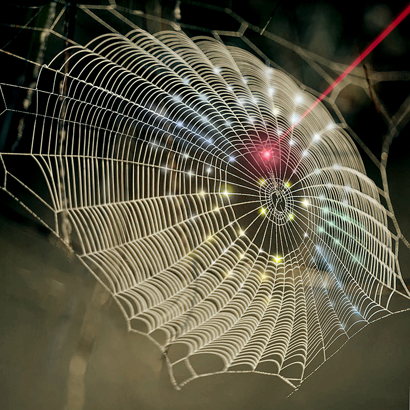
This image is pretty and I’m pretty sure it’s an illustration and not a real photodetection system. Regardless, an Oct. 21, 2020 news item on Nanowerk describes the research into producing a real 3D hemispheric photodetector for biomedical imaging (Note: A link has been removed),

Purdue University innovators are taking cues from nature to develop 3D photodetectors for biomedical imaging.

The researchers used some architectural features from spider webs to develop the technology. Spider webs typically provide excellent mechanical adaptability and damage-tolerance against various mechanical loads such as storms.

“We employed the unique fractal design of a spider web for the development of deformable and reliable electronics that can seamlessly interface with any 3D curvilinear surface,” said Chi Hwan Lee, a Purdue assistant professor of biomedical engineering and mechanical engineering. “For example, we demonstrated a hemispherical, or dome-shaped, photodetector array that can detect both direction and intensity of incident light at the same time, like the vision system of arthropods such as insects and crustaceans.”

The Purdue technology uses the structural architecture of a spider web that exhibits a repeating pattern. This work is published in Advanced Materials (“Fractal Web Design of a Hemispherical Photodetector Array with Organic-Dye-Sensitized Graphene Hybrid Composites”).

An Oct. 21, 2020 Purdue University news release by Chris Adam, which originated the news item, delves further into the work,

Lee said this provides unique capabilities to distribute externally induced stress throughout the threads according to the effective ratio of spiral and radial dimensions and provides greater extensibility to better dissipate force under stretching. Lee said it also can tolerate minor cuts of the threads while maintaining overall strength and function of the entire web architecture.

“The resulting 3D optoelectronic architectures are particularly attractive for photodetection systems that require a large field of view and wide-angle antireflection, which will be useful for many biomedical and military imaging purposes,” said Muhammad Ashraful Alam, the Jai N. Gupta Professor of Electrical and Computer Engineering.

Alam said the work establishes a platform technology that can integrate a fractal web design with system-level hemispherical electronics and sensors, thereby offering several excellent mechanical adaptability and damage-tolerance against various mechanical loads.

“The assembly technique presented in this work enables deploying 2D deformable electronics in 3D architectures, which may foreshadow new opportunities to better advance the field of 3D electronic and optoelectronic devices,” Lee said.

Here’s a link to and a citation for the paper,

Fractal Web Design of a Hemispherical Photodetector Array with Organic‐Dye‐Sensitized Graphene Hybrid Composites by Eun Kwang Lee, Ratul Kumar Baruah, Jung Woo Leem, Woohyun Park, Bong Hoon Kim, Augustine Urbas, Zahyun Ku, Young L. Kim, Muhammad Ashraful Alam, Chi Hwan Lee. Advanced Materials Volume 32, Issue 46 November 19, 2020 2004456 DOI: https://doi.org/10.1002/adma.202004456 First published online: 12 October 2020

This paper is behind a paywall.

Thin-film electronic stickers for the Internet of Things (IoT)

This research is from Purdue University (Indiana, US) and the University of Virginia (US) increases and improves the interactivity between objects in what’s called the Internet of Things (IoT).

Caption: Electronic stickers can turn ordinary toy blocks into high-tech sensors within the ‘internet of things.’ Credit: Purdue University image/Chi Hwan Lee

From a July 16, 2018 news item on ScienceDaily,

Billions of objects ranging from smartphones and watches to buildings, machine parts and medical devices have become wireless sensors of their environments, expanding a network called the “internet of things.”

As society moves toward connecting all objects to the internet — even furniture and office supplies — the technology that enables these objects to communicate and sense each other will need to scale up.

Researchers at Purdue University and the University of Virginia have developed a new fabrication method that makes tiny, thin-film electronic circuits peelable from a surface. The technique not only eliminates several manufacturing steps and the associated costs, but also allows any object to sense its environment or be controlled through the application of a high-tech sticker.

Eventually, these stickers could also facilitate wireless communication. …

A July 16, 2018 University of Purdue news release (also on EurekAlert), which originated the news item, explains more,

“We could customize a sensor, stick it onto a drone, and send the drone to dangerous areas to detect gas leaks, for example,” said Chi Hwan Lee, Purdue assistant professor of biomedical engineering and mechanical engineering.

Most of today’s electronic circuits are individually built on their own silicon “wafer,” a flat and rigid substrate. The silicon wafer can then withstand the high temperatures and chemical etching that are used to remove the circuits from the wafer.

But high temperatures and etching damage the silicon wafer, forcing the manufacturing process to accommodate an entirely new wafer each time.

Lee’s new fabrication technique, called “transfer printing,” cuts down manufacturing costs by using a single wafer to build a nearly infinite number of thin films holding electronic circuits. Instead of high temperatures and chemicals, the film can peel off at room temperature with the energy-saving help of simply water.

“It’s like the red paint on San Francisco’s Golden Gate Bridge – paint peels because the environment is very wet,” Lee said. “So in our case, submerging the wafer and completed circuit in water significantly reduces the mechanical peeling stress and is environmentally-friendly.”

A ductile metal layer, such as nickel, inserted between the electronic film and the silicon wafer, makes the peeling possible in water. These thin-film electronics can then be trimmed and pasted onto any surface, granting that object electronic features.

Putting one of the stickers on a flower pot, for example, made that flower pot capable of sensing temperature changes that could affect the plant’s growth.

Lee’s lab also demonstrated that the components of electronic integrated circuits work just as well before and after they were made into a thin film peeled from a silicon wafer. The researchers used one film to turn on and off an LED light display.

“We’ve optimized this process so that we can delaminate electronic films from wafers in a defect-free manner,” Lee said.

This technology holds a non-provisional U.S. patent. The work was supported by the Purdue Research Foundation, the Air Force Research Laboratory (AFRL-S-114-054-002), the National Science Foundation (NSF-CMMI-1728149) and the University of Virginia.

The researchers have provided a video,

Here’s a link to and a citation for the paper,

Wafer-recyclable, environment-friendly transfer printing for large-scale thin-film nanoelectronics by Dae Seung Wie, Yue Zhang, Min Ku Kim, Bongjoong Kim, Sangwook Park, Young-Joon Kim, Pedro P. Irazoqui, Xiaolin Zheng, Baoxing Xu, and Chi Hwan Lee.
PNAS July 16, 2018 201806640 DOI: https://doi.org/10.1073/pnas.1806640115
published ahead of print July 16, 2018

This paper is behind a paywall.

Dexter Johnson provides some context in his July 25, 2018 posting on the Nanoclast blog (on the IEEE [Institute of Electronic and Electrical Engineers] website), Note: A link has been removed,

The Internet of Things (IoT), the interconnection of billions of objects and devices that will be communicating with each other, has been the topic of many futurists’ projections. However, getting the engineering sorted out with the aim of fully realizing the myriad visions for IoT is another story. One key issue to address: How do you get the electronics onto these devices efficiently and economically?

A team of researchers from Purdue University and the University of Virginia has developed a new manufacturing process that could make equipping a device with all the sensors and other electronics that will make it Internet capable as easily as putting a piece of tape on it.

… this new approach makes use of a water environment at room temperature to control the interfacial debonding process. This allows clean, intact delamination of prefabricated thin film devices when they’re pulled away from the original wafer.

The use of mechanical peeling in water rather than etching solution provides a number of benefits in the manufacturing scheme. Among them are simplicity, controllability, and cost effectiveness, says Chi Hwan Lee, assistant professor at Purdue University and coauthor of the paper chronicling the research.

If you have the time, do read Dexter’s piece. He always adds something that seems obvious in retrospect but wasn’t until he wrote it.

Skin-like electronic bandage

Not sure how I feel about an electronic bandage, presumably it won’t electrocute me should it encounter my blood. If the Nov. 17, 2016 news item on phys.org is to be believed, it’s more sensor than bandage,

A skin-like biomedical technology that uses a mesh of conducting nanowires and a thin layer of elastic polymer might bring new electronic bandages that monitor biosignals for medical applications and provide therapeutic stimulation through the skin.

The biomedical device mimics the human skin’s elastic properties and sensory capabilities.

“It can intimately adhere to the skin and simultaneously provide medically useful biofeedback such as electrophysiological signals,” said Chi Hwan Lee, an assistant professor of biomedical engineering and mechanical engineering at Purdue University. “Uniquely, this work combines high-quality nanomaterials into a skin-like device, thereby enhancing the mechanical properties.”

The device could be likened to an electronic bandage and might be used to treat medical conditions using thermotherapeutics, where heat is applied to promote vascular flow for enhanced healing, said Lee, who worked with a team that includes Purdue graduate student Min Ku Kim.

A November 17, 2016 Purdue University news release by Emil Venere, which originated the news item, provides more insight into the work,

Traditional approaches to developing such a technology have used thin films made of ductile metals such as gold, silver and copper.

“The problem is that these thin films are susceptible to fractures by over-stretching and cracking,” Lee said. “Instead of thin films we use nanowire mesh film, which makes the device more resistive to stretching and cracking than otherwise possible. In addition, the nanowire mesh film has very high surface area compared to conventional thin films, with more than 1,000 times greater surface roughness. So once you attach it to the skin the adhesion is much higher, reducing the potential of inadvertent delamination.”

Findings are detailed in a research publication appearing online in October [2016] in Advanced Materials. The paper is also available online at http://onlinelibrary.wiley.com/doi/10.1002/adma.201603878/full and was authored by Kim; postdoctoral researcher Seungyong Han at the University of Illinois, Urbana-Champaign; Purdue graduate student Dae Seung Wie; Oklahoma State University assistant professor Shuodao Wang and postdoctoral researcher Bo Wang; and Lee.

The conducting nanowires are around 50 nanometers in diameter and more than 150 microns long and are embedded inside a thin layer of elastomer, or elastic polymer, about 1.5 microns thick. To demonstrate its utility in medical diagnostics, the device was used to record electrophysiological signals from the heart and muscles. A YouTube video about the research is available at https://youtu.be/tYRebHNi6p4.

“Recording the electrophysiological signals from the skin can provide wearers and clinicians with quantitative measures of the heart’s activity or the muscle’s activity,” Lee said.

Much of the research was performed in the Birck Nanotechnology Center in Purdue’s Discovery Park.

“The nanowires mesh film was initially formed on a conventional silicon wafer with existing micro- and nano-fabrication technologies. Our unique technique, called a crack-driven transfer printing technique, allows us to controllably peel off the device layer from the silicon wafer, and then apply onto the skin,” Lee said.

The Oklahoma State researchers contributed theoretical simulations related to the underlying mechanics of the devices, and Seungyong Han synthesized and provided the conducting nanowires.

Future research will be dedicated to developing a transdermal drug-delivery bandage that would transport medications through the skin in an electronically controlled fashion. Such a system might include built-in sensors to detect the level of injury and autonomously deliver the appropriate dose of drugs.

Here’s a link to and a citation for the paper mentioned in the news release,

Mechanically Reinforced Skin-Electronics with Networked Nanocomposite Elastomer by Seungyong Han, Min Ku Kim, Bo Wang, Dae Seung Wie, Shuodao Wang, and Chi Hwan Lee. Advanced Materials DOI: 10.1002/adma.201603878 Version of Record online: 7 OCT 2016

© 2016 WILEY-VCH Verlag GmbH & Co. KGaA, Weinheim

This paper is behind a paywall but you can watch the video mentioned in the news release,

It seems that liquids won’t be a problem with regard to electrocution and I notice they keep calling it a biopatch not a bandaid.