Tag Archives: computer chips

Combining silicon with metal oxide memristors to create powerful, low-energy intensive chips enabling AI in portable devices

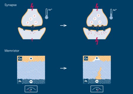
In this one week, I’m publishing my first stories (see also June 13, 2023 posting “ChatGPT and a neuromorphic [brainlike] synapse“) where artificial intelligence (AI) software is combined with a memristor (hardware component) for brainlike (neuromorphic) computing.

Here’s more about some of the latest research from a March 30, 2023 news item on ScienceDaily,

Everyone is talking about the newest AI and the power of neural networks, forgetting that software is limited by the hardware on which it runs. But it is hardware, says USC [University of Southern California] Professor of Electrical and Computer Engineering Joshua Yang, that has become “the bottleneck.” Now, Yang’s new research with collaborators might change that. They believe that they have developed a new type of chip with the best memory of any chip thus far for edge AI (AI in portable devices).

A March 29, 2023 University of Southern California (USC) news release (also on EurekAlert), which originated the news item, contextualizes the research and delves further into the topic of neuromorphic hardware,

For approximately the past 30 years, while the size of the neural networks needed for AI and data science applications doubled every 3.5 months, the hardware capability needed to process them doubled only every 3.5 years. According to Yang, hardware presents a more and more severe problem for which few have patience. 

Governments, industry, and academia are trying to address this hardware challenge worldwide. Some continue to work on hardware solutions with silicon chips, while others are experimenting with new types of materials and devices.  Yang’s work falls into the middle—focusing on exploiting and combining the advantages of the new materials and traditional silicon technology that could support heavy AI and data science computation. 

Their new paper in Nature focuses on the understanding of fundamental physics that leads to a drastic increase in memory capacity needed for AI hardware. The team led by Yang, with researchers from USC (including Han Wang’s group), MIT [Massachusetts Institute of Technology], and the University of Massachusetts, developed a protocol for devices to reduce “noise” and demonstrated the practicality of using this protocol in integrated chips. This demonstration was made at TetraMem, a startup company co-founded by Yang and his co-authors  (Miao Hu, Qiangfei Xia, and Glenn Ge), to commercialize AI acceleration technology. According to Yang, this new memory chip has the highest information density per device (11 bits) among all types of known memory technologies thus far. Such small but powerful devices could play a critical role in bringing incredible power to the devices in our pockets. The chips are not just for memory but also for the processor. And millions of them in a small chip, working in parallel to rapidly run your AI tasks, could only require a small battery to power it. 

The chips that Yang and his colleagues are creating combine silicon with metal oxide memristors in order to create powerful but low-energy intensive chips. The technique focuses on using the positions of atoms to represent information rather than the number of electrons (which is the current technique involved in computations on chips). The positions of the atoms offer a compact and stable way to store more information in an analog, instead of digital fashion. Moreover, the information can be processed where it is stored instead of being sent to one of the few dedicated ‘processors,’ eliminating the so-called ‘von Neumann bottleneck’ existing in current computing systems.  In this way, says Yang, computing for AI is “more energy efficient with a higher throughput.”

How it works: 

Yang explains that electrons which are manipulated in traditional chips, are “light.” And this lightness, makes them prone to moving around and being more volatile.  Instead of storing memory through electrons, Yang and collaborators are storing memory in full atoms. Here is why this memory matters. Normally, says Yang, when one turns off a computer, the information memory is gone—but if you need that memory to run a new computation and your computer needs the information all over again, you have lost both time and energy.  This new method, focusing on activating atoms rather than electrons, does not require battery power to maintain stored information. Similar scenarios happen in AI computations, where a stable memory capable of high information density is crucial. Yang imagines this new tech that may enable powerful AI capability in edge devices, such as Google Glasses, which he says previously suffered from a frequent recharging issue.

Further, by converting chips to rely on atoms as opposed to electrons, chips become smaller.  Yang adds that with this new method, there is more computing capacity at a smaller scale. And this method, he says, could offer “many more levels of memory to help increase information density.” 

To put it in context, right now, ChatGPT is running on a cloud. The new innovation, followed by some further development, could put the power of a mini version of ChatGPT in everyone’s personal device. It could make such high-powered tech more affordable and accessible for all sorts of applications. 

Here’s a link to and a citation for the paper,

Thousands of conductance levels in memristors integrated on CMOS by Mingyi Rao, Hao Tang, Jiangbin Wu, Wenhao Song, Max Zhang, Wenbo Yin, Ye Zhuo, Fatemeh Kiani, Benjamin Chen, Xiangqi Jiang, Hefei Liu, Hung-Yu Chen, Rivu Midya, Fan Ye, Hao Jiang, Zhongrui Wang, Mingche Wu, Miao Hu, Han Wang, Qiangfei Xia, Ning Ge, Ju Li & J. Joshua Yang. Nature volume 615, pages 823–829 (2023) DOI: https://doi.org/10.1038/s41586-023-05759-5 Issue Date: 30 March 2023 Published: 29 March 2023

This paper is behind a paywall.

New design directions to increase variety, efficiency, selectivity and reliability for memristive devices

A May 11, 2020 news item on ScienceDaily provides a description of the current ‘memristor scene’ along with an announcement about a piece of recent research,

Scientists around the world are intensively working on memristive devices, which are capable in extremely low power operation and behave similarly to neurons in the brain. Researchers from the Jülich Aachen Research Alliance (JARA) and the German technology group Heraeus have now discovered how to systematically control the functional behaviour of these elements. The smallest differences in material composition are found crucial: differences so small that until now experts had failed to notice them. The researchers’ design directions could help to increase variety, efficiency, selectivity and reliability for memristive technology-based applications, for example for energy-efficient, non-volatile storage devices or neuro-inspired computers.

Memristors are considered a highly promising alternative to conventional nanoelectronic elements in computer Chips [sic]. Because of the advantageous functionalities, their development is being eagerly pursued by many companies and research institutions around the world. The Japanese corporation NEC installed already the first prototypes in space satellites back in 2017. Many other leading companies such as Hewlett Packard, Intel, IBM, and Samsung are working to bring innovative types of computer and storage devices based on memristive elements to market.

Fundamentally, memristors are simply “resistors with memory,” in which high resistance can be switched to low resistance and back again. This means in principle that the devices are adaptive, similar to a synapse in a biological nervous system. “Memristive elements are considered ideal candidates for neuro-inspired computers modelled on the brain, which are attracting a great deal of interest in connection with deep learning and artificial intelligence,” says Dr. Ilia Valov of the Peter Grünberg Institute (PGI-7) at Forschungszentrum Jülich.

In the latest issue of the open access journal Science Advances, he and his team describe how the switching and neuromorphic behaviour of memristive elements can be selectively controlled. According to their findings, the crucial factor is the purity of the switching oxide layer. “Depending on whether you use a material that is 99.999999 % pure, and whether you introduce one foreign atom into ten million atoms of pure material or into one hundred atoms, the properties of the memristive elements vary substantially” says Valov.

A May 11, 2020 Forschungszentrum Juelich press release (also on EurekAlert), which originated the news item, delves into the theme of increasing control over memristive systems,

This effect had so far been overlooked by experts. It can be used very specifically for designing memristive systems, in a similar way to doping semiconductors in information technology. “The introduction of foreign atoms allows us to control the solubility and transport properties of the thin oxide layers,” explains Dr. Christian Neumann of the technology group Heraeus. He has been contributing his materials expertise to the project ever since the initial idea was conceived in 2015.

“In recent years there has been remarkable progress in the development and use of memristive devices, however that progress has often been achieved on a purely empirical basis,” according to Valov. Using the insights that his team has gained, manufacturers could now methodically develop memristive elements selecting the functions they need. The higher the doping concentration, the slower the resistance of the elements changes as the number of incoming voltage pulses increases and decreases, and the more stable the resistance remains. “This means that we have found a way for designing types of artificial synapses with differing excitability,” explains Valov.

Design specification for artificial synapses

The brain’s ability to learn and retain information can largely be attributed to the fact that the connections between neurons are strengthened when they are frequently used. Memristive devices, of which there are different types such as electrochemical metallization cells (ECMs) or valence change memory cells (VCMs), behave similarly. When these components are used, the conductivity increases as the number of incoming voltage pulses increases. The changes can also be reversed by applying voltage pulses of the opposite polarity.

The JARA researchers conducted their systematic experiments on ECMs, which consist of a copper electrode, a platinum electrode, and a layer of silicon dioxide between them. Thanks to the cooperation with Heraeus researchers, the JARA scientists had access to different types of silicon dioxide: one with a purity of 99.999999 % – also called 8N silicon dioxide – and others containing 100 to 10,000 ppm (parts per million) of foreign atoms. The precisely doped glass used in their experiments was specially developed and manufactured by quartz glass specialist Heraeus Conamic, which also holds the patent for the procedure. Copper and protons acted as mobile doping agents, while aluminium and gallium were used as non-volatile doping.

Synapses, the connections between neurons, have the ability to transmit signals with varying degrees of strength when they are excited by a quick succession of electrical impulses. One effect of this repeated activity is to increase the concentration of calcium ions, with the result that more neurotransmitters are emitted. Depending on the activity, other effects cause long-term structural changes, which impact the strength of the transmission for several hours, or potentially even for the rest of the person’s life. Memristive elements allow the strength of the electrical transmission to be changed in a similar way to synaptic connections, by applying a voltage. In electrochemical metallization cells (ECMs), a metallic filament develops between the two metal electrodes, thus increasing conductivity. Applying voltage pulses with reversed polarity causes the filament to shrink again until the cell reaches its initial high resistance state. Copyright: Forschungszentrum Jülich / Tobias Schlößer

Record switching time confirms theory

Based on their series of experiments, the researchers were able to show that the ECMs’ switching times change as the amount of doping atoms changes. If the switching layer is made of 8N silicon dioxide, the memristive component switches in only 1.4 nanoseconds. To date, the fastest value ever measured for ECMs had been around 10 nanoseconds. By doping the oxide layer of the components with up to 10,000 ppm of foreign atoms, the switching time was prolonged into the range of milliseconds. “We can also theoretically explain our results. This is helping us to understand the physico-chemical processes on the nanoscale and apply this knowledge in the practice” says Valov. Based on generally applicable theoretical considerations, supported by experimental results, some also documented in the literature, he is convinced that the doping/impurity effect occurs and can be employed in all types memristive elements.

Top: In memristive elements (ECMs) with an undoped, high-purity switching layer of silicon oxide (SiO2), copper ions can move very fast. A filament of copper atoms forms correspondingly fast on the platinum electrode. This increases the total device conductivity respectively the capacity. Due to the high mobility of the ions, however, this filament is unstable at low forming voltages. Center: Gallium ions (Ga3+), which are introduced into the cell (non-volatile doping), bind copper ions (Cu2+) in the switching layer. The movement of the ions slows down, leading to lower switching times, but the filament, once formed remains longer stable. Bottom: Doping with aluminium ions (Al3+) slows down the process even more, since aluminium ions bind copper ions even stronger than gallium ions. Filament growth is even slower, while at the same time the stability of the filament is further increased. Depending on the chemical properties of the introduced doping elements, memristive cells – the artificial synapses – can be created with tailor-made switching and neuromorphic properties. Copyright: Forschungszentrum Jülich / Tobias Schloesser

Here’s a link to and a citation for the paper,

Design of defect-chemical properties and device performance in memristive systems by M. Lübben, F. Cüppers, J. Mohr, M. von Witzleben, U. Breuer, R. Waser, C. Neumann, and I. Valov. Science Advances 08 May 2020: Vol. 6, no. 19, eaaz9079 DOI: 10.1126/sciadv.aaz9079

This paper is open access.

For anyone curious about the German technology group, Heraeus, there’s a fascinating history in its Wikipedia entry. The technology company was formally founded in 1851 but it can be traced back to the 17th century and the founding family’s apothecary.

7nm (nanometre) chip shakeup

From time to time I check out the latest on attempts to shrink computer chips. In my July 11, 2014 posting I noted IBM’s announcement about developing a 7nm computer chip and later in my July 15, 2015 posting I noted IBM’s announcement of a working 7nm chip (from a July 9, 2015 IBM news release , “The breakthrough, accomplished in partnership with GLOBALFOUNDRIES and Samsung at SUNY Polytechnic Institute’s Colleges of Nanoscale Science and Engineering (SUNY Poly CNSE), could result in the ability to place more than 20 billion tiny switches — transistors — on the fingernail-sized chips that power everything from smartphones to spacecraft.”

I’m not sure what happened to the IBM/Global Foundries/Samsung partnership but Global Foundries recently announced that it will no longer be working on 7nm chips. From an August 27, 2018 Global Foundries news release,

GLOBALFOUNDRIES [GF] today announced an important step in its transformation, continuing the trajectory launched with the appointment of Tom Caulfield as CEO earlier this year. In line with the strategic direction Caulfield has articulated, GF is reshaping its technology portfolio to intensify its focus on delivering truly differentiated offerings for clients in high-growth markets.

GF is realigning its leading-edge FinFET roadmap to serve the next wave of clients that will adopt the technology in the coming years. The company will shift development resources to make its 14/12nm FinFET platform more relevant to these clients, delivering a range of innovative IP and features including RF, embedded memory, low power and more. To support this transition, GF is putting its 7nm FinFET program on hold indefinitely [emphasis mine] and restructuring its research and development teams to support its enhanced portfolio initiatives. This will require a workforce reduction, however a significant number of top technologists will be redeployed on 14/12nm FinFET derivatives and other differentiated offerings.

I tried to find a definition for FinFet but the reference to a MOSFET and in-gate transistors was too much incomprehensible information packed into a tight space, see the FinFET Wikipedia entry for more, if you dare.

Getting back to the 7nm chip issue, Samuel K. Moore (I don’t think he’s related to the Moore of Moore’s law) wrote an Aug. 28, 2018 posting on the Nanoclast blog (on the IEEE [Institute of Electronics and Electrical Engineers] website) which provides some insight (Note: Links have been removed),

In a major shift in strategy, GlobalFoundries is halting its development of next-generation chipmaking processes. It had planned to move to the so-called 7-nm node, then begin to use extreme-ultraviolet lithography (EUV) to make that process cheaper. From there, it planned to develop even more advanced lithography that would allow for 5- and 3-nanometer nodes. Despite having installed at least one EUV machine at its Fab 8 facility in Malta, N.Y., all those plans are now on indefinite hold, the company announced Monday.

The move leaves only three companies reaching for the highest rungs of the Moore’s Law ladder: Intel, Samsung, and TSMC.

It’s a huge turnabout for GlobalFoundries. …

GlobalFoundries rationale for the move is that there are not enough customers that need bleeding-edge 7-nm processes to make it profitable. “While the leading edge gets most of the headlines, fewer customers can afford the transition to 7 nm and finer geometries,” said Samuel Wang, research vice president at Gartner, in a GlobalFoundries press release.

“The vast majority of today’s fabless [emphasis mine] customers are looking to get more value out of each technology generation to leverage the substantial investments required to design into each technology node,” explained GlobalFoundries CEO Tom Caulfield in a press release. “Essentially, these nodes are transitioning to design platforms serving multiple waves of applications, giving each node greater longevity. This industry dynamic has resulted in fewer fabless clients designing into the outer limits of Moore’s Law. We are shifting our resources and focus by doubling down on our investments in differentiated technologies across our entire portfolio that are most relevant to our clients in growing market segments.”

(The dynamic Caulfield describes is something the U.S. Defense Advanced Research Agency is working to disrupt with its $1.5-billion Electronics Resurgence Initiative. Darpa’s [DARPA] partners are trying to collapse the cost of design and allow older process nodes to keep improving by using 3D technology.)

Fabless manufacturing is where the fabrication is outsourced and the manufacturing company of record is focused on other matters according to the Fabless manufacturing Wikipedia entry.

Roland Moore-Colyer (I don’t think he’s related to Moore of Moore’s law either) has written August 28, 2018 article for theinquirer.net which also explores this latest news from Global Foundries (Note: Links have been removed),

EVER PREPPED A SPREAD for a party to then have less than half the people you were expecting show up? That’s probably how GlobalFoundries [sic] feels at the moment.

The chip manufacturer, which was once part of AMD, had a fabrication process geared up for 7-nanometre chips which its customers – including AMD and Qualcomm – were expected to adopt.

But AMD has confirmed that it’s decided to move its 7nm GPU production to TSMC, and Intel is still stuck trying to make chips based on 10nm fabrication.

Arguably, this could mark a stymieing of innovation and cutting-edge designs for chips in the near future. But with processors like AMD’s Threadripper 2990WX overclocked to run at 6GHz across all its 32 cores, in the real-world PC fans have no need to worry about consumer chips running out of puff anytime soon. µ

That’s all folks.

Maybe that’s not all

Steve Blank in a Sept. 10, 2018 posting on the Nanoclast blog (on the IEEE [Institute of Electrical and Electronics Engineers] website) provides some provocative commentary on the Global Foundries announcement (Note: A link has been removed),

For most of our lives, the idea that computers and technology would get better, faster, and cheaper every year was as assured as the sun rising every morning. The story “GlobalFoundries Halts 7-nm Chip Development”  doesn’t sound like the end of that era, but for you and anyone who uses an electronic device, it most certainly is.

Technology innovation is going to take a different direction.

This story just goes on and on

There was a new development according to a Sept. 12, 2018 posting on the Nanoclast blog by, again, Samuel K. Moore (Note Links have been removed),

At an event today [sept. 12, 2018], Apple executives said that the new iPhone Xs and Xs Max will contain the first smartphone processor to be made using 7 nm manufacturing technology, the most advanced process node. Huawei made the same claim, to less fanfare, late last month and it’s unclear who really deserves the accolades. If anybody does, it’s TSMC, which manufactures both chips.

TSMC went into volume production with 7-nm tech in April, and rival Samsung is moving toward commercial 7-nm production later this year or in early 2019. GlobalFoundries recently abandoned its attempts to develop a 7 nm process, reasoning that the multibillion-dollar investment would never pay for itself. And Intel announced delays in its move to its next manufacturing technology, which it calls a 10-nm node but which may be equivalent to others’ 7-nm technology.

There’s a certain ‘soap opera’ quality to this with all the twists and turns.

New path to viable memristor/neuristor?

I first stumbled onto memristors and the possibility of brain-like computing sometime in 2008 (around the time that R. Stanley Williams and his team at HP Labs first published the results of their research linking Dr. Leon Chua’s memristor theory to their attempts to shrink computer chips). In the almost 10 years since, scientists have worked hard to utilize memristors in the field of neuromorphic (brain-like) engineering/computing.

A January 22, 2018 news item on phys.org describes the latest work,

When it comes to processing power, the human brain just can’t be beat.

Packed within the squishy, football-sized organ are somewhere around 100 billion neurons. At any given moment, a single neuron can relay instructions to thousands of other neurons via synapses—the spaces between neurons, across which neurotransmitters are exchanged. There are more than 100 trillion synapses that mediate neuron signaling in the brain, strengthening some connections while pruning others, in a process that enables the brain to recognize patterns, remember facts, and carry out other learning tasks, at lightning speeds.

Researchers in the emerging field of “neuromorphic computing” have attempted to design computer chips that work like the human brain. Instead of carrying out computations based on binary, on/off signaling, like digital chips do today, the elements of a “brain on a chip” would work in an analog fashion, exchanging a gradient of signals, or “weights,” much like neurons that activate in various ways depending on the type and number of ions that flow across a synapse.

In this way, small neuromorphic chips could, like the brain, efficiently process millions of streams of parallel computations that are currently only possible with large banks of supercomputers. But one significant hangup on the way to such portable artificial intelligence has been the neural synapse, which has been particularly tricky to reproduce in hardware.

Now engineers at MIT [Massachusetts Institute of Technology] have designed an artificial synapse in such a way that they can precisely control the strength of an electric current flowing across it, similar to the way ions flow between neurons. The team has built a small chip with artificial synapses, made from silicon germanium. In simulations, the researchers found that the chip and its synapses could be used to recognize samples of handwriting, with 95 percent accuracy.

A January 22, 2018 MIT news release by Jennifer Chua (also on EurekAlert), which originated the news item, provides more detail about the research,

The design, published today [January 22, 2018] in the journal Nature Materials, is a major step toward building portable, low-power neuromorphic chips for use in pattern recognition and other learning tasks.

The research was led by Jeehwan Kim, the Class of 1947 Career Development Assistant Professor in the departments of Mechanical Engineering and Materials Science and Engineering, and a principal investigator in MIT’s Research Laboratory of Electronics and Microsystems Technology Laboratories. His co-authors are Shinhyun Choi (first author), Scott Tan (co-first author), Zefan Li, Yunjo Kim, Chanyeol Choi, and Hanwool Yeon of MIT, along with Pai-Yu Chen and Shimeng Yu of Arizona State University.

Too many paths

Most neuromorphic chip designs attempt to emulate the synaptic connection between neurons using two conductive layers separated by a “switching medium,” or synapse-like space. When a voltage is applied, ions should move in the switching medium to create conductive filaments, similarly to how the “weight” of a synapse changes.

But it’s been difficult to control the flow of ions in existing designs. Kim says that’s because most switching mediums, made of amorphous materials, have unlimited possible paths through which ions can travel — a bit like Pachinko, a mechanical arcade game that funnels small steel balls down through a series of pins and levers, which act to either divert or direct the balls out of the machine.

Like Pachinko, existing switching mediums contain multiple paths that make it difficult to predict where ions will make it through. Kim says that can create unwanted nonuniformity in a synapse’s performance.

“Once you apply some voltage to represent some data with your artificial neuron, you have to erase and be able to write it again in the exact same way,” Kim says. “But in an amorphous solid, when you write again, the ions go in different directions because there are lots of defects. This stream is changing, and it’s hard to control. That’s the biggest problem — nonuniformity of the artificial synapse.”

A perfect mismatch

Instead of using amorphous materials as an artificial synapse, Kim and his colleagues looked to single-crystalline silicon, a defect-free conducting material made from atoms arranged in a continuously ordered alignment. The team sought to create a precise, one-dimensional line defect, or dislocation, through the silicon, through which ions could predictably flow.

To do so, the researchers started with a wafer of silicon, resembling, at microscopic resolution, a chicken-wire pattern. They then grew a similar pattern of silicon germanium — a material also used commonly in transistors — on top of the silicon wafer. Silicon germanium’s lattice is slightly larger than that of silicon, and Kim found that together, the two perfectly mismatched materials can form a funnel-like dislocation, creating a single path through which ions can flow.

The researchers fabricated a neuromorphic chip consisting of artificial synapses made from silicon germanium, each synapse measuring about 25 nanometers across. They applied voltage to each synapse and found that all synapses exhibited more or less the same current, or flow of ions, with about a 4 percent variation between synapses — a much more uniform performance compared with synapses made from amorphous material.

They also tested a single synapse over multiple trials, applying the same voltage over 700 cycles, and found the synapse exhibited the same current, with just 1 percent variation from cycle to cycle.

“This is the most uniform device we could achieve, which is the key to demonstrating artificial neural networks,” Kim says.

Writing, recognized

As a final test, Kim’s team explored how its device would perform if it were to carry out actual learning tasks — specifically, recognizing samples of handwriting, which researchers consider to be a first practical test for neuromorphic chips. Such chips would consist of “input/hidden/output neurons,” each connected to other “neurons” via filament-based artificial synapses.

Scientists believe such stacks of neural nets can be made to “learn.” For instance, when fed an input that is a handwritten ‘1,’ with an output that labels it as ‘1,’ certain output neurons will be activated by input neurons and weights from an artificial synapse. When more examples of handwritten ‘1s’ are fed into the same chip, the same output neurons may be activated when they sense similar features between different samples of the same letter, thus “learning” in a fashion similar to what the brain does.

Kim and his colleagues ran a computer simulation of an artificial neural network consisting of three sheets of neural layers connected via two layers of artificial synapses, the properties of which they based on measurements from their actual neuromorphic chip. They fed into their simulation tens of thousands of samples from a handwritten recognition dataset commonly used by neuromorphic designers, and found that their neural network hardware recognized handwritten samples 95 percent of the time, compared to the 97 percent accuracy of existing software algorithms.

The team is in the process of fabricating a working neuromorphic chip that can carry out handwriting-recognition tasks, not in simulation but in reality. Looking beyond handwriting, Kim says the team’s artificial synapse design will enable much smaller, portable neural network devices that can perform complex computations that currently are only possible with large supercomputers.

“Ultimately we want a chip as big as a fingernail to replace one big supercomputer,” Kim says. “This opens a stepping stone to produce real artificial hardware.”

This research was supported in part by the National Science Foundation.

Here’s a link to and a citation for the paper,

SiGe epitaxial memory for neuromorphic computing with reproducible high performance based on engineered dislocations by Shinhyun Choi, Scott H. Tan, Zefan Li, Yunjo Kim, Chanyeol Choi, Pai-Yu Chen, Hanwool Yeon, Shimeng Yu, & Jeehwan Kim. Nature Materials (2018) doi:10.1038/s41563-017-0001-5 Published online: 22 January 2018

This paper is behind a paywall.

For the curious I have included a number of links to recent ‘memristor’ postings here,

January 22, 2018: Memristors at Masdar

January 3, 2018: Mott memristor

August 24, 2017: Neuristors and brainlike computing

June 28, 2017: Dr. Wei Lu and bio-inspired ‘memristor’ chips

May 2, 2017: Predicting how a memristor functions

December 30, 2016: Changing synaptic connectivity with a memristor

December 5, 2016: The memristor as computing device

November 1, 2016: The memristor as the ‘missing link’ in bioelectronic medicine?

You can find more by using ‘memristor’ as the search term in the blog search function or on the search engine of your choice.

3-D integration of nanotechnologies on a single computer chip

By integrating nanomaterials , a new technique for a 3D computer chip capable of handling today’s huge amount of data has been developed. Weirdly, the first two paragraphs of a July 5, 2017 news item on Nanowerk do not convey the main point (Note: A link has been removed),

As embedded intelligence is finding its way into ever more areas of our lives, fields ranging from autonomous driving to personalized medicine are generating huge amounts of data. But just as the flood of data is reaching massive proportions, the ability of computer chips to process it into useful information is stalling.

Now, researchers at Stanford University and MIT have built a new chip to overcome this hurdle. The results are published today in the journal Nature (“Three-dimensional integration of nanotechnologies for computing and data storage on a single chip”), by lead author Max Shulaker, an assistant professor of electrical engineering and computer science at MIT. Shulaker began the work as a PhD student alongside H.-S. Philip Wong and his advisor Subhasish Mitra, professors of electrical engineering and computer science at Stanford. The team also included professors Roger Howe and Krishna Saraswat, also from Stanford.

This image helps to convey the main points,

Instead of relying on silicon-based devices, a new chip uses carbon nanotubes and resistive random-access memory (RRAM) cells. The two are built vertically over one another, making a new, dense 3-D computer architecture with interleaving layers of logic and memory. Courtesy MIT

As I hove been quite impressed with their science writing, it was a bit surprising to find that the Massachusetts Institute of Technology (MIT) had issued this news release (news item) as it didn’t follow the ‘rules’, i.e., cover as many of the journalistic questions (Who, What, Where, When, Why, and, sometimes, How) as possible in the first sentence/paragraph. This is written more in the style of a magazine article and so the details take a while to emerge, from a July 5, 2017 MIT news release, which originated the news item,

Computers today comprise different chips cobbled together. There is a chip for computing and a separate chip for data storage, and the connections between the two are limited. As applications analyze increasingly massive volumes of data, the limited rate at which data can be moved between different chips is creating a critical communication “bottleneck.” And with limited real estate on the chip, there is not enough room to place them side-by-side, even as they have been miniaturized (a phenomenon known as Moore’s Law).

To make matters worse, the underlying devices, transistors made from silicon, are no longer improving at the historic rate that they have for decades.

The new prototype chip is a radical change from today’s chips. It uses multiple nanotechnologies, together with a new computer architecture, to reverse both of these trends.

Instead of relying on silicon-based devices, the chip uses carbon nanotubes, which are sheets of 2-D graphene formed into nanocylinders, and resistive random-access memory (RRAM) cells, a type of nonvolatile memory that operates by changing the resistance of a solid dielectric material. The researchers integrated over 1 million RRAM cells and 2 million carbon nanotube field-effect transistors, making the most complex nanoelectronic system ever made with emerging nanotechnologies.

The RRAM and carbon nanotubes are built vertically over one another, making a new, dense 3-D computer architecture with interleaving layers of logic and memory. By inserting ultradense wires between these layers, this 3-D architecture promises to address the communication bottleneck.

However, such an architecture is not possible with existing silicon-based technology, according to the paper’s lead author, Max Shulaker, who is a core member of MIT’s Microsystems Technology Laboratories. “Circuits today are 2-D, since building conventional silicon transistors involves extremely high temperatures of over 1,000 degrees Celsius,” says Shulaker. “If you then build a second layer of silicon circuits on top, that high temperature will damage the bottom layer of circuits.”

The key in this work is that carbon nanotube circuits and RRAM memory can be fabricated at much lower temperatures, below 200 C. “This means they can be built up in layers without harming the circuits beneath,” Shulaker says.

This provides several simultaneous benefits for future computing systems. “The devices are better: Logic made from carbon nanotubes can be an order of magnitude more energy-efficient compared to today’s logic made from silicon, and similarly, RRAM can be denser, faster, and more energy-efficient compared to DRAM,” Wong says, referring to a conventional memory known as dynamic random-access memory.

“In addition to improved devices, 3-D integration can address another key consideration in systems: the interconnects within and between chips,” Saraswat adds.

“The new 3-D computer architecture provides dense and fine-grained integration of computating and data storage, drastically overcoming the bottleneck from moving data between chips,” Mitra says. “As a result, the chip is able to store massive amounts of data and perform on-chip processing to transform a data deluge into useful information.”

To demonstrate the potential of the technology, the researchers took advantage of the ability of carbon nanotubes to also act as sensors. On the top layer of the chip they placed over 1 million carbon nanotube-based sensors, which they used to detect and classify ambient gases.

Due to the layering of sensing, data storage, and computing, the chip was able to measure each of the sensors in parallel, and then write directly into its memory, generating huge bandwidth, Shulaker says.

Three-dimensional integration is the most promising approach to continue the technology scaling path set forth by Moore’s laws, allowing an increasing number of devices to be integrated per unit volume, according to Jan Rabaey, a professor of electrical engineering and computer science at the University of California at Berkeley, who was not involved in the research.

“It leads to a fundamentally different perspective on computing architectures, enabling an intimate interweaving of memory and logic,” Rabaey says. “These structures may be particularly suited for alternative learning-based computational paradigms such as brain-inspired systems and deep neural nets, and the approach presented by the authors is definitely a great first step in that direction.”

“One big advantage of our demonstration is that it is compatible with today’s silicon infrastructure, both in terms of fabrication and design,” says Howe.

“The fact that this strategy is both CMOS [complementary metal-oxide-semiconductor] compatible and viable for a variety of applications suggests that it is a significant step in the continued advancement of Moore’s Law,” says Ken Hansen, president and CEO of the Semiconductor Research Corporation, which supported the research. “To sustain the promise of Moore’s Law economics, innovative heterogeneous approaches are required as dimensional scaling is no longer sufficient. This pioneering work embodies that philosophy.”

The team is working to improve the underlying nanotechnologies, while exploring the new 3-D computer architecture. For Shulaker, the next step is working with Massachusetts-based semiconductor company Analog Devices to develop new versions of the system that take advantage of its ability to carry out sensing and data processing on the same chip.

So, for example, the devices could be used to detect signs of disease by sensing particular compounds in a patient’s breath, says Shulaker.

“The technology could not only improve traditional computing, but it also opens up a whole new range of applications that we can target,” he says. “My students are now investigating how we can produce chips that do more than just computing.”

“This demonstration of the 3-D integration of sensors, memory, and logic is an exceptionally innovative development that leverages current CMOS technology with the new capabilities of carbon nanotube field–effect transistors,” says Sam Fuller, CTO emeritus of Analog Devices, who was not involved in the research. “This has the potential to be the platform for many revolutionary applications in the future.”

This work was funded by the Defense Advanced Research Projects Agency [DARPA], the National Science Foundation, Semiconductor Research Corporation, STARnet SONIC, and member companies of the Stanford SystemX Alliance.

Here’s a link to and a citation for the paper,

Three-dimensional integration of nanotechnologies for computing and data storage on a single chip by Max M. Shulaker, Gage Hills, Rebecca S. Park, Roger T. Howe, Krishna Saraswat, H.-S. Philip Wong, & Subhasish Mitra. Nature 547, 74–78 (06 July 2017) doi:10.1038/nature22994 Published online 05 July 2017

This paper is behind a paywall.

DNA-based nanowires in your computer?

In the quest for smaller and smaller, DNA (deoxyribonucleic acid) is being exploited as never before. From a Nov. 9, 2016 news item on phys.org,

Tinier than the AIDS virus—that is currently the circumference of the smallest transistors. The industry has shrunk the central elements of their computer chips to fourteen nanometers in the last sixty years. Conventional methods, however, are hitting physical boundaries. Researchers around the world are looking for alternatives. One method could be the self-organization of complex components from molecules and atoms. Scientists at the Helmholtz-Zentrum Dresden-Rossendorf (HZDR) and Paderborn University have now made an important advance: the physicists conducted a current through gold-plated nanowires, which independently assembled themselves from single DNA strands. …

A Nov. 9, 2016 HZDR press release (also on EurekAlert), which originated the news item, provides more information,

At first glance, it resembles wormy lines in front of a black background. But what the electron microscope shows up close is that the nanometer-sized structures connect two electrical contacts. Dr. Artur Erbe from the Institute of Ion Beam Physics and Materials Research is pleased about what he sees. “Our measurements have shown that an electrical current is conducted through these tiny wires.” This is not necessarily self-evident, the physicist stresses. We are, after all, dealing with components made of modified DNA. In order to produce the nanowires, the researchers combined a long single strand of genetic material with shorter DNA segments through the base pairs to form a stable double strand. Using this method, the structures independently take on the desired form.

“With the help of this approach, which resembles the Japanese paper folding technique origami and is therefore referred to as DNA-origami, we can create tiny patterns,” explains the HZDR researcher. “Extremely small circuits made of molecules and atoms are also conceivable here.” This strategy, which scientists call the “bottom-up” method, aims to turn conventional production of electronic components on its head. “The industry has thus far been using what is known as the ‘top-down’ method. Large portions are cut away from the base material until the desired structure is achieved. Soon this will no longer be possible due to continual miniaturization.” The new approach is instead oriented on nature: molecules that develop complex structures through self-assembling processes.

Golden Bridges Between Electrodes

The elements that thereby develop would be substantially smaller than today’s tiniest computer chip components. Smaller circuits could theoretically be produced with less effort. There is, however, a problem: “Genetic matter doesn’t conduct a current particularly well,” points out Erbe. He and his colleagues have therefore placed gold-plated nanoparticles on the DNA wires using chemical bonds. Using a “top-down” method – electron beam lithography — they subsequently make contact with the individual wires electronically. “This connection between the substantially larger electrodes and the individual DNA structures have come up against technical difficulties until now. By combining the two methods, we can resolve this issue. We could thus very precisely determine the charge transport through individual wires for the first time,” adds Erbe.

As the tests of the Dresden researchers have shown, a current is actually conducted through the gold-plated wires — it is, however, dependent on the ambient temperature. “The charge transport is simultaneously reduced as the temperature decreases,” describes Erbe. “At normal room temperature, the wires function well, even if the electrons must partially jump from one gold particle to the next because they haven’t completely melded together. The distance, however, is so small that it currently doesn’t even show up using the most advanced microscopes.” In order to improve the conduction, Artur Erbe’s team aims to incorporate conductive polymers between the gold particles. The physicist believes the metallization process could also still be improved.

He is, however, generally pleased with the results: “We could demonstrate that the gold-plated DNA wires conduct energy. We are actually still in the basic research phase, which is why we are using gold rather than a more cost-efficient metal. We have, nevertheless, made an important stride, which could make electronic devices based on DNA possible in the future.”

Here’s a link to and a citation for the paper,

Temperature-Dependent Charge Transport through Individually Contacted DNA Origami-Based Au Nanowires by Bezu Teschome, Stefan Facsko, Tommy Schönherr, Jochen Kerbusch, Adrian Keller, and Artur Erbe. Langmuir, 2016, 32 (40), pp 10159–10165, DOI: 10.1021/acs.langmuir.6b01961, Publication Date (Web): September 14, 2016

Copyright © 2016 American Chemical Society

This paper is behind a paywall.

IBM, the Cognitive Era, and carbon nanotube electronics

IBM has a storied position in the field of nanotechnology due to the scanning tunneling microscope developed in the company’s laboratories. It was a Nobel Prize-winning breakthough which provided the impetus for nanotechnology applied research. Now, an Oct. 1, 2015 news item on Nanowerk trumpets another IBM breakthrough,

IBM Research today [Oct. 1, 2015] announced a major engineering breakthrough that could accelerate carbon nanotubes replacing silicon transistors to power future computing technologies.

IBM scientists demonstrated a new way to shrink transistor contacts without reducing performance of carbon nanotube devices, opening a pathway to dramatically faster, smaller and more powerful computer chips beyond the capabilities of traditional semiconductors.

While the Oct. 1, 2015 IBM news release, which originated the news item, does go on at length there’s not much technical detail (see the second to last paragraph in the excerpt for the little they do include) about the research breakthrough (Note: Links have been removed),

IBM’s breakthrough overcomes a major hurdle that silicon and any semiconductor transistor technologies face when scaling down. In any transistor, two things scale: the channel and its two contacts. As devices become smaller, increased contact resistance for carbon nanotubes has hindered performance gains until now. These results could overcome contact resistance challenges all the way to the 1.8 nanometer node – four technology generations away. [emphasis mine]

Carbon nanotube chips could greatly improve the capabilities of high performance computers, enabling Big Data to be analyzed faster, increasing the power and battery life of mobile devices and the Internet of Things, and allowing cloud data centers to deliver services more efficiently and economically.

Silicon transistors, tiny switches that carry information on a chip, have been made smaller year after year, but they are approaching a point of physical limitation. With Moore’s Law running out of steam, shrinking the size of the transistor – including the channels and contacts – without compromising performance has been a vexing challenge troubling researchers for decades.

IBM has previously shown that carbon nanotube transistors can operate as excellent switches at channel dimensions of less than ten nanometers – the equivalent to 10,000 times thinner than a strand of human hair and less than half the size of today’s leading silicon technology. IBM’s new contact approach overcomes the other major hurdle in incorporating carbon nanotubes into semiconductor devices, which could result in smaller chips with greater performance and lower power consumption.

Earlier this summer, IBM unveiled the first 7 nanometer node silicon test chip [emphasis mine], pushing the limits of silicon technologies and ensuring further innovations for IBM Systems and the IT industry. By advancing research of carbon nanotubes to replace traditional silicon devices, IBM is paving the way for a post-silicon future and delivering on its $3 billion chip R&D investment announced in July 2014.

“These chip innovations are necessary to meet the emerging demands of cloud computing, Internet of Things and Big Data systems,” said Dario Gil, vice president of Science & Technology at IBM Research. “As silicon technology nears its physical limits, new materials, devices and circuit architectures must be ready to deliver the advanced technologies that will be required by the Cognitive Computing era. This breakthrough shows that computer chips made of carbon nanotubes will be able to power systems of the future sooner than the industry expected.”

A New Contact for Carbon Nanotubes

Carbon nanotubes represent a new class of semiconductor materials that consist of single atomic sheets of carbon rolled up into a tube. The carbon nanotubes form the core of a transistor device whose superior electrical properties promise several generations of technology scaling beyond the physical limits of silicon.

Electrons in carbon transistors can move more easily than in silicon-based devices, and the ultra-thin body of carbon nanotubes provide additional advantages at the atomic scale. Inside a chip, contacts are the valves that control the flow of electrons from metal into the channels of a semiconductor. As transistors shrink in size, electrical resistance increases within the contacts, which impedes performance. Until now, decreasing the size of the contacts on a device caused a commensurate drop in performance – a challenge facing both silicon and carbon nanotube transistor technologies.

IBM researchers had to forego traditional contact schemes and invented a metallurgical process akin to microscopic welding that chemically binds the metal atoms to the carbon atoms at the ends of nanotubes. This ‘end-bonded contact scheme’ allows the contacts to be shrunken down to below 10 nanometers without deteriorating performance of the carbon nanotube devices.

“For any advanced transistor technology, the increase in contact resistance due to the decrease in the size of transistors becomes a major performance bottleneck,” Gil added. “Our novel approach is to make the contact from the end of the carbon nanotube, which we show does not degrade device performance. This brings us a step closer to the goal of a carbon nanotube technology within the decade.”

Every once in a while, the size gets to me and a 1.8nm node is amazing. As for IBM’s 7nm chip, which was previewed this summer, there’s more about that in my July 15, 2015 posting.

Here’s a link to and a citation for the IBM paper,

End-bonded contacts for carbon nanotube transistors with low, size-independent resistance by Qing Cao, Shu-Jen Han, Jerry Tersoff, Aaron D. Franklin†, Yu Zhu, Zhen Zhang‡, George S. Tulevski, Jianshi Tang, and Wilfried Haensch. Science 2 October 2015: Vol. 350 no. 6256 pp. 68-72 DOI: 10.1126/science.aac8006

This paper is behind a paywall.

Better RRAM memory devices in the short term

Given my recent spate of posts about computing and the future of the chip (list to follow at the end of this post), this Rice University [Texas, US] research suggests that some improvements to current memory devices might be coming to the market in the near future. From a July 12, 2014 news item on Azonano,

Rice University’s breakthrough silicon oxide technology for high-density, next-generation computer memory is one step closer to mass production, thanks to a refinement that will allow manufacturers to fabricate devices at room temperature with conventional production methods.

A July 10, 2014 Rice University news release, which originated the news item, provides more detail,

Tour and colleagues began work on their breakthrough RRAM technology more than five years ago. The basic concept behind resistive memory devices is the insertion of a dielectric material — one that won’t normally conduct electricity — between two wires. When a sufficiently high voltage is applied across the wires, a narrow conduction path can be formed through the dielectric material.

The presence or absence of these conduction pathways can be used to represent the binary 1s and 0s of digital data. Research with a number of dielectric materials over the past decade has shown that such conduction pathways can be formed, broken and reformed thousands of times, which means RRAM can be used as the basis of rewritable random-access memory.

RRAM is under development worldwide and expected to supplant flash memory technology in the marketplace within a few years because it is faster than flash and can pack far more information into less space. For example, manufacturers have announced plans for RRAM prototype chips that will be capable of storing about one terabyte of data on a device the size of a postage stamp — more than 50 times the data density of current flash memory technology.

The key ingredient of Rice’s RRAM is its dielectric component, silicon oxide. Silicon is the most abundant element on Earth and the basic ingredient in conventional microchips. Microelectronics fabrication technologies based on silicon are widespread and easily understood, but until the 2010 discovery of conductive filament pathways in silicon oxide in Tour’s lab, the material wasn’t considered an option for RRAM.

Since then, Tour’s team has raced to further develop its RRAM and even used it for exotic new devices like transparent flexible memory chips. At the same time, the researchers also conducted countless tests to compare the performance of silicon oxide memories with competing dielectric RRAM technologies.

“Our technology is the only one that satisfies every market requirement, both from a production and a performance standpoint, for nonvolatile memory,” Tour said. “It can be manufactured at room temperature, has an extremely low forming voltage, high on-off ratio, low power consumption, nine-bit capacity per cell, exceptional switching speeds and excellent cycling endurance.”

In the latest study, a team headed by lead author and Rice postdoctoral researcher Gunuk Wang showed that using a porous version of silicon oxide could dramatically improve Rice’s RRAM in several ways. First, the porous material reduced the forming voltage — the power needed to form conduction pathways — to less than two volts, a 13-fold improvement over the team’s previous best and a number that stacks up against competing RRAM technologies. In addition, the porous silicon oxide also allowed Tour’s team to eliminate the need for a “device edge structure.”

“That means we can take a sheet of porous silicon oxide and just drop down electrodes without having to fabricate edges,” Tour said. “When we made our initial announcement about silicon oxide in 2010, one of the first questions I got from industry was whether we could do this without fabricating edges. At the time we could not, but the change to porous silicon oxide finally allows us to do that.”

Wang said, “We also demonstrated that the porous silicon oxide material increased the endurance cycles more than 100 times as compared with previous nonporous silicon oxide memories. Finally, the porous silicon oxide material has a capacity of up to nine bits per cell that is highest number among oxide-based memories, and the multiple capacity is unaffected by high temperatures.”

Tour said the latest developments with porous silicon oxide — reduced forming voltage, elimination of need for edge fabrication, excellent endurance cycling and multi-bit capacity — are extremely appealing to memory companies.

“This is a major accomplishment, and we’ve already been approached by companies interested in licensing this new technology,” he said.

Here’s a link to and a citation for the paper,

Nanoporous Silicon Oxide Memory by Gunuk Wang, Yang Yang, Jae-Hwang Lee, Vera Abramova, Huilong Fei, Gedeng Ruan, Edwin L. Thomas, and James M. Tour. Nano Lett., Article ASAP DOI: 10.1021/nl501803s Publication Date (Web): July 3, 2014

Copyright © 2014 American Chemical Society

This paper is behind a paywall.

As for my recent spate of posts on computers and chips, there’s a July 11, 2014 posting about IBM, a 7nm chip, and much more; a July 9, 2014 posting about Intel and its 14nm low-power chip processing and plans for a 10nm chip; and, finally, a June 26, 2014 posting about HP Labs and its plans for memristive-based computing and their project dubbed ‘The Machine’.

Canon-Molecular Imprints deal and its impact on shrinking chips (integrated circuits)

There’s quite an interesting April 20, 2014 essay on Nanotechnology Now which provides some insight into the nanoimprinting market. I recommend reading it but for anyone who is not intimately familiar with the scene, here are a few excerpts along with my attempts to decode this insider’s (from Martini Tech) view,

About two months ago, important news shook the small but lively Japanese nanoimprint community: Canon has decided to acquire, making it a wholly-owned subsidiary, Texas-based Molecular Imprints, a strong player in the nanotechnology industry and one of the main makers of nanoimprint devices such as the Imprio 450 and other models.

So, Canon, a Japanese company, has made a move into the nanoimpriting sector by purchasing Molecular Imprints, a US company based in Texas, outright.

This next part concerns the expiration of Moore’s Law (i.e., every 18 months computer chips get smaller and faster) and is why the major chip makers are searching for new solutions as per the fifth paragraph in this excerpt,

Molecular Imprints` devices are aimed at the IC [integrated circuits, aka chips, I think] patterning market and not just at the relatively smaller applications market to which nanoimprint is usually confined: patterning of bio culture substrates, thin film applications for the solar industry, anti-reflection films for smartphone and LED TV screens, patterning of surfaces for microfluidics among others.

While each one of the markets listed above has the potential of explosive growth in the medium-long term future, at the moment none of them is worth more than a few percentage points, at best, of the IC patterning market.

The mainstream technology behind IC patterning is still optical stepper lithography and the situation is not likely to change in the near term future.

However, optical lithography has its limitations, the main challenge to its 40-year dominance not coming only from technological and engineering issues, but mostly from economical ones.

While from a strictly technological point of view it may still be possible for the major players in the chip industry (Intel, GF, TSMC, Nvidia among others) to go ahead with optical steppers and reach the 5nm node using multi-patterning and immersion, the cost increases associated with each die shrink are becoming staggeringly high.

A top-of-the-notch stepper in the early 90s could have been bought for a few millions of dollars, now the price has increased to some tens of millions for the top machines

The essay describes the market impact this acquisition may have for Canon,

Molecular Imprints has been a company on the forefront of commercialization of nanoimprint-based solutions for IC manufacturing, but so far their solutions have yet to become a viable alternative HVM IC manufacturing market.

The main stumbling blocks for IC patterning using nanoimprint technology are: the occurrence of defects on the mask that inevitably replicates them on each substrate and the lack of alignment precision between the mold and the substrate needed to pattern multi-layered structures.

Therefore, applications for nanoimprint have been limited to markets where no non-periodical structure patterning is needed and where one-layered patterning is sufficient.

But the big market where everyone is aiming for is, of course, IC patterning and this is where much of the R&D effort goes.

While logic patterning with nanoimprint may still be years away, simple patterning of NAND structures may be feasible in the near future, and the purchase of Molecular Imprints by Canon is a step in this direction

Patterning of NAND structures may still require multi-layered structures, but the alignment precision needed is considerably lower than logic.

Moreover, NAND requirements for defectivity are more relaxed than for logic due to the inherent redundancy of the design, therefore, NAND manufacturing is the natural first step for nanoimprint in the IC manufacturing market and, if successful, it may open a whole new range of opportunities for the whole sector.

Assuming I’ve read the rest of this essay rightly, here’s my summary: there are a number of techniques being employed to make chips smaller and more efficient. Canon has purchased a company that is versed in a technique that creates NAND (you can find definitions here) structures in the hope that this technique can be commercialized so that Canon becomes dominant in the sector because (1) they got there first and/or because (2) NAND manufacturing becomes a clear leader, crushing competition from other technologies. This could cover short-term goals and, I imagine Canon hopes, long-term goals.

It was a real treat coming across this essay as it’s an insider’s view. So, thank you to the folks at Martini Tech who wrote this. You can find Molecular Imprints here.

New York state, a second nanotechnology hub with a $1.5B US investment, and computer chip technology

New York State announced, In an Oct. 10, 2013 news item on Nanowerk, a new investment in nanotechnology,

Governor Andrew M. Cuomo today announced that six leading global technology companies will invest $1.5 billion to create ‘Nano Utica,’ the state’s second major hub of nanotechnology research and development. The public-private partnership, to be spearheaded by the SUNY College of Nanoscale Science and Engineering (SUNY CNSE) and the SUNY Institute of Technology (SUNYIT), will create more than 1,000 new high-tech jobs on the campus of SUNYIT in Marcy.

The consortium of leading global technology companies that will create Nano Utica are led by Advanced Nanotechnology Solutions Incorporated (ANSI), SEMATECH, Atotech, and SEMATECH and CNSE partner companies, including IBM, Lam Research and Tokyo Electron. The consortium will be headquartered at the CNSE-SUNYIT Computer Chip Commercialization Center, and will build on the research and development programs currently being conducted by ANSI, SEMATECH, and their private industry partners at the SUNY CNSE campus in Albany, further cementing New York’s international recognition as the preeminent hub for 21st century nanotechnology innovation, education, and economic development.

“With today’s announcement, New York is replicating the tremendous success of Albany’s College of Nanoscale Science and Engineering right here in Utica and paving the way for more than a billion dollars in private investment and the creation of more than 1,000 new jobs,” Governor Cuomo said. “The new Nano Utica facility will serve as a cleanroom and research hub for Nano Utica whose members can tap into the training here at SUNYIT and local workforce, putting the Mohawk Valley on the map as an international location for nanotechnology research and development. This partnership demonstrates how the new New York is making targeted investments to transition our state’s economy to the 21st century and take advantage of the strengths of our world class universities and highly trained workforce.”

The Oct. 10, 2013 SUNY College of Nanoscale Science and Engineering news release, which originated the news item, describes some of the investment’s specifics,

The computer chip packaging consortium will work inside the complex now under construction on the SUNYIT campus, which is due to open in late 2014. As a result of the commitment of the major companies to locate at Nano Utica, the $125 million facility is being expanded to accommodate the new collaboration, with state-of-the-art cleanrooms, laboratories, hands-on education and workforce training facilities, and integrated offices encompassing 253,000 square feet. The cleanroom will be the first-of-its-kind in the nation: a 56,000-square-foot cleanroom stacked on two levels, providing more than five times the space that was originally planned. To support the project, New York State will invest $200 million over ten years for the purchasing of new equipment for the Nano Utica facility; no private company will receive any state funds as part of the initiative.

Research and development to be conducted includes computer chip packaging and lithography development and commercialization. These system-on-a-chip innovations will drive a host of new technologies and products in the consumer and business marketplace, including smart phones, tablets, and laptops; 3D systems for gaming; ultrafast and secure computer servers and IT systems; and sensor technology for emerging health care, clean energy and environmental applications.

Interestingly (to me if no one else), there was a Sept. 2011 announcement from New York state about a new investment in nanoscale computer chip technology and a consortium of companies which also included IBM. From my Sept. 29, 2011 posting,

$4.4B is quite the investment(especially considering the current international economic gyrations) and it’s the amount that IBM (International Business Machines), Intel, and three other companies announced that they are investing to “create the next generation of computer chip technology.” From the Sept. 28, 2011 news item on Nanowerk,

The five companies involved are Intel, IBM, GLOBALFOUNDRIES, TSMC and Samsung. New York State secured the investments in competition with countries in Europe, Asia and the Middle East. The agreements mark an historic level of private investment in the nanotechnology sector in New York. [emphasis mine]

….

IBM has long invested in New York state and its nanotechnology initiatives. I mentioned a $1.5B IBM investment (greater than the US federal government’s annual funding that year for its National Nanotechnology Initiative) in a July 17, 2008 posting.

I wish these announcements would include information as to how the money is being paid out, e.g., one lump sum or an annual disbursement over five years or … .

One last bit. the College of Nanoscale Science and Engineering had a somewhat controversial change of status and change of relationship to what I was then calling the University of Albany (mentioned in my July 26, 2013 posting).