It’s been a while since I’ve featured Dr. Wei Lu’s work here. This April 15, 2010 posting features Lu’s most relevant previous work.) Here’s his latest ‘memristor’ work , from a May 22, 2017 news item on Nanowerk (Note: A link has been removed),
Inspired by how mammals see, a new “memristor” computer circuit prototype at the University of Michigan has the potential to process complex data, such as images and video orders of magnitude, faster and with much less power than today’s most advanced systems.
Faster image processing could have big implications for autonomous systems such as self-driving cars, says Wei Lu, U-M professor of electrical engineering and computer science. Lu is lead author of a paper on the work published in the current issue of Nature Nanotechnology (“Sparse coding with memristor networks”).
Lu’s next-generation computer components use pattern recognition to shortcut the energy-intensive process conventional systems use to dissect images. In this new work, he and his colleagues demonstrate an algorithm that relies on a technique called “sparse coding” to coax their 32-by-32 array of memristors to efficiently analyze and recreate several photos.
Memristors are electrical resistors with memory—advanced electronic devices that regulate current based on the history of the voltages applied to them. They can store and process data simultaneously, which makes them a lot more efficient than traditional systems. In a conventional computer, logic and memory functions are located at different parts of the circuit.
“The tasks we ask of today’s computers have grown in complexity,” Lu said. “In this ‘big data’ era, computers require costly, constant and slow communications between their processor and memory to retrieve large amounts data. This makes them large, expensive and power-hungry.”
But like neural networks in a biological brain, networks of memristors can perform many operations at the same time, without having to move data around. As a result, they could enable new platforms that process a vast number of signals in parallel and are capable of advanced machine learning. Memristors are good candidates for deep neural networks, a branch of machine learning, which trains computers to execute processes without being explicitly programmed to do so.
“We need our next-generation electronics to be able to quickly process complex data in a dynamic environment. You can’t just write a program to do that. Sometimes you don’t even have a pre-defined task,” Lu said. “To make our systems smarter, we need to find ways for them to process a lot of data more efficiently. Our approach to accomplish that is inspired by neuroscience.”
A mammal’s brain is able to generate sweeping, split-second impressions of what the eyes take in. One reason is because they can quickly recognize different arrangements of shapes. Humans do this using only a limited number of neurons that become active, Lu says. Both neuroscientists and computer scientists call the process “sparse coding.”
“When we take a look at a chair we will recognize it because its characteristics correspond to our stored mental picture of a chair,” Lu said. “Although not all chairs are the same and some may differ from a mental prototype that serves as a standard, each chair retains some of the key characteristics necessary for easy recognition. Basically, the object is correctly recognized the moment it is properly classified—when ‘stored’ in the appropriate category in our heads.”
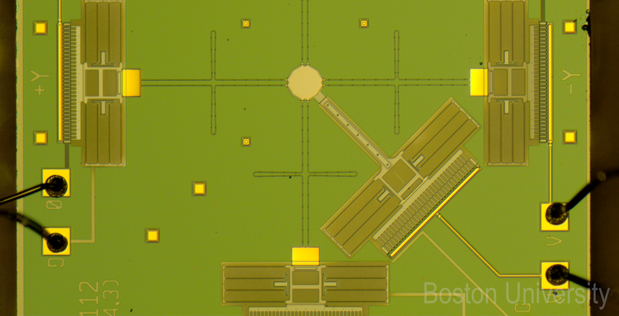
Image of a memristor chip Similarly, Lu’s electronic system is designed to detect the patterns very efficiently—and to use as few features as possible to describe the original input.
In our brains, different neurons recognize different patterns, Lu says.
“When we see an image, the neurons that recognize it will become more active,” he said. “The neurons will also compete with each other to naturally create an efficient representation. We’re implementing this approach in our electronic system.”
The researchers trained their system to learn a “dictionary” of images. Trained on a set of grayscale image patterns, their memristor network was able to reconstruct images of famous paintings and photos and other test patterns.
If their system can be scaled up, they expect to be able to process and analyze video in real time in a compact system that can be directly integrated with sensors or cameras.
The project is titled “Sparse Adaptive Local Learning for Sensing and Analytics.” Other collaborators are Zhengya Zhang and Michael Flynn of the U-M Department of Electrical Engineering and Computer Science, Garrett Kenyon of the Los Alamos National Lab and Christof Teuscher of Portland State University.
The work is part of a $6.9 million Unconventional Processing of Signals for Intelligent Data Exploitation project that aims to build a computer chip based on self-organizing, adaptive neural networks. It is funded by the [US] Defense Advanced Research Projects Agency [DARPA].
Here’s a link to and a citation for the paper,
Sparse coding with memristor networks by Patrick M. Sheridan, Fuxi Cai, Chao Du, Wen Ma, Zhengya Zhang, & Wei D. Lu. Nature Nanotechnology (2017) doi:10.1038/nnano.2017.83 Published online 22 May 2017
This paper is behind a paywall.
For the interested, there are a number of postings featuring memristors here (just use ‘memristor’ as your search term in the blog search engine). You might also want to check out ‘neuromorphic engineeering’ and ‘neuromorphic computing’ and ‘artificial brain’.
It’s usually organ-on-a-chip or lab-on-a-chip or human-on-a-chip; this is my first tree-on-a-chip.
Engineers have designed a microfluidic device they call a “tree-on-a-chip,” which mimics the pumping mechanism of trees and other plants. Courtesy: MIT
Trees and other plants, from towering redwoods to diminutive daisies, are nature’s hydraulic pumps. They are constantly pulling water up from their roots to the topmost leaves, and pumping sugars produced by their leaves back down to the roots. This constant stream of nutrients is shuttled through a system of tissues called xylem and phloem, which are packed together in woody, parallel conduits.
Now engineers at MIT [Massachusetts Institute of Technology] and their collaborators have designed a microfluidic device they call a “tree-on-a-chip,” which mimics the pumping mechanism of trees and plants. Like its natural counterparts, the chip operates passively, requiring no moving parts or external pumps. It is able to pump water and sugars through the chip at a steady flow rate for several days. The results are published this week in Nature Plants.
Anette “Peko” Hosoi, professor and associate department head for operations in MIT’s Department of Mechanical Engineering, says the chip’s passive pumping may be leveraged as a simple hydraulic actuator for small robots. Engineers have found it difficult and expensive to make tiny, movable parts and pumps to power complex movements in small robots. The team’s new pumping mechanism may enable robots whose motions are propelled by inexpensive, sugar-powered pumps.
“The goal of this work is cheap complexity, like one sees in nature,” Hosoi says. “It’s easy to add another leaf or xylem channel in a tree. In small robotics, everything is hard, from manufacturing, to integration, to actuation. If we could make the building blocks that enable cheap complexity, that would be super exciting. I think these [microfluidic pumps] are a step in that direction.”
Hosoi’s co-authors on the paper are lead author Jean Comtet, a former graduate student in MIT’s Department of Mechanical Engineering; Kaare Jensen of the Technical University of Denmark; and Robert Turgeon and Abraham Stroock, both of Cornell University.
A hydraulic lift
The group’s tree-inspired work grew out of a project on hydraulic robots powered by pumping fluids. Hosoi was interested in designing hydraulic robots at the small scale, that could perform actions similar to much bigger robots like Boston Dynamic’s Big Dog, a four-legged, Saint Bernard-sized robot that runs and jumps over rough terrain, powered by hydraulic actuators.
“For small systems, it’s often expensive to manufacture tiny moving pieces,” Hosoi says. “So we thought, ‘What if we could make a small-scale hydraulic system that could generate large pressures, with no moving parts?’ And then we asked, ‘Does anything do this in nature?’ It turns out that trees do.”
The general understanding among biologists has been that water, propelled by surface tension, travels up a tree’s channels of xylem, then diffuses through a semipermeable membrane and down into channels of phloem that contain sugar and other nutrients.
The more sugar there is in the phloem, the more water flows from xylem to phloem to balance out the sugar-to-water gradient, in a passive process known as osmosis. The resulting water flow flushes nutrients down to the roots. Trees and plants are thought to maintain this pumping process as more water is drawn up from their roots.
“This simple model of xylem and phloem has been well-known for decades,” Hosoi says. “From a qualitative point of view, this makes sense. But when you actually run the numbers, you realize this simple model does not allow for steady flow.”
In fact, engineers have previously attempted to design tree-inspired microfluidic pumps, fabricating parts that mimic xylem and phloem. But they found that these designs quickly stopped pumping within minutes.
It was Hosoi’s student Comtet who identified a third essential part to a tree’s pumping system: its leaves, which produce sugars through photosynthesis. Comtet’s model includes this additional source of sugars that diffuse from the leaves into a plant’s phloem, increasing the sugar-to-water gradient, which in turn maintains a constant osmotic pressure, circulating water and nutrients continuously throughout a tree.
Running on sugar
With Comtet’s hypothesis in mind, Hosoi and her team designed their tree-on-a-chip, a microfluidic pump that mimics a tree’s xylem, phloem, and most importantly, its sugar-producing leaves.
To make the chip, the researchers sandwiched together two plastic slides, through which they drilled small channels to represent xylem and phloem. They filled the xylem channel with water, and the phloem channel with water and sugar, then separated the two slides with a semipermeable material to mimic the membrane between xylem and phloem. They placed another membrane over the slide containing the phloem channel, and set a sugar cube on top to represent the additional source of sugar diffusing from a tree’s leaves into the phloem. They hooked the chip up to a tube, which fed water from a tank into the chip.
With this simple setup, the chip was able to passively pump water from the tank through the chip and out into a beaker, at a constant flow rate for several days, as opposed to previous designs that only pumped for several minutes.
“As soon as we put this sugar source in, we had it running for days at a steady state,” Hosoi says. “That’s exactly what we need. We want a device we can actually put in a robot.”
Hosoi envisions that the tree-on-a-chip pump may be built into a small robot to produce hydraulically powered motions, without requiring active pumps or parts.
“If you design your robot in a smart way, you could absolutely stick a sugar cube on it and let it go,” Hosoi says.
This research was supported, in part, by the Defense Advance Research Projects Agency [DARPA].
I received a March 17, 2017 Woodrow Wilson International Center for Scholars notice (via email) about this upcoming event,
The Imagineers of War: The Untold Story of DARPA [Defense Advanced Research Projects Agency], the Pentagon Agency That Changed the World
There will be a webcast of this event
In TheImagineers of War, Weinberger gives us a definitive history of the agency that has quietly shaped war and technology for nearly 60 years. Founded in 1958 in response to the launch of Sputnik, DARPA’s original mission was to create “the unimagined weapons of the future.” Over the decades, DARPA has been responsible for countless inventions and technologies that extend well beyond military technology.
Weinberger has interviewed more than one hundred former Pentagon officials and scientists involved in DARPA’s projects—many of whom have never spoken publicly about their work with the agency—and pored over countless declassified records from archives around the country, documents obtained under the Freedom of Information Act, and exclusive materials provided by sources. The Imagineers of War is a compelling and groundbreaking history in which science, technology, and politics collide.
I first heard about DARPA in reference to the internet. A developer I was working with noted that ARPA (DARPA’s predecessor agency) was instrumental in the development of the internet.
As a point of interest, the Wilson Center (also known as the Woodrow Wilson International Center for Scholars) is one of the independent agencies slated to be defunded in the 2017 US budget as proposed by President Donald Trump according to a March 16, 2017 article by Elaine Godfrey for The Atlantic.
This is exciting provided they can scale up the metamaterial for industrial use. A Feb. 9, 2017 news item on Nanowerk announces a new metamaterial that could change air conditioning from the University of Colorado at Boulder (Note: A link has been removed),
A team of University of Colorado Boulder engineers has developed a scalable manufactured metamaterial — an engineered material with extraordinary properties not found in nature — to act as a kind of air conditioning system for structures. It has the ability to cool objects even under direct sunlight with zero energy and water consumption.
When applied to a surface, the metamaterial film cools the object underneath by efficiently reflecting incoming solar energy back into space while simultaneously allowing the surface to shed its own heat in the form of infrared thermal radiation.
The new material, which is described today in the journal Science (“Scalable-manufactured randomized glass-polymer hybrid metamaterial for daytime radiative cooling”), could provide an eco-friendly means of supplementary cooling for thermoelectric power plants, which currently require large amounts of water and electricity to maintain the operating temperatures of their machinery.
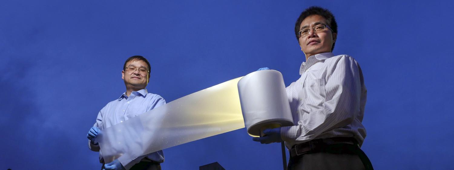
The researchers’ glass-polymer hybrid material measures just 50 micrometers thick — slightly thicker than the aluminum foil found in a kitchen — and can be manufactured economically on rolls, making it a potentially viable large-scale technology for both residential and commercial applications.
“We feel that this low-cost manufacturing process will be transformative for real-world applications of this radiative cooling technology,” said Xiaobo Yin, co-director of the research and an assistant professor who holds dual appointments in CU Boulder’s Department of Mechanical Engineering and the Materials Science and Engineering Program. Yin received DARPA’s [US Defense Advanced Research Projects Agency] Young Faculty Award in 2015.
The material takes advantage of passive radiative cooling, the process by which objects naturally shed heat in the form of infrared radiation, without consuming energy. Thermal radiation provides some natural nighttime cooling and is used for residential cooling in some areas, but daytime cooling has historically been more of a challenge. For a structure exposed to sunlight, even a small amount of directly-absorbed solar energy is enough to negate passive radiation.
The challenge for the CU Boulder researchers, then, was to create a material that could provide a one-two punch: reflect any incoming solar rays back into the atmosphere while still providing a means of escape for infrared radiation. To solve this, the researchers embedded visibly-scattering but infrared-radiant glass microspheres into a polymer film. They then added a thin silver coating underneath in order to achieve maximum spectral reflectance.
“Both the glass-polymer metamaterial formation and the silver coating are manufactured at scale on roll-to-roll processes,” added Ronggui Yang, also a professor of mechanical engineering and a Fellow of the American Society of Mechanical Engineers.
“Just 10 to 20 square meters of this material on the rooftop could nicely cool down a single-family house in summer,” said Gang Tan, an associate professor in the University of Wyoming’s Department of Civil and Architectural Engineering and a co-author of the paper.
In addition to being useful for cooling of buildings and power plants, the material could also help improve the efficiency and lifetime of solar panels. In direct sunlight, panels can overheat to temperatures that hamper their ability to convert solar rays into electricity.
“Just by applying this material to the surface of a solar panel, we can cool the panel and recover an additional one to two percent of solar efficiency,” said Yin. “That makes a big difference at scale.”
The engineers have applied for a patent for the technology and are working with CU Boulder’s Technology Transfer Office to explore potential commercial applications. They plan to create a 200-square-meter “cooling farm” prototype in Boulder in 2017.
The invention is the result of a $3 million grant awarded in 2015 to Yang, Yin and Tang by the Energy Department’s Advanced Research Projects Agency-Energy (ARPA-E).
“The key advantage of this technology is that it works 24/7 with no electricity or water usage,” said Yang “We’re excited about the opportunity to explore potential uses in the power industry, aerospace, agriculture and more.”
Members of the research team show off the metamaterial (?) Courtesy: University of Colorado at Boulder
I added the caption to this image, which was on the University of Colorado at Boulder’s home page where it accompanied the news release headline on the rotating banner.
A Sept. 23, 2016 news item on phys.org describes a way of making graphene-based medical implants safer,
In the future, our health may be monitored and maintained by tiny sensors and drug dispensers, deployed within the body and made from graphene—one of the strongest, lightest materials in the world. Graphene is composed of a single sheet of carbon atoms, linked together like razor-thin chicken wire, and its properties may be tuned in countless ways, making it a versatile material for tiny, next-generation implants.
But graphene is incredibly stiff, whereas biological tissue is soft. Because of this, any power applied to operate a graphene implant could precipitously heat up and fry surrounding cells.
Now, engineers from MIT [Massachusetts Institute of Technology] and Tsinghua University in Beijing have precisely simulated how electrical power may generate heat between a single layer of graphene and a simple cell membrane. While direct contact between the two layers inevitably overheats and kills the cell, the researchers found they could prevent this effect with a very thin, in-between layer of water.
By tuning the thickness of this intermediate water layer, the researchers could carefully control the amount of heat transferred between graphene and biological tissue. They also identified the critical power to apply to the graphene layer, without frying the cell membrane. …
Co-author Zhao Qin, a research scientist in MIT’s Department of Civil and Environmental Engineering (CEE), says the team’s simulations may help guide the development of graphene implants and their optimal power requirements.
“We’ve provided a lot of insight, like what’s the critical power we can accept that will not fry the cell,” Qin says. “But sometimes we might want to intentionally increase the temperature, because for some biomedical applications, we want to kill cells like cancer cells. This work can also be used as guidance [for those efforts.]”
…
Sandwich model
Typically, heat travels between two materials via vibrations in each material’s atoms. These atoms are always vibrating, at frequencies that depend on the properties of their materials. As a surface heats up, its atoms vibrate even more, causing collisions with other atoms and transferring heat in the process.
The researchers sought to accurately characterize the way heat travels, at the level of individual atoms, between graphene and biological tissue. To do this, they considered the simplest interface, comprising a small, 500-nanometer-square sheet of graphene and a simple cell membrane, separated by a thin layer of water.
“In the body, water is everywhere, and the outer surface of membranes will always like to interact with water, so you cannot totally remove it,” Qin says. “So we came up with a sandwich model for graphene, water, and membrane, that is a crystal clear system for seeing the thermal conductance between these two materials.”
Qin’s colleagues at Tsinghua University had previously developed a model to precisely simulate the interactions between atoms in graphene and water, using density functional theory — a computational modeling technique that considers the structure of an atom’s electrons in determining how that atom will interact with other atoms.
However, to apply this modeling technique to the group’s sandwich model, which comprised about half a million atoms, would have required an incredible amount of computational power. Instead, Qin and his colleagues used classical molecular dynamics — a mathematical technique based on a “force field” potential function, or a simplified version of the interactions between atoms — that enabled them to efficiently calculate interactions within larger atomic systems.
The researchers then built an atom-level sandwich model of graphene, water, and a cell membrane, based on the group’s simplified force field. They carried out molecular dynamics simulations in which they changed the amount of power applied to the graphene, as well as the thickness of the intermediate water layer, and observed the amount of heat that carried over from the graphene to the cell membrane.
Watery crystals
Because the stiffness of graphene and biological tissue is so different, Qin and his colleagues expected that heat would conduct rather poorly between the two materials, building up steeply in the graphene before flooding and overheating the cell membrane. However, the intermediate water layer helped dissipate this heat, easing its conduction and preventing a temperature spike in the cell membrane.
Looking more closely at the interactions within this interface, the researchers made a surprising discovery: Within the sandwich model, the water, pressed against graphene’s chicken-wire pattern, morphed into a similar crystal-like structure.
“Graphene’s lattice acts like a template to guide the water to form network structures,” Qin explains. “The water acts more like a solid material and makes the stiffness transition from graphene and membrane less abrupt. We think this helps heat to conduct from graphene to the membrane side.”
The group varied the thickness of the intermediate water layer in simulations, and found that a 1-nanometer-wide layer of water helped to dissipate heat very effectively. In terms of the power applied to the system, they calculated that about a megawatt of power per meter squared, applied in tiny, microsecond bursts, was the most power that could be applied to the interface without overheating the cell membrane.
Qin says going forward, implant designers can use the group’s model and simulations to determine the critical power requirements for graphene devices of different dimensions. As for how they might practically control the thickness of the intermediate water layer, he says graphene’s surface may be modified to attract a particular number of water molecules.
“I think graphene provides a very promising candidate for implantable devices,” Qin says. “Our calculations can provide knowledge for designing these devices in the future, for specific applications, like sensors, monitors, and other biomedical applications.”
This research was supported in part by the MIT International Science and Technology Initiative (MISTI): MIT-China Seed Fund, the National Natural Science Foundation of China, DARPA [US Defense Advanced Research Projects Agency], the Department of Defense (DoD) Office of Naval Research, the DoD Multidisciplinary Research Initiatives program, the MIT Energy Initiative, and the National Science Foundation.
… the path to greater benefits – whether economic, social, or environmental – from nanomanufactured goods and services is not yet clear. A recent review article in ACS Nano (“Nanomanufacturing: A Perspective”) by J. Alexander Liddle and Gregg M. Gallatin, takes silicon integrated circuit manufacturing as a baseline in order to consider the factors involved in matching processes with products, examining the characteristics and potential of top-down and bottom-up processes, and their combination.
The authors also discuss how a careful assessment of the way in which function can be made to follow form can enable high-volume manufacturing of nanoscale structures with the desired useful, and exciting, properties.
Although often used interchangeably, it makes sense to distinguish between nanofabrication and nanomanufacturing using the criterion of economic viability, suggested by the connotations of industrial scale and profitability associated with the word ‘manufacturing’.
Here’s a link to and a citation for the paper Berger is reviewing,
Nanomanufacturing: A Perspective by J. Alexander Liddle and Gregg M. Gallatin. ACS Nano, 2016, 10 (3), pp 2995–3014 DOI: 10.1021/acsnano.5b03299 Publication Date (Web): February 10, 2016
Copyright This article not subject to U.S. Copyright. Published 2016 by the American Chemical Society
This paper is behind a paywall.
Luckily for those who’d like a little more information before purchase, Berger’s review provides some insight into the study additional to what you’ll find in the abstract,
Nanomanufacturing, as the authors define it in their article, therefore, has the salient characteristic of being a source of money, while nanofabrication is often a sink.
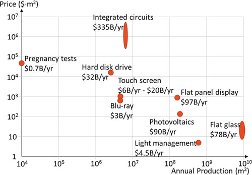
To supply some background and indicate the scale of the nanomanufacturing challenge, the figure below shows the selling price ($·m-2) versus the annual production (m2) for a variety of nanoenabled or potentially nanoenabled products. The overall global market sizes are also indicated. It is interesting to note that the selling price spans 5 orders of magnitude, the production six, and the market size three. Although there is no strong correlation between the variables,
market price and size nanoenabled product
Log-log plot of the approximate product selling price ($·m-2) versus global annual production (m2) for a variety of nanoenabled, or potentially nanoenabled products. Approximate market sizes (2014) are shown next to each point. (Reprinted with permission by American Chemical Society)
Log-log plot of the approximate product selling price ($·m-2) versus global annual production (m2) for a variety of nanoenabled, or potentially nanoenabled products. Approximate market sizes (2014) are shown next to each point. (Reprinted with permission by American Chemical Society)
I encourage anyone interested in nanomanufacturing to read Berger’s article in its entirety as there is more detail and there are more figures to illustrate the points being made. He ends his review with this,
“Perhaps the most exciting prospect is that of creating dynamical nanoscale systems that are capable of exhibiting much richer structures and functionality. Whether this is achieved by learning how to control and engineer biological systems directly, or by building systems based on the same principles, remains to be seen, but will undoubtedly be disruptive and quite probably revolutionary.”
I find the reference to biological systems quite interesting especially in light of the recent launch of DARPA’s (US Defense Advanced Research Projects Agency) Engineered Living Materials (ELM) program (see my Aug. 9, 2016 posting).
DARPA (US Defense Advanced Research Projects Agency) has launched a program called Engineered Living Materials (ELM) and issued an invitation. From an Aug. 9, 2016 news item on Nanowerk,
The structural materials that are currently used to construct homes, buildings, and infrastructure are expensive to produce and transport, wear out due to age and damage, and have limited ability to respond to changes in their immediate surroundings. Living biological materials—bone, skin, bark, and coral, for example—have attributes that provide advantages over the non-living materials people build with, in that they can be grown where needed, self-repair when damaged, and respond to changes in their surroundings. The inclusion of living materials in human-built environments could offer significant benefits; however, today scientists and engineers are unable to easily control the size and shape of living materials in ways that would make them useful for construction.
DARPA is launching the Engineered Living Materials (ELM) program with a goal of creating a new class of materials that combines the structural properties of traditional building materials with attributes of living systems. Living materials represent a new opportunity to leverage engineered biology to solve existing problems associated with the construction and maintenance of built environments, and to create new capabilities to craft smart infrastructure that dynamically responds to its surroundings.
“The vision of the ELM program is to grow materials on demand where they are needed,” said ELM program manager Justin Gallivan. “Imagine that instead of shipping finished materials, we can ship precursors and rapidly grow them on site using local resources. And, since the materials will be alive, they will be able to respond to changes in their environment and heal themselves in response to damage.”
Grown materials are not entirely new, but their current manifestations differ substantially from the materials Gallivan envisions. For instance, biologically sourced structural materials can already be grown into specified sizes and shapes from inexpensive feedstocks; packing materials derived from fungal mycelium and building blocks made from bacteria and sand are two modern examples. And, of course, wood has been used for ages. However, these products are rendered inert during the manufacturing process, so they exhibit few of their components’ original biological advantages. Scientists are making progress with three-dimensional printing of living tissues and organs, using scaffolding materials that sustain the long-term viability of the living cells. These cells are derived from existing natural tissues, however, and are not engineered to perform synthetic functions. And current cell-printing methods are too expensive to produce building materials at necessary scales.
ELM looks to merge the best features of these existing technologies and build on them to create hybrid materials composed of non-living scaffolds that give structure to and support the long-term viability of engineered living cells. DARPA intends to develop platform technologies that are scalable and generalizable to facilitate a quick transition from laboratory to commercial applications.
The long-term objective of the ELM program is to develop an ability to engineer structural properties directly into the genomes of biological systems so that neither scaffolds nor external development cues are needed for an organism to realize the desired shape and properties. Achieving this goal will require significant breakthroughs in scientists’ understanding of developmental pathways and how those pathways direct the three-dimensional development of multicellular systems.
Work on ELM will be fundamental research carried out in controlled laboratory settings. DARPA does not anticipate environmental release during the program.
For anyone who’s interested in participating in the program, there’s an announcement (download the PDF for more details) featuring a Proposers Day event on Aug. 26, 2016 being held in Arlington, Virginia,
The Proposers Day objectives are:
1) To introduce the science and technology community (industry, academia, and government) to the ELM program vision and goals;
2) To facilitate interaction between investigators that may have capabilities to develop elements of interest and relevance to ELM goals; and
3) To encourage and promote teaming arrangements among organizations that have the relevant expertise, research facilities and capabilities for executing research and development responsive to the ELM program goals.
The Proposers Day will include overview presentations and optional sidebar meetings where potential proposers can discuss ideas for proposal submissions with the Government team.
The goal of the DARPA ELM program is to explore and develop living materials that combine the structural properties of traditional building materials with attributes of living systems, including the ability to rapidly grow, to self-repair, and to adapt to the environment. Living materials represent a new opportunity to leverage engineered biology to solve existing problems associated with the construction and maintenance of our built environments, as well as to create new capabilities to craft smart infrastructure that dynamically responds to our surroundings. The specific program objectives are to develop design tools and methods that enable the engineering of structural features into cellular systems that function as living materials, thereby opening up a new design space for building technology. These new methods will be validated by the production of living materials that can reproduce, self-organize and self-heal.
This research from Singapore could make neuroprosthetics and exoskeletons a little easier to manage as long as you don’t mind having a neural implant. From a Feb. 11, 2016 news item on ScienceDaily,
A versatile chip offers multiple applications in various electronic devices, report researchers, suggested that there is now hope that a low-powered, wireless neural implant may soon be a reality. Neural implants when embedded in the brain can alleviate the debilitating symptoms of Parkinson’s disease or give paraplegic people the ability to move their prosthetic limbs.
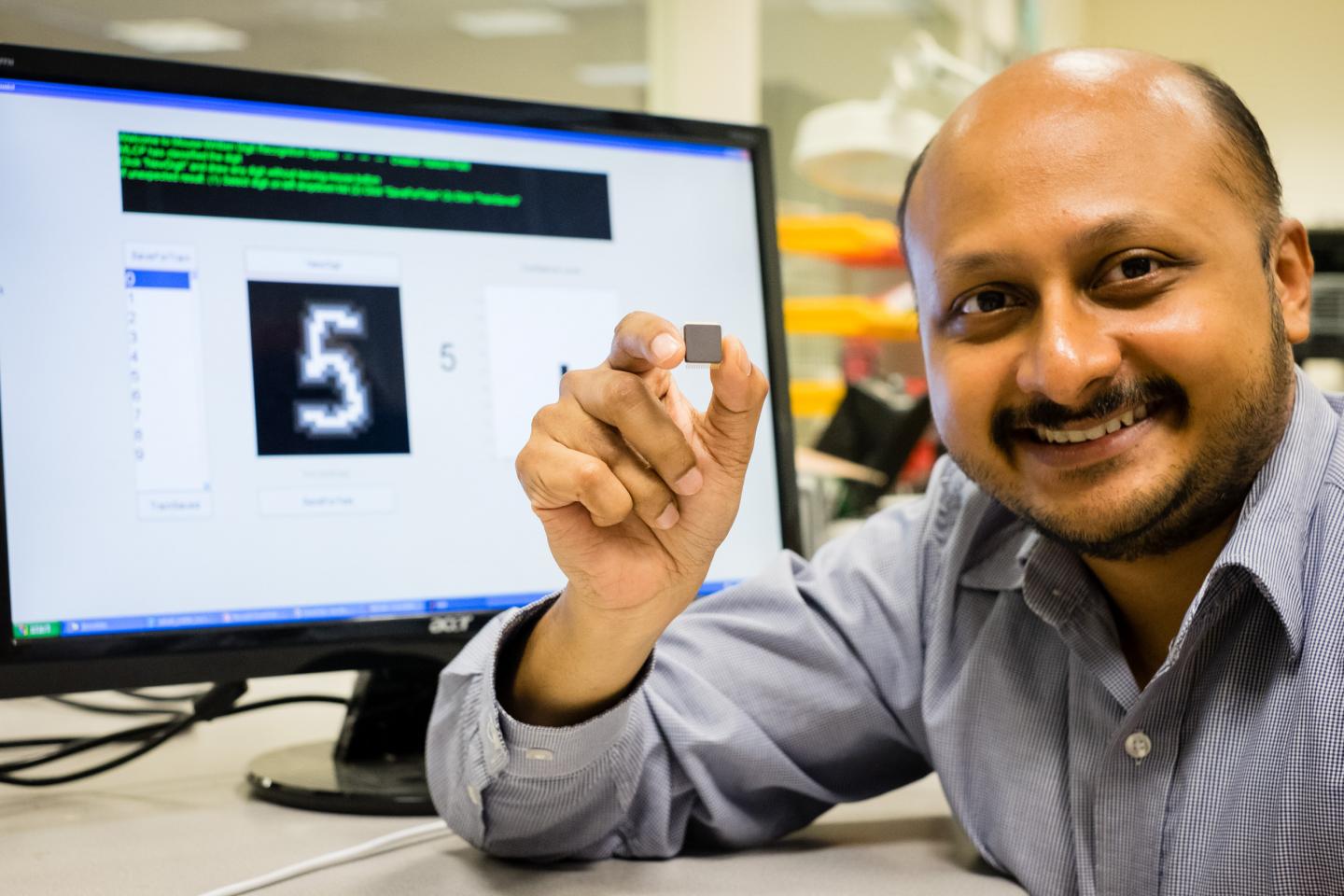
Caption: NTU Asst Prof Arindam Basu is holding his low-powered smart chip. Credit: NTU Singapore
Scientists at Nanyang Technological University, Singapore (NTU Singapore) have developed a small smart chip that can be paired with neural implants for efficient wireless transmission of brain signals.
Neural implants when embedded in the brain can alleviate the debilitating symptoms of Parkinson’s disease or give paraplegic people the ability to move their prosthetic limbs.
However, they need to be connected by wires to an external device outside the body. For a prosthetic patient, the neural implant is connected to a computer that decodes the brain signals so the artificial limb can move.
These external wires are not only cumbersome but the permanent openings which allow the wires into the brain increases the risk of infections.
The new chip by NTU scientists can allow the transmission of brain data wirelessly and with high accuracy.
Assistant Professor Arindam Basu from NTU’s School of Electrical and Electronic Engineering said the research team have tested the chip on data recorded from animal models, which showed that it could decode the brain’s signal to the hand and fingers with 95 per cent accuracy.
“What we have developed is a very versatile smart chip that can process data, analyse patterns and spot the difference,” explained Prof Basu.
“It is about a hundred times more efficient than current processing chips on the market. It will lead to more compact medical wearable devices, such as portable ECG monitoring devices and neural implants, since we no longer need large batteries to power them.”
Different from other wireless implants
To achieve high accuracy in decoding brain signals, implants require thousands of channels of raw data. To wirelessly transmit this large amount of data, more power is also needed which means either bigger batteries or more frequent recharging.
This is not feasible as there is limited space in the brain for implants while frequent recharging means the implants cannot be used for long-term recording of signals.
Current wireless implant prototypes thus suffer from a lack of accuracy as they lack the bandwidth to send out thousands of channels of raw data.
Instead of enlarging the power source to support the transmission of raw data, Asst Prof Basu tried to reduce the amount of data that needs to be transmitted.
Designed to be extremely power-efficient, NTU’s patented smart chip will analyse and decode the thousands of signals from the neural implants in the brain, before compressing the results and sending it wirelessly to a small external receiver.
This invention and its findings were published last month [December 2015] in the prestigious journal, IEEE Transactions on Biomedical Circuits & Systems, by the Institute of Electrical and Electronics Engineers, the world’s largest professional association for the advancement of technology.
Its underlying science was also featured in three international engineering conferences (two in Atlanta, USA and one in China) over the last three months.
Versatile smart chip with multiple uses
This new smart chip is designed to analyse data patterns and spot any abnormal or unusual patterns.
For example, in a remote video camera, the chip can be programmed to send a video back to the servers only when a specific type of car or something out of the ordinary is detected, such as an intruder.
This would be extremely beneficial for the Internet of Things (IOT), where every electrical and electronic device is connected to the Internet through a smart chip.
With a report by marketing research firm Gartner Inc predicting that 6.4 billion smart devices and appliances will be connected to the Internet by 2016, and will rise to 20.8 billion devices by 2020, reducing network traffic will be a priority for most companies.
Using NTU’s new chip, the devices can process and analyse the data on site, before sending back important details in a compressed package, instead of sending the whole data stream. This will reduce data usage by over a thousand times.
Asst Prof Basu is now in talks with Singapore Technologies Electronics Limited to adapt his smart chip that can significantly reduce power consumption and the amount of data transmitted by battery-operated remote sensors, such as video cameras.
The team is also looking to expand the applications of the chip into commercial products, such as to customise it for smart home sensor networks, in collaboration with a local electronics company.
The chip, measuring 5mm by 5mm can now be licensed by companies from NTU’s commercialisation arm, NTUitive.
Earlier this month there was a Feb. 9, 2016 announcement about a planned human clinical trial in Australia for a new brain-machine interface (neural implant). Before proceeding with the news, here’s what this implant looks like,
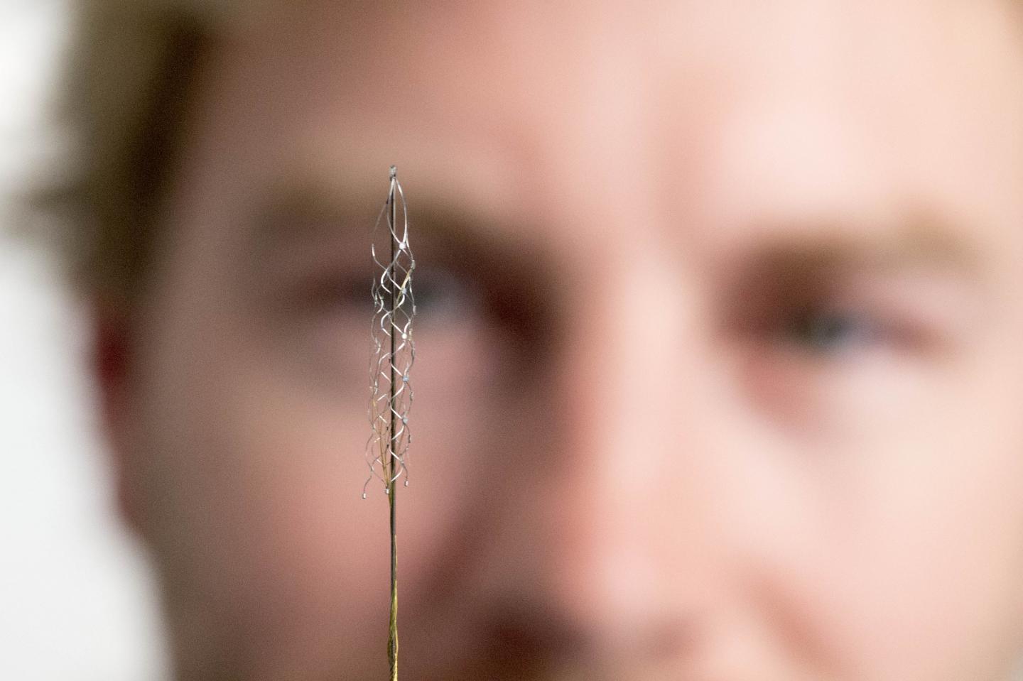
Caption: This tiny device, the size of a small paperclip, is implanted in to a blood vessel next to the brain and can read electrical signals from the motor cortex, the brain’s control centre. These signals can then be transmitted to an exoskeleton or wheelchair to give paraplegic patients greater mobility. Users will need to learn how to communicate with their machinery, but over time, it is thought it will become second nature, like driving or playing the piano. The first human trials are slated for 2017 in Melbourne, Australia. Credit: The University of Melbourne.
Melbourne medical researchers have created a new minimally invasive brain-machine interface, giving people with spinal cord injuries new hope to walk again with the power of thought.
The brain machine interface consists of a stent-based electrode (stentrode), which is implanted within a blood vessel next to the brain, and records the type of neural activity that has been shown in pre-clinical trials to move limbs through an exoskeleton or to control bionic limbs.
The new device is the size of a small paperclip and will be implanted in the first in-human trial at The Royal Melbourne Hospital in 2017.
The results published today in Nature Biotechnology show the device is capable of recording high-quality signals emitted from the brain’s motor cortex, without the need for open brain surgery.
Principal author and Neurologist at The Royal Melbourne Hospital and Research Fellow at The Florey Institute of Neurosciences and the University of Melbourne, Dr Thomas Oxley, said the stentrode was revolutionary.
“The development of the stentrode has brought together leaders in medical research from The Royal Melbourne Hospital, The University of Melbourne and the Florey Institute of Neuroscience and Mental Health. In total 39 academic scientists from 16 departments were involved in its development,” Dr Oxley said.
“We have been able to create the world’s only minimally invasive device that is implanted into a blood vessel in the brain via a simple day procedure, avoiding the need for high risk open brain surgery.
“Our vision, through this device, is to return function and mobility to patients with complete paralysis by recording brain activity and converting the acquired signals into electrical commands, which in turn would lead to movement of the limbs through a mobility assist device like an exoskeleton. In essence this a bionic spinal cord.”
Stroke and spinal cord injuries are leading causes of disability, affecting 1 in 50 people. There are 20,000 Australians with spinal cord injuries, with the typical patient a 19-year old male, and about 150,000 Australians left severely disabled after stroke.
Co-principal investigator and biomedical engineer at the University of Melbourne, Dr Nicholas Opie, said the concept was similar to an implantable cardiac pacemaker – electrical interaction with tissue using sensors inserted into a vein, but inside the brain.
“Utilising stent technology, our electrode array self-expands to stick to the inside wall of a vein, enabling us to record local brain activity. By extracting the recorded neural signals, we can use these as commands to control wheelchairs, exoskeletons, prosthetic limbs or computers,” Dr Opie said.
“In our first-in-human trial, that we anticipate will begin within two years, we are hoping to achieve direct brain control of an exoskeleton for three people with paralysis.”
“Currently, exoskeletons are controlled by manual manipulation of a joystick to switch between the various elements of walking – stand, start, stop, turn. The stentrode will be the first device that enables direct thought control of these devices”
Neurophysiologist at The Florey, Professor Clive May, said the data from the pre-clinical study highlighted that the implantation of the device was safe for long-term use.
“Through our pre-clinical study we were able to successfully record brain activity over many months. The quality of recording improved as the device was incorporated into tissue,” Professor May said.
“Our study also showed that it was safe and effective to implant the device via angiography, which is minimally invasive compared with the high risks associated with open brain surgery.
“The brain-computer interface is a revolutionary device that holds the potential to overcome paralysis, by returning mobility and independence to patients affected by various conditions.”
Professor Terry O’Brien, Head of Medicine at Departments of Medicine and Neurology, The Royal Melbourne Hospital and University of Melbourne said the development of the stentrode has been the “holy grail” for research in bionics.
“To be able to create a device that can record brainwave activity over long periods of time, without damaging the brain is an amazing development in modern medicine,” Professor O’Brien said.
“It can also be potentially used in people with a range of diseases aside from spinal cord injury, including epilepsy, Parkinsons and other neurological disorders.”
The development of the minimally invasive stentrode and the subsequent pre-clinical trials to prove its effectiveness could not have been possible without the support from the major funding partners – US Defense Department DARPA [Defense Advanced Research Projects Agency] and Australia’s National Health and Medical Research Council.
So, DARPA is helping fund this, eh? Interesting but not a surprise given the agency’s previous investments in brain research and neuroprosthetics.
For those who like to get their news via video,
Here’s a link to and a citation for the paper,
Minimally invasive endovascular stent-electrode array for high-fidelity, chronic recordings of cortical neural activity by Thomas J Oxley, Nicholas L Opie, Sam E John, Gil S Rind, Stephen M Ronayne, Tracey L Wheeler, Jack W Judy, Alan J McDonald, Anthony Dornom, Timothy J H Lovell, Christopher Steward, David J Garrett, Bradford A Moffat, Elaine H Lui, Nawaf Yassi, Bruce C V Campbell, Yan T Wong, Kate E Fox, Ewan S Nurse, Iwan E Bennett, Sébastien H Bauquier, Kishan A Liyanage, Nicole R van der Nagel, Piero Perucca, Arman Ahnood et al. Nature Biotechnology (2016) doi:10.1038/nbt.3428 Published online 08 February 2016
This paper is behind a paywall.
I wish the researchers in Singapore, Australia, and elsewhere, good luck!
*’Sinagpore’ in head changed to ‘Singapore’ on May 14, 2019.
Gregory Carpenter has written a gripping (albeit somewhat exaggerated) piece for Signal, a publication of the Armed Forces Communications and Electronics Association (AFCEA) about cybersecurity issues and nanomedicine endeavours. From Carpenter’s Jan. 1, 2016 article titled, When Lifesaving Technology Can Kill; The Cyber Edge,
The exciting advent of nanotechnology that has inspired disruptive and lifesaving medical advances is plagued by cybersecurity issues that could result in the deaths of people that these very same breakthroughs seek to heal. Unfortunately, nanorobotic technology has suffered from the same security oversights that afflict most other research and development programs.
Nanorobots, or small machines [or nanobots[, are vulnerable to exploitation just like other devices.
At the moment, the issue of cybersecurity exploitation is secondary to making nanobots, or nanorobots, dependably functional. As far as I’m aware, there is no such nanobot. Even nanoparticles meant to function as packages for drug delivery have not been perfected (see one of the controversies with nanomedicine drug delivery described in my Nov. 26, 2015 posting).
That said, Carpenter’s point about cybersecurity is well taken since security features are often overlooked in new technology. For example, automated banking machines (ABMs) had woefully poor (inadequate, almost nonexistent) security when they were first introduced.
Carpenter outlines some of the problems that could occur, assuming some of the latest research could be reliably brought to market,
The U.S. military has joined the fray of nanorobotic experimentation, embarking on revolutionary research that could lead to a range of discoveries, from unraveling the secrets of how brains function to figuring out how to permanently purge bad memories. Academia is making amazing advances as well. Harnessing progress by Harvard scientists to move nanorobots within humans, researchers at the University of Montreal, Polytechnique Montreal and Centre Hospitalier Universitaire Sainte-Justine are using mobile nanoparticles inside the human brain to open the blood-brain barrier, which protects the brain from toxins found in the circulatory system.
…
A different type of technology presents a risk similar to the nanoparticles scenario. A DARPA-funded program known as Restoring Active Memory (RAM) addresses post-traumatic stress disorder, attempting to overcome memory deficits by developing neuroprosthetics that bridge gaps in an injured brain. In short, scientists can wipe out a traumatic memory, and they hope to insert a new one—one the person has never actually experienced. Someone could relish the memory of a stroll along the French Riviera rather than a terrible firefight, even if he or she has never visited Europe.
As an individual receives a disruptive memory, a cyber criminal could manage to hack the controls. Breaches of the brain could become a reality, putting humans at risk of becoming zombie hosts [emphasis mine] for future virus deployments. …
At this point, the ‘zombie’ scenario Carpenter suggests seems a bit over-the-top but it does hearken to the roots of the zombie myth where the undead aren’t mindlessly searching for brains but are humans whose wills have been overcome. Mike Mariani in an Oct. 28, 2015 article for The Atlantic has presented a thought-provoking history of zombies,
… the zombie myth is far older and more rooted in history than the blinkered arc of American pop culture suggests. It first appeared in Haiti in the 17th and 18th centuries, when the country was known as Saint-Domingue and ruled by France, which hauled in African slaves to work on sugar plantations. Slavery in Saint-Domingue under the French was extremely brutal: Half of the slaves brought in from Africa were worked to death within a few years, which only led to the capture and import of more. In the hundreds of years since, the zombie myth has been widely appropriated by American pop culture in a way that whitewashes its origins—and turns the undead into a platform for escapist fantasy.
The original brains-eating fiend was a slave not to the flesh of others but to his own. The zombie archetype, as it appeared in Haiti and mirrored the inhumanity that existed there from 1625 to around 1800, was a projection of the African slaves’ relentless misery and subjugation. Haitian slaves believed that dying would release them back to lan guinée, literally Guinea, or Africa in general, a kind of afterlife where they could be free. Though suicide was common among slaves, those who took their own lives wouldn’t be allowed to return to lan guinée. Instead, they’d be condemned to skulk the Hispaniola plantations for eternity, an undead slave at once denied their own bodies and yet trapped inside them—a soulless zombie.
I recommend reading Mariani’s article although I do have one nit to pick. I can’t find a reference to brain-eating zombies until George Romero’s introduction of the concept in his movies. This Zombie Wikipedia entry seems to be in agreement with my understanding (if I’m wrong, please do let me know and, if possible, provide a link to the corrective text).
Getting back to Carpenter and cybersecurity with regard to nanomedicine, while his scenarios may seem a trifle extreme it’s precisely the kind of thinking you need when attempting to anticipate problems. I do wish he’d made clear that the technology still has a ways to go.
It took over a year after announcing the ‘Atoms to Product’ program in 2014 for DARPA (US Defense Advanced Research Projects Agency) to select 10 proponents for three projects. Before moving onto the latest announcement, here’s a description of the ‘Atoms to Product’ program from its Aug. 27, 2014 announcement on Nanowerk,
Many common materials exhibit different and potentially useful characteristics when fabricated at extremely small scales—that is, at dimensions near the size of atoms, or a few ten-billionths of a meter. These “atomic scale” or “nanoscale” properties include quantized electrical characteristics, glueless adhesion, rapid temperature changes, and tunable light absorption and scattering that, if available in human-scale products and systems, could offer potentially revolutionary defense and commercial capabilities. Two as-yet insurmountable technical challenges, however, stand in the way: Lack of knowledge of how to retain nanoscale properties in materials at larger scales, and lack of assembly capabilities for items between nanoscale and 100 microns—slightly wider than a human hair.
DARPA has created the Atoms to Product (A2P) program to help overcome these challenges. The program seeks to develop enhanced technologies for assembling atomic-scale pieces. It also seeks to integrate these components into materials and systems from nanoscale up to product scale in ways that preserve and exploit distinctive nanoscale properties.
DARPA’s Atoms to Product (A2P) program seeks to develop enhanced technologies for assembling nanoscale items, and integrating these components into materials and systems from nanoscale up to product scale in ways that preserve and exploit distinctive nanoscale properties.
DARPA recently selected 10 performers to tackle this challenge: Zyvex Labs, Richardson, Texas; SRI, Menlo Park, California; Boston University, Boston, Massachusetts; University of Notre Dame, South Bend, Indiana; HRL Laboratories, Malibu, California; PARC, Palo Alto, California; Embody, Norfolk, Virginia; Voxtel, Beaverton, Oregon; Harvard University, Cambridge, Massachusetts; and Draper Laboratory, Cambridge, Massachusetts.
A Dec. 29, 2015 DARPA news release, which originated the news item, offers more information and an image illustrating the type of advances already made by one of the successful proponents,
DARPA recently launched its Atoms to Product (A2P) program, with the goal of developing technologies and processes to assemble nanometer-scale pieces—whose dimensions are near the size of atoms—into systems, components, or materials that are at least millimeter-scale in size. At the heart of that goal was a frustrating reality: Many common materials, when fabricated at nanometer-scale, exhibit unique and attractive “atomic-scale” behaviors including quantized current-voltage behavior, dramatically lower melting points and significantly higher specific heats—but they tend to lose these potentially beneficial traits when they are manufactured at larger “product-scale” dimensions, typically on the order of a few centimeters, for integration into devices and systems.
…
“The ability to assemble atomic-scale pieces into practical components and products is the key to unlocking the full potential of micromachines,” said John Main, DARPA program manager. “The DARPA Atoms to Product Program aims to bring the benefits of microelectronic-style miniaturization to systems and products that combine mechanical, electrical, and chemical processes.”
The program calls for closing the assembly gap in two steps: From atoms to microns and from microns to millimeters. Performers are tasked with addressing one or both of these steps and have been assigned to one of three working groups, each with a distinct focus area.
…
Image caption: Microscopic tools such as this nanoscale “atom writer” can be used to fabricate minuscule light-manipulating structures on surfaces. DARPA has selected 10 performers for its Atoms to Product (A2P) program whose goal is to develop technologies and processes to assemble nanometer-scale pieces—whose dimensions are near the size of atoms—into systems, components, or materials that are at least millimeter-scale in size. (Image credit: Boston University)
Here’s more about the projects and the performers (proponents) from the A2P performers page on the DARPA website,
Nanometer to Millimeter in a Single System – Embody, Draper and Voxtel
Current methods to treat ligament injuries in warfighters [also known as, soldiers]—which account for a significant portion of reported injuries—often fail to restore pre-injury performance, due to surgical complexities and an inadequate supply of donor tissue. Embody is developing reinforced collagen nanofibers that mimic natural ligaments and replicate the biological and biomechanical properties of native tissue. Embody aims to create a new standard of care and restore pre-injury performance for warfighters and sports injury patients at a 50% reduction compared to current costs.
Radio Frequency (RF) systems (e.g., cell phones, GPS) have performance limits due to alternating current loss. In lower frequency power systems this is addressed by braiding the wires, but this is not currently possibly in cell phones due to an inability to manufacture sufficiently small braided wires. Draper is developing submicron wires that can be braided using DNA self-assembly methods. If successful, portable RF systems will be more power efficient and able to send 10 times more information in a given channel.
For seamless control of structures, physics and surface chemistry—from the atomic-level to the meter-level—Voxtel Inc. and partner Oregon State University are developing an efficient, high-rate, fluid-based manufacturing process designed to imitate nature’s ability to manufacture complex multimaterial products across scales. Historically, challenges relating to the cost of atomic-level control, production speed, and printing capability have been effectively insurmountable. This team’s new process will combine synthesis and delivery of materials into a massively parallel inkjet operation that draws from nature to achieve a DNA-like mediated assembly. The goal is to assemble complex, 3-D multimaterial mixed organic and inorganic products quickly and cost-effectively—directly from atoms.
Optical Metamaterial Assembly – Boston University, University of Notre Dame, HRL and PARC.
Nanoscale devices have demonstrated nearly unlimited power and functionality, but there hasn’t been a general- purpose, high-volume, low-cost method for building them. Boston University is developing an atomic calligraphy technique that can spray paint atoms with nanometer precision to build tunable optical metamaterials for the photonic battlefield. If successful, this capability could enhance the survivability of a wide range of military platforms, providing advanced camouflage and other optical illusions in the visual range much as stealth technology has enabled in the radar range.
The University of Notre Dame is developing massively parallel nanomanufacturing strategies to overcome the requirement today that most optical metamaterials must be fabricated in “one-off” operations. The Notre Dame project aims to design and build optical metamaterials that can be reconfigured to rapidly provide on-demand, customized optical capabilities. The aim is to use holographic traps to produce optical “tiles” that can be assembled into a myriad of functional forms and further customized by single-atom electrochemistry. Integrating these materials on surfaces and within devices could provide both warfighters and platforms with transformational survivability.
HRL Laboratories is working on a fast, scalable and material-agnostic process for improving infrared (IR) reflectivity of materials. Current IR-reflective materials have limited use, because reflectivity is highly dependent on the specific angle at which light hits the material. HRL is developing a technique for allowing tailorable infrared reflectivity across a variety of materials. If successful, the process will enable manufacturable materials with up to 98% IR reflectivity at all incident angles.
PARC is working on building the first digital MicroAssembly Printer, where the “inks” are micrometer-size particles and the “image” outputs are centimeter-scale and larger assemblies. The goal is to print smart materials with the throughput and cost of laser printers, but with the precision and functionality of nanotechnology. If successful, the printer would enable the short-run production of large, engineered, customized microstructures, such as metamaterials with unique responses for secure communications, surveillance and electronic warfare.
Flexible, General Purpose Assembly – Zyvex, SRI, and Harvard.
Zyvex aims to create nano-functional micron-scale devices using customizable and scalable manufacturing that is top-down and atomically precise. These high-performance electronic, optical, and nano-mechanical components would be assembled by SRI micro-robots into fully-functional devices and sub-systems such as ultra-sensitive sensors for threat detection, quantum communication devices, and atomic clocks the size of a grain of sand.
SRI’s Levitated Microfactories will seek to combine the precision of MEMS [micro-electromechanical systems] flexures with the versatility and range of pick-and-place robots and the scalability of swarms [an idea Michael Crichton used in his 2002 novel Prey to induce horror] to assemble and electrically connect micron and millimeter components to build stronger materials, faster electronics, and better sensors.
Many high-impact, minimally invasive surgical techniques are currently performed only by elite surgeons due to the lack of tactile feedback at such small scales relative to what is experienced during conventional surgical procedures. Harvard is developing a new manufacturing paradigm for millimeter-scale surgical tools using low-cost 2D layer-by-layer processes and assembly by folding, resulting in arbitrarily complex meso-scale 3D devices. The goal is for these novel tools to restore the necessary tactile feedback and thereby nurture a new degree of dexterity to perform otherwise demanding micro- and minimally invasive surgeries, and thus expand the availability of life-saving procedures.
Sidebar
‘Sidebar’ is my way of indicating these comments have little to do with the matter at hand but could be interesting factoids for you.
First, Zyvex Labs was last mentioned here in a Sept. 10, 2014 posting titled: OCSiAL will not be acquiring Zyvex. Notice that this announcement was made shortly after DARPA’s A2P program was announced and that OCSiAL is one of RUSNANO’s (a Russian funding agency focused on nanotechnology) portfolio companies (see my Oct. 23, 2015 posting for more).
HRL Laboratories, mentioned here in an April 19, 2012 posting mostly concerned with memristors (nanoscale devices that mimic neural or synaptic plasticity), has its roots in Howard Hughes’s research laboratories as noted in the posting. In 2012, HRL was involved in another DARPA project, SyNAPSE.
Finally and minimally, PARC also known as, Xerox PARC, was made famous by Steven Jobs and Steve Wozniak when they set up their own company (Apple) basing their products on innovations that PARC had rejected. There are other versions of the story and one by Malcolm Gladwell for the New Yorker May 16, 2011 issue which presents a more complicated and, at times, contradictory version of that particular ‘origins’ story.
Image of a memristor chip Similarly, Lu’s electronic system is designed to detect the patterns very efficiently—and to use as few features as possible to describe the original input.