Tag Archives: David Chandler

Silk micro or nanoparticles for tracking seeds

I hadn’t heard of counterfeit seeds before but this March 22, 2023 news item on phys.org describes the problem and announces an approach to prevention,

Average crop yields in Africa are consistently far below expected, and one significant reason is the prevalence of counterfeit seeds whose germination rates are far lower than those of the genuine ones. The World Bank estimates that as much as half of all seeds sold in some African countries are fake, which could help to account for crop production that is far below potential.

There have been many attempts to prevent this counterfeiting through tracking labels, but none have proved effective; among other issues, such labels have been vulnerable to hacking because of the deterministic nature of their encoding systems. But now, a team of MIT [Massachusetts Institute of Technology] researchers has come up with a kind of tiny, biodegradable tag that can be applied directly to the seeds themselves, and that provides a unique randomly created code that cannot be duplicated.

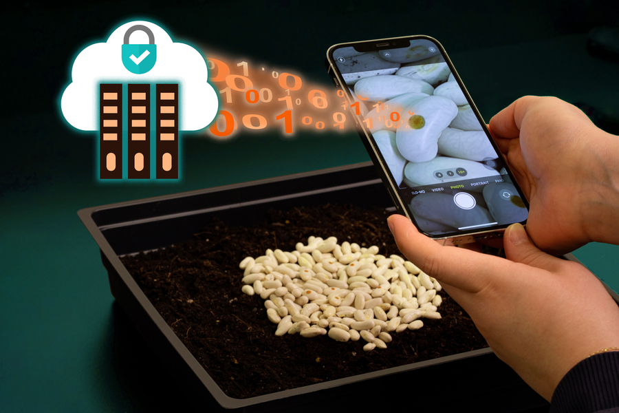
I found this picture helped me to understand how ‘tracking’ these seeds could be useful,

As a way to reduce seed counterfeiting, MIT researchers developed a silk-based tag that, when applied to seeds, provides a unique code that cannot be duplicated. Credits: Credit: Photograph courtesy of the researchers. Edited by Jose-Luis Olivares, MIT

A March 22, 2023 Massachusetts Institute of Technology (MIT) news release by David Chandler (also on EurekAlert), which originated the news item, describes the work in more detail (Note: I’m glad to see David Chandler is getting bylines again even if it’s on the EurekAlert version only),

The new system, which uses minuscule dots of silk-based material, each containing a unique combination of different chemical signatures, is described today in the journal Science Advances in a paper by MIT’s dean of engineering Anantha Chandrakasan, professor of civil and environmental engineering Benedetto Marelli, postdoc Hui Sun, and graduate student Saurav Maji.

The problem of counterfeiting is an enormous one globally, the researchers point out, affecting everything from drugs to luxury goods, and many different systems have been developed to try to combat this. But there has been less attention to the problem in the area of agriculture, even though the consequences can be severe. In sub-Saharan Africa, for example, the World Bank estimates that counterfeit seeds are a significant factor in crop yields that average less than one-fifth of the potential for maize, and less than one-third for rice. 

Marelli explains that a key to the new system is creating a randomly-produced physical object whose exact composition is virtually impossible to duplicate. The labels they create “leverage randomness and uncertainty in the process of application, to generate unique signature features that can be read, and that cannot be replicated,” he says.

What they’re dealing with, Sun adds, “is the very old job of trying, basically, not to get your stuff stolen. And you can try as much as you can, but eventually somebody is always smart enough to figure out how to do it, so nothing is really unbreakable. But the idea is, it’s almost impossible, if not impossible, to replicate it, or it takes so much effort that it’s not worth it anymore.”

The idea of an “unclonable” code was originally developed as a way of protecting the authenticity of computer chips, explains Chandrakasan, who is the Vannevar Bush Professor of Electrical Engineering and Computer Science. “In integrated circuits, individual transistors have slightly different properties coined device variations,” he explains, “and you could then use that variability and combine that variability with higher-level circuits to create a unique ID for the device. And once you have that, then you can use that unique ID as a part of a security protocol. Something like transistor variability is hard to replicate from device to device, so that’s what gives it its uniqueness, versus storing a particular fixed ID.” The concept is based on what are known as physically unclonable functions, or PUFs.

The team decided to try to apply that PUF principle to the problem of fake seeds, and the use of silk proteins was a natural choice because the material is not only harmless to the environment but also classified by the Food and Drug Administration in the “generally recognized as safe” category, so it requires no special approval for use on food products.

“You could coat it on top of seeds,” Maji says, “and if you synthesize silk in a certain way, it will also have natural random variations. So that’s the idea, that every seed or every bag could have a unique signature.”

Developing effective secure system solutions have long been one of Chandrakasan’s specialties, while Marelli has spent many years developing systems for applying silk coatings to a variety of fruits, vegetables, and seeds, so their collaboration was a natural for developing such a silk-based coding system towards enhanced security. 

“The challenge was what type of form factor to give to silk,” Sun says, “so that it can be fabricated very easily.” They developed a simple drop-casting approach that produces tags that are less than one-tenth of an inch in diameter. The second challenge was to develop “a way where we can read the uniqueness, in also a very high throughput and easy way.”

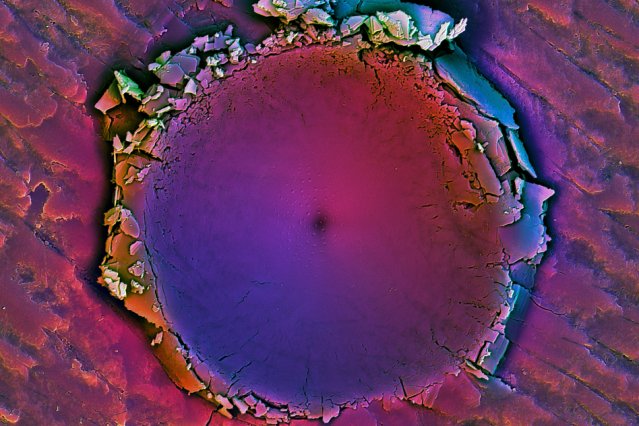
For the unique silk-based codes, Marelli says, “eventually we found a way to add a color to these microparticles [emphasis mine] so that they assemble in random structures.” The resulting unique patterns can be read out not only by a spectrograph or a portable microscope, but even by an ordinary cellphone camera with a macro lens. This image can be processed locally to generate the PUF code and then sent to the cloud and compared with a secure database to ensure the authenticity of the product. “It’s random so that people cannot easily replicate it,” says Sun. “People cannot predict it without measuring it.”

And the number of possible permutations that could result from the way they mix four basic types of colored silk nanoparticles [emphasis mine] is astronomical. “We were able to show that with a minimal amount of silk, we were able to generate 128 random bits of security,” Maji says. “So this gives rise to 2 to the power 128 possible combinations, which is extremely difficult to crack given the computational capabilities of the state-of-the-art computing systems.”

Marelli says that “for us, it’s a good test bed in order to think out-of-the-box, and how we can have a path that somehow is more democratic.” In this case, that means “something that you can literally read with your phone, and you can fabricate by simply drop casting a solution, without using any advanced manufacturing technique, without going in a clean room.”

Some additional work will be needed to make this a practical commercial product, Chandrakasan says. “There will have to be a development for at-scale reading” via smartphones. “So. that’s clearly a future opportunity.” But the principle now shows a clear path to the day when “a farmer could at least, maybe not every seed, but could maybe take some random seeds in a particular batch and verify them,” he says.

I’ve looked at the paper (very quickly) and haven’t spotted any mention of silk nanoparticles. It’s all silk microparticles.

Here’s a link to and a citation for the paper,

Integrating biopolymer design with physical unclonable functions for anticounterfeiting and product traceability in agriculture by Hui Sun, Saurav Maji, Anantha P. Chandrakasan, and Benedetto Marelli. Science Advances 22 Mar 2023 Vol 9, Issue 12 DOI: 10.1126/sciadv.adf1978

This paper is open access.

Scaling graphene production up to industrial strength

If graphene is going to be a ubiquitous material in the future, production methods need to change. An Aug. 7, 2015 news item on Nanowerk announces a new technique to achieve that goal,

Producing graphene in bulk is critical when it comes to the industrial exploitation of this exceptional two-dimensional material. To that end, [European Commission] Graphene Flagship researchers have developed a novel variant on the chemical vapour deposition process which yields high quality material in a scalable manner. This advance should significantly narrow the performance gap between synthetic and natural graphene.

An Aug. 7, 2015 European Commission Graphene Flagship press release by Francis Sedgemore, which originated the news item, describes the problem,

Media-friendly Nobel laureates peeling layers of graphene from bulk graphite with sticky tape may capture the public imagination, but as a manufacturing process the technique is somewhat lacking. Mechanical exfoliation may give us pristine graphene, but industry requires scalable and cost-effective production processes with much higher yields.

On to the new method (from the press release),

Flagship-affiliated physicists from RWTH Aachen University and Forschungszentrum Jülich have together with colleagues in Japan devised a method for peeling graphene flakes from a CVD substrate with the help of intermolecular forces. …

Key to the process is the strong van der Waals interaction that exists between graphene and hexagonal boron nitride, another 2d material within which it is encapsulated. The van der Waals force is the attractive sum of short-range electric dipole interactions between uncharged molecules.

Thanks to strong van der Waals interactions between graphene and boron nitride, CVD graphene can be separated from the copper and transferred to an arbitrary substrate. The process allows for re-use of the catalyst copper foil in further growth cycles, and minimises contamination of the graphene due to processing.

Raman spectroscopy and transport measurements on the graphene/boron nitride heterostructures reveals high electron mobilities comparable with those observed in similar assemblies based on exfoliated graphene. Furthermore – and this comes as something of a surprise to the researchers – no noticeable performance changes are detected between devices developed in the first and subsequent growth cycles. This confirms the copper as a recyclable resource in the graphene fabrication process.

“Chemical vapour deposition is a highly scalable and cost-efficient technology,” says Christoph Stampfer, head of the 2nd Institute of Physics A in Aachen, and co-author of the technical article. “Until now, graphene synthesised this way has been significantly lower in quality than that obtained with the scotch-tape method, especially when it comes to the material’s electronic properties. But no longer. We demonstrate a novel fabrication process based on CVD that yields ultra-high quality synthetic graphene samples. The process is in principle suitable for industrial-scale production, and narrows the gap between graphene research and its technological applications.”

With their dry-transfer process, Banszerus and his colleagues have shown that the electronic properties of CVD-grown graphene can in principle match those of ultrahigh-mobility exfoliated graphene. The key is to transfer CVD graphene from its growth substrate in such a way that chemical contamination is avoided. The high mobility of pristine graphene is thus preserved, and the approach allows for the substrate material to be recycled without degradation.

Here’s a link to and citation for the paper,

Ultrahigh-mobility graphene devices from chemical vapor deposition on reusable copper by Luca Banszerus, Michael Schmitz, Stephan Engels, Jan Dauber, Martin Oellers, Federica Haupt, Kenji Watanabe, Takashi Taniguchi, Bernd Beschoten, and Christoph Stampfer. Science Advances  31 Jul 2015: Vol. 1, no. 6, e1500222 DOI: 10.1126/sciadv.1500222

This article appears to be open access.

For those interested in finding out more about chemical vapour deposition (CVD), David Chandler has written a June 19, 2015 article for the Massachusetts Institute of Technology (MIT) titled:  Explained: chemical vapor deposition (Technique enables production of pure, uniform coatings of metals or polymers, even on contoured surfaces.)

Next supercapacitor: crumpled graphene?

An Oct. 3, 2014 news item on ScienceDaily features the use of graphene as a possible supercapacitor,

When someone crumples a sheet of paper, that usually means it’s about to be thrown away. But researchers have now found that crumpling a piece of graphene “paper” — a material formed by bonding together layers of the two-dimensional form of carbon — can actually yield new properties that could be useful for creating extremely stretchable supercapacitors to store energy for flexible electronic devices.

The finding is reported in the journal Scientific Reports by MIT’s {Massachusetts Institute of Technology] Xuanhe Zhao, an assistant professor of mechanical engineering and civil and environmental engineering, and four other authors. The new, flexible superconductors should be easy and inexpensive to fabricate, the team says.

An Oct. 3, 2014 MIT news release by David Chandler (also on EurekAlert), which originated the news item, explains the technology at more length,

“Many people are exploring graphene paper: It’s a good candidate for making supercapacitors, because of its large surface area per mass,” Zhao says. Now, he says, the development of flexible electronic devices, such as wearable or implantable biomedical sensors or monitoring devices, will require flexible power-storage systems.

Like batteries, supercapacitors can store electrical energy, but they primarily do so electrostatically, rather than chemically — meaning they can deliver their energy faster than batteries can. Now Zhao and his team have demonstrated that by crumpling a sheet of graphene paper into a chaotic mass of folds, they can make a supercapacitor that can easily be bent, folded, or stretched to as much as 800 percent of its original size. The team has made a simple supercapacitor using this method as a proof of principle.

The material can be crumpled and flattened up to 1,000 times, the team has demonstrated, without a significant loss of performance. “The graphene paper is pretty robust,” Zhao says, “and we can achieve very large deformations over multiple cycles.” Graphene, a structure of pure carbon just one atom thick with its carbon atoms arranged in a hexagonal array, is one of the strongest materials known.

To make the crumpled graphene paper, a sheet of the material was placed in a mechanical device that first compressed it in one direction, creating a series of parallel folds or pleats, and then in the other direction, leading to a chaotic, rumpled surface. When stretched, the material’s folds simply smooth themselves out.

Forming a capacitor requires two conductive layers — in this case, two sheets of crumpled graphene paper — with an insulating layer in between, which in this demonstration was made from a hydrogel material. Like the crumpled graphene, the hydrogel is highly deformable and stretchable, so the three layers remain in contact even while being flexed and pulled.

Though this initial demonstration was specifically to make a supercapacitor, the same crumpling technique could be applied to other uses, Zhao says. For example, the crumpled graphene material might be used as one electrode in a flexible battery, or could be used to make a stretchable sensor for specific chemical or biological molecules.

Here is a link to and a citation for the paper,

Stretchable and High-Performance Supercapacitors with Crumpled Graphene Papers by Jianfeng Zang, Changyong Cao, Yaying Feng, Jie Liu, & Xuanhe Zhao. Scientific Reports 4, Article number: 6492 doi:10.1038/srep06492 Published 01 October 2014

This is an open access article.

ETA Oct. 8, 2014: Dexter Johnson of the Nanoclast blog on the IEEE (Institute of Electrical and Electronics Engineers) website has an Oct. 7, 2014 post where he comments about the ‘flexibility’ aspect of this work.

Things falling apart: both a Nigerian novel and research at the Massachusetts Intitute of Technology

First the Nigerian novel ‘Things Fall Apart‘ (from its Wikipedia entry; Note: Links have been removed),

Things Fall Apart is an English-language novel by Nigerian author Chinua Achebe published in 1958 by William Heinemann Ltd in the UK; in 1962, it was also the first work published in Heinemann’s African Writers Series. Things Fall Apart is seen as the archetypal modern African novel in English, one of the first to receive global critical acclaim. It is a staple book in schools throughout Africa and is widely read and studied in English-speaking countries around the world. The title of the novel comes from William Butler Yeats’ poem “The Second Coming”.[1]

For those unfamiliar with the Yeats poem, this is the relevant passage (from Wikipedia entry for The Second Coming),

Turning and turning in the widening gyre
The falcon cannot hear the falconer;
Things fall apart; the centre cannot hold;
Mere anarchy is loosed upon the world,
The blood-dimmed tide is loosed, and everywhere
The ceremony of innocence is drowned;
The best lack all conviction, while the worst
Are full of passionate intensity.

The other ‘Things fall apart’ item, although it’s an investigation into ‘how things fall apart’, is mentioned in an Aug. 4, 2014 news item on Nanowerk,

Materials that are firmly bonded together with epoxy and other tough adhesives are ubiquitous in modern life — from crowns on teeth to modern composites used in construction. Yet it has proved remarkably difficult to study how these bonds fracture and fail, and how to make them more resistant to such failures.

Now researchers at MIT [Massachusetts Institute of Technology] have found a way to study these bonding failures directly, revealing the crucial role of moisture in setting the stage for failure. Their findings are published in the journal Proceedings of the National Academy of Science in a paper by MIT professors of civil and environmental engineering Oral Buyukozturk and Markus Buehler; research associate Kurt Broderick of MIT’s Microsystems Technology Laboratories; and doctoral student Denvid Lau, who has since joined the faculty at the City University of Hong Kong.

An Aug. 4, 2014 MIT news release written by David Chandler (also on EurekAlert), which originated the news item, provides an unexpectedly fascinating discussion of bonding, interfaces, and infrastructure,

“The bonding problem is a general problem that is encountered in many disciplines, especially in medicine and dentistry,” says Buyukozturk, whose research has focused on infrastructure, where such problems are also of great importance. “The interface between a base material and epoxy, for example, really controls the properties. If the interface is weak, you lose the entire system.”

“The composite may be made of a strong and durable material bonded to another strong and durable material,” Buyukozturk adds, “but where you bond them doesn’t necessarily have to be strong and durable.”

Besides dental implants and joint replacements, such bonding is also critical in construction materials such as fiber-reinforced polymers and reinforced concrete. But while such materials are widespread, understanding how they fail is not simple.

There are standard methods for testing the strength of materials and how they may fail structurally, but bonded surfaces are more difficult to model. “When we are concerned with deterioration of this interface when it is degraded by moisture, classical methods can’t handle that,” Buyukozturk says. “The way to approach it is to look at the molecular level.”

When such systems are exposed to moisture, “it initiates new molecules at the interface,” Buyukozturk says, “and that interferes with the bonding mechanism. How do you assess how weak the interface becomes when it is affected? We came up with an innovative method to assess the interface weakening as a result of exposure to environmental effects.”

The team used a combination of molecular simulations and laboratory tests in its assessment. The modeling was based on fundamental principles of molecular interactions, not on empirical data, Buyukozturk says.

In the laboratory tests, Buyukozturk and his colleagues controlled the residual stresses in a metal layer that was bonded and then forcibly removed. “We validated the method, and showed that moisture has a degrading effect,” he says.

The findings could lead to exploration of new ways to prevent moisture from reaching into the bonded layer, perhaps using better sealants. “Moisture is the No. 1 enemy,” Buyukozturk says.

“I think this is going to be an important step toward assessment of the bonding, and enable us to design more durable composites,” he adds. “It gives a quantitative knowledge of the interface” — for example, predicting that under specific conditions, a given bonded material will lose 30 percent of its strength.

Interface problems are universal, Buyukozturk says, occurring in many areas besides biomedicine and construction. “They occur in mechanical devices, in aircraft, electrical equipment, in the packaging of electronic components,” he says. “We feel this will have very broad applications.”

Bonded composite materials are beginning to be widely used in airplane manufacturing; often these composites are then bonded to traditional materials, like aluminum. “We have not had enough experience to prove the durability of these composite systems is going to be there after 20 years,” Buyukozturk says.

Here’s a link to and a citation for the research paper,

A robust nanoscale experimental quantification of fracture energy in a bilayer material system by Denvid Lau, Kurt Broderick, Markus J. Buehler, and Oral Büyüköztürk. PNAS, doi: 10.1073/pnas.1402893111 published August 5, 2014

This paper is behind a paywall.

Bioceramic armour: tough and clear

This story about a mollusk and its armour eventually led me back to one of my favourite science writers, David L. Chandler at the Massachusetts Institute of Technology (MIT). First, here’s an excerpt from a March 30, 2014 news item on ScienceDaily,

The shells of a sea creature, the mollusk Placuna placenta, are not only exceptionally tough, but also clear enough to read through. Now, researchers at MIT have analyzed these shells to determine exactly why they are so resistant to penetration and damage — even though they are 99 percent calcite, a weak, brittle mineral.

The shells’ unique properties emerge from a specialized nanostructure that allows optical clarity, as well as efficient energy dissipation and the ability to localize deformation, the researchers found. The results are published this week in the journal Nature Materials, in a paper co-authored by MIT graduate student Ling Li and professor Christine Ortiz.

A March 30, 2014 MIT press release (I’m not positive Chandler wrote this but he is the press contact) describes both the engineered bioceramic armour and the mollusk’s naturally occurring armour,

Engineered ceramic-based armor, while designed to resist penetration, often lacks the ability to withstand multiple blows, due to large-scale deformation and fracture that can compromise its structural integrity, Ortiz says. In transparent armor systems, such deformation can also obscure visibility.

Creatures that have evolved natural exoskeletons — many of them ceramic-based — have developed ingenious designs that can withstand multiple penetrating attacks from predators. The shells of a few species, such as Placuna placenta, are also optically clear.

To test exactly how the shells — which combine calcite with about 1 percent organic material — respond to penetration, the researchers subjected samples to indentation tests, using a sharp diamond tip in an experimental setup that could measure loads precisely. They then used high-resolution analysis methods, such as electron microscopy and diffraction, to examine the resulting damage.

The material initially isolates damage through an atomic-level process called “twinning” within the individual ceramic building blocks: A crystal breaks up into a pair of mirror-image regions that share a common boundary, rather like a butterfly’s wings. This twinning process occurs all around the stressed region, helping to form a kind of boundary that keeps the damage from spreading outward.

The MIT researchers found that twinning then activates “a series of additional energy-dissipation mechanisms … which preserve the mechanical and optical integrity of the surrounding material,” Li says. This produces a material that is 10 times more efficient in dissipating energy than the pure mineral, Li adds.

The properties of this natural armor make it a promising template for the development of bio-inspired synthetic materials for both commercial and military applications — such as eye and face protection for soldiers, windows and windshields, and blast shields, Ortiz says.

Huajian Gao, a professor of engineering at Brown University who was not involved in this research, calls it “an excellent and elegant piece of work.” He says it “successfully demonstrates the effectiveness of nanoscale deformation twins in energy dissipation in bioceramics, and should be able to inspire and guide the development of manmade ceramic materials.” He adds, “As a first-of-its-kind [demonstration of] the effectiveness of deformation twins in natural materials, this work should have huge practical impact.”

The work was supported by the National Science Foundation; the U.S. Army Research Office through the MIT Institute for Soldier Nanotechnologies; the National Security Science and Engineering Faculty Fellowships Program; and the Office of the Assistant Secretary of Defense for Research and Engineering.

The researchers have produced an image showing how the mollusk shell reacts to being damaged,

A Scanning Electron Microscope (SEM) image of the region surrounding an indentation the researchers made in a piece of shell from Placuna placenta. The image shows the localization of damage to the area immediately surrounding the stress. Image: Ling Li and James C. Weaver. Courtesy: MIT

A Scanning Electron Microscope (SEM) image of the region surrounding an indentation the researchers made in a piece of shell from Placuna placenta. The image shows the localization of damage to the area immediately surrounding the stress.
Image: Ling Li and James C. Weaver. Courtesy: MIT

Here’s a link to and a citation for the paper,

Pervasive nanoscale deformation twinning as a catalyst for efficient energy dissipation in a bioceramic armour by Ling Li & Christine Ortiz. Nature Materials (2014) doi:10.1038/nmat3920 Published online 30 March 2014

This paper is behind a paywall.

Water desalination by graphene and water purification by sapwood

I have two items about water. The first concerns a new technique from MIT (Massachusetts Institute of Technology) for desalination using graphene and sapwood, respectively*. From a Feb. 25, 2014 news release by David Chandler on EurekAlert,

Researchers have devised a way of making tiny holes of controllable size in sheets of graphene, a development that could lead to ultrathin filters for improved desalination or water purification.

The team of researchers at MIT, Oak Ridge National Laboratory, and in Saudi Arabia succeeded in creating subnanoscale pores in a sheet of the one-atom-thick material, which is one of the strongest materials known. …

The concept of using graphene, perforated by nanoscale pores, as a filter in desalination has been proposed and analyzed by other MIT researchers. The new work, led by graduate student Sean O’Hern and associate professor of mechanical engineering Rohit Karnik, is the first step toward actual production of such a graphene filter.

Making these minuscule holes in graphene — a hexagonal array of carbon atoms, like atomic-scale chicken wire — occurs in a two-stage process. First, the graphene is bombarded with gallium ions, which disrupt the carbon bonds. Then, the graphene is etched with an oxidizing solution that reacts strongly with the disrupted bonds — producing a hole at each spot where the gallium ions struck. By controlling how long the graphene sheet is left in the oxidizing solution, the MIT researchers can control the average size of the pores.

A big limitation in existing nanofiltration and reverse-osmosis desalination plants, which use filters to separate salt from seawater, is their low permeability: Water flows very slowly through them. The graphene filters, being much thinner, yet very strong, can sustain a much higher flow. “We’ve developed the first membrane that consists of a high density of subnanometer-scale pores in an atomically thin, single sheet of graphene,” O’Hern says.

For efficient desalination, a membrane must demonstrate “a high rejection rate of salt, yet a high flow rate of water,” he adds. One way of doing that is decreasing the membrane’s thickness, but this quickly renders conventional polymer-based membranes too weak to sustain the water pressure, or too ineffective at rejecting salt, he explains.

With graphene membranes, it becomes simply a matter of controlling the size of the pores, making them “larger than water molecules, but smaller than everything else,” O’Hern says — whether salt, impurities, or particular kinds of biochemical molecules.

The permeability of such graphene filters, according to computer simulations, could be 50 times greater than that of conventional membranes, as demonstrated earlier by a team of MIT researchers led by graduate student David Cohen-Tanugi of the Department of Materials Science and Engineering. But producing such filters with controlled pore sizes has remained a challenge. The new work, O’Hern says, demonstrates a method for actually producing such material with dense concentrations of nanometer-scale holes over large areas.

“We bombard the graphene with gallium ions at high energy,” O’Hern says. “That creates defects in the graphene structure, and these defects are more chemically reactive.” When the material is bathed in a reactive oxidant solution, the oxidant “preferentially attacks the defects,” and etches away many holes of roughly similar size. O’Hern and his co-authors were able to produce a membrane with 5 trillion pores per square centimeter, well suited to use for filtration. “To better understand how small and dense these graphene pores are, if our graphene membrane were to be magnified about a million times, the pores would be less than 1 millimeter in size, spaced about 4 millimeters apart, and span over 38 square miles, an area roughly half the size of Boston,” O’Hern says.

With this technique, the researchers were able to control the filtration properties of a single, centimeter-sized sheet of graphene: Without etching, no salt flowed through the defects formed by gallium ions. With just a little etching, the membranes started allowing positive salt ions to flow through. With further etching, the membranes allowed both positive and negative salt ions to flow through, but blocked the flow of larger organic molecules. With even more etching, the pores were large enough to allow everything to go through.

Scaling up the process to produce useful sheets of the permeable graphene, while maintaining control over the pore sizes, will require further research, O’Hern says.

Karnik says that such membranes, depending on their pore size, could find various applications. Desalination and nanofiltration may be the most demanding, since the membranes required for these plants would be very large. But for other purposes, such as selective filtration of molecules — for example, removal of unreacted reagents from DNA — even the very small filters produced so far might be useful.

“For biofiltration, size or cost are not as critical,” Karnik says. “For those applications, the current scale is suitable.”

Dexter Johnson in a Feb. 26,2014 posting provides some context for and insight into the work (from the Nanoclast blog on the IEEE [Institute of Electrical and Electronics Engineers]), Note: Links have been removed,

About 18 months ago, I wrote about an MIT project in which computer models demonstrated that graphene could act as a filter in the desalination of water through the reverse osmosis (RO) method. RO is slightly less energy intensive than the predominantly used multi-stage-flash process. The hope was that the nanopores of the graphene material would make the RO method even less energy intensive than current versions by making it easier to push the water through the filter membrane.

The models were promising, but other researchers in the field said at the time it was going to be a long road to translate a computer model to a real product.

It would seem that the MIT researchers agreed it was worth the effort and accepted the challenge to go from computer model to a real device as they announced this week that they had developed a method for creating selective pores in graphene that make it suitable for water desalination.

Here’s a link to and a citation for the paper,

Selective Ionic Transport through Tunable Subnanometer Pores in Single-Layer Graphene Membranes by Sean C. O’Hern, Michael S. H. Boutilier, Juan-Carlos Idrobo, Yi Song, Jing Kong, Tahar Laoui, Muataz Atieh, and Rohit Karnik. Nano Lett., Article ASAP DOI: 10.1021/nl404118f Publication Date (Web): February 3, 2014

Copyright © 2014 American Chemical Society

This article is behind a paywall.

The second item is also from MIT and concerns a low-tech means of purifying water. From a Feb. 27, 2014 news item on Azonano,

If you’ve run out of drinking water during a lakeside camping trip, there’s a simple solution: Break off a branch from the nearest pine tree, peel away the bark, and slowly pour lake water through the stick. The improvised filter should trap any bacteria, producing fresh, uncontaminated water.

In fact, an MIT team has discovered that this low-tech filtration system can produce up to four liters of drinking water a day — enough to quench the thirst of a typical person.

In a paper published this week in the journal PLoS ONE, the researchers demonstrate that a small piece of sapwood can filter out more than 99 percent of the bacteria E. coli from water. They say the size of the pores in sapwood — which contains xylem tissue evolved to transport sap up the length of a tree — also allows water through while blocking most types of bacteria.

Co-author Rohit Karnik, an associate professor of mechanical engineering at MIT, says sapwood is a promising, low-cost, and efficient material for water filtration, particularly for rural communities where more advanced filtration systems are not readily accessible.

“Today’s filtration membranes have nanoscale pores that are not something you can manufacture in a garage very easily,” Karnik says. “The idea here is that we don’t need to fabricate a membrane, because it’s easily available. You can just take a piece of wood and make a filter out of it.”

The Feb. 26, 2014 news release on EurekAlert, which originated the news item, describes current filtration techniques and the advantages associated with this new low-tech approach,

There are a number of water-purification technologies on the market today, although many come with drawbacks: Systems that rely on chlorine treatment work well at large scales, but are expensive. Boiling water to remove contaminants requires a great deal of fuel to heat the water. Membrane-based filters, while able to remove microbes, are expensive, require a pump, and can become easily clogged.

Sapwood may offer a low-cost, small-scale alternative. The wood is comprised of xylem, porous tissue that conducts sap from a tree’s roots to its crown through a system of vessels and pores. Each vessel wall is pockmarked with tiny pores called pit membranes, through which sap can essentially hopscotch, flowing from one vessel to another as it feeds structures along a tree’s length. The pores also limit cavitation, a process by which air bubbles can grow and spread in xylem, eventually killing a tree. The xylem’s tiny pores can trap bubbles, preventing them from spreading in the wood.

“Plants have had to figure out how to filter out bubbles but allow easy flow of sap,” Karnik observes. “It’s the same problem with water filtration where we want to filter out microbes but maintain a high flow rate. So it’s a nice coincidence that the problems are similar.”

The news release also describes the experimental procedure the scientists followed (from the news release),

To study sapwood’s water-filtering potential, the researchers collected branches of white pine and stripped off the outer bark. They cut small sections of sapwood measuring about an inch long and half an inch wide, and mounted each in plastic tubing, sealed with epoxy and secured with clamps.

Before experimenting with contaminated water, the group used water mixed with red ink particles ranging from 70 to 500 nanometers in size. After all the liquid passed through, the researchers sliced the sapwood in half lengthwise, and observed that much of the red dye was contained within the very top layers of the wood, while the filtrate, or filtered water, was clear. This experiment showed that sapwood is naturally able to filter out particles bigger than about 70 nanometers.

However, in another experiment, the team found that sapwood was unable to separate out 20-nanometer particles from water, suggesting that there is a limit to the size of particles coniferous sapwood can filter.

Finally, the team flowed inactivated, E. coli-contaminated water through the wood filter. When they examined the xylem under a fluorescent microscope, they saw that bacteria had accumulated around pit membranes in the first few millimeters of the wood. Counting the bacterial cells in the filtered water, the researchers found that the sapwood was able to filter out more than 99 percent of E. coli from water.

Karnik says sapwood likely can filter most types of bacteria, the smallest of which measure about 200 nanometers. However, the filter probably cannot trap most viruses, which are much smaller in size.

The researchers have future plans (from the news release),

Karnik says his group now plans to evaluate the filtering potential of other types of sapwood. In general, flowering trees have smaller pores than coniferous trees, suggesting that they may be able to filter out even smaller particles. However, vessels in flowering trees tend to be much longer, which may be less practical for designing a compact water filter.

Designers interested in using sapwood as a filtering material will also have to find ways to keep the wood damp, or to dry it while retaining the xylem function. In other experiments with dried sapwood, Karnik found that water either did not flow through well, or flowed through cracks, but did not filter out contaminants.

“There’s huge variation between plants,” Karnik says. “There could be much better plants out there that are suitable for this process. Ideally, a filter would be a thin slice of wood you could use for a few days, then throw it away and replace at almost no cost. It’s orders of magnitude cheaper than the high-end membranes on the market today.”

Here’s a link to and a citation for the paper,

Water Filtration Using Plant Xylem by Michael S. H. Boutilier, Jongho Lee, Valerie Chambers, Varsha Venkatesh, & Rohit Karnik. PLOS One Published: February 26, 2014 DOI: 10.1371/journal.pone.0089934

This paper is open access.

One final observation, two of the researchers (Michael S. H. Boutilier & Rohit Karnik) listed as authors on the graphene/water desalination paper are also listed on the low-tech sapwood paper solution.*

* The first sentence of the this post originally stated both items were graphene-related, it has been changed to say 1… using graphene and sapwood, respectively*’ on May 8, 2015.

The last sentence of this post was changed from

‘One final observation, two of the researchers listed as authors on the graphene/water desalination paper are also listed on the low-tech sapwood paper (Michael S. H. Boutilier & Rohit Karnik).’

to this

‘One final observation, two of the researchers (Michael S. H. Boutilier & Rohit Karnik) listed as authors on the graphene/water desalination paper are also listed on the low-tech sapwood paper solution.*’ for clarity on May 8, 2015.

Biology and lithium-air batteries

Firstly, the biology in question is that of viruses and, secondly, research in lithium-air batteries has elicited big interest according to David Chandler’s November 13, 2013 Massachusetts Institute of Technology (MIT) news piece (also on EurekAlert and Nanowerk),

Lithium-air batteries have become a hot research area in recent years: They hold the promise of drastically increasing power per battery weight, which could lead, for example, to electric cars with a much greater driving range. But bringing that promise to reality has faced a number of challenges, ….

Now, MIT researchers have found that adding genetically modified viruses to the production of nanowires — wires that are about the width of a red blood cell, and which can serve as one of a battery’s electrodes — could help solve some of these problems.

Lithium-air batteries can also be referred to as lithiium-oxygen batteries, although Chandler does not choose to mix terms as he goes on to describe the process the researchers developed,

The researchers produced an array of nanowires, each about 80 nanometers across, using a genetically modified virus called M13, which can capture molecules of metals from water and bind them into structural shapes. In this case, wires of manganese oxide — a “favorite material” for a lithium-air battery’s cathode, Belcher says — were actually made by the viruses. But unlike wires “grown” through conventional chemical methods, these virus-built nanowires have a rough, spiky surface, which dramatically increases their surface area.

Belcher, the W.M. Keck Professor of Energy and a member of MIT’s Koch Institute for Integrative Cancer Research, explains that this process of biosynthesis is “really similar to how an abalone grows its shell” — in that case, by collecting calcium from seawater and depositing it into a solid, linked structure.

The increase in surface area produced by this method can provide “a big advantage,” Belcher says, in lithium-air batteries’ rate of charging and discharging. But the process also has other potential advantages, she says: Unlike conventional fabrication methods, which involve energy-intensive high temperatures and hazardous chemicals, this process can be carried out at room temperature using a water-based process.

Also, rather than isolated wires, the viruses naturally produce a three-dimensional structure of cross-linked wires, which provides greater stability for an electrode.

A final part of the process is the addition of a small amount of a metal, such as palladium, which greatly increases the electrical conductivity of the nanowires and allows them to catalyze reactions that take place during charging and discharging. Other groups have tried to produce such batteries using pure or highly concentrated metals as the electrodes, but this new process drastically lowers how much of the expensive material is needed.

Altogether, these modifications have the potential to produce a battery that could provide two to three times greater energy density — the amount of energy that can be stored for a given weight — than today’s best lithium-ion batteries, a closely related technology that is today’s top contender, the researchers say.

MIT has produced a video highlighting the researchers’ work (this runs longer than most of the materials I embed here at approximately 11 mins. 25 secs.),

For those who want to know more about this intriguing and speculative work,

Biologically enhanced cathode design for improved capacity and cycle life for lithium-oxygen batteries by Dahyun Oh, Jifa Qi, Yi-Chun Lu, Yong Zhang, Yang Shao-Horn, & Angela M. Belcher. Nature Communications 4, Article number: 2756 doi:10.1038/ncomms3756 Published 13 November 2013

This article is behind a paywall.

ETA Nov. 15, 2013: Dexter Johnson offers more context and information, including commercialization issues, about lithium-air batteries and lithium-ion batteries in his Nov. 14, 2013 posting on the Nanoclast blog (on the IEEE [Institute of Electrical and Electronics Engineers] website).

Hydrophobic and hydrophilic for beginners

Anyone who’s interested in biomimicry (mimicking nature, for one reason or another) is likely to come across the terms hydrophobic (e.g. lotus leaves where water beads up into little balls) and hydrophilic, materials where water spreads itself evenly (e.g. desert beetles such as the stenocara are partly hydrophilic).  David L. Chandler at MIT (Massachusetts Institute of Technology) has written a good explanation (H/T phys.org) of these two states and the surface tensions which cause them in his article, Explained: Hydrophobic and hydrophilic; Better understanding of how surfaces attract or repel water could improve everything from power plants to ketchup bottles of July 16, 2013,

Materials with a special affinity for water — those it spreads across, maximizing contact — are known as hydrophilic. Those that naturally repel water, causing droplets to form, are known as hydrophobic. Both classes of materials can have a significant impact on the performance of power plants, electronics, airplane wings and desalination plants, among other technologies, says Kripa Varanasi, an associate professor of mechanical engineering at MIT. Improvements in hydrophilic and hydrophobic surfaces could provide ketchup bottles where the condiment just glides right out, glasses that never fog up, or power plants that wring more electricity from a given amount of fuel.

Hydrophilic and hydrophobic materials are defined by the geometry of water on a flat surface — specifically, the angle between a droplet’s edge and the surface underneath it. This is called the contact angle.

If the droplet spreads, wetting a large area of the surface, then the contact angle is less than 90 degrees and that surface is considered hydrophilic, or water-loving (from the Greek words for water, hydro, and love, philos). But if the droplet forms a sphere that barely touches the surface — like drops of water on a hot griddle — the contact angle is more than 90 degrees, and the surface is hydrophobic, or water-fearing.

I recommend  reading this piece in its entirety if you want find out more about this unexpectedly interesting topic. For those who don’t have the patience to read the whole article or like to augment their reading with videos, there’s the Bouncing Droplets: Superhydrophobic and Superhydrophilic Surfaces video at the Khan Academy. This well-paced  video was produced by MIT’s Bioinstrumentation Laboratory and is suitable for older children and adults.

Beginner’s guide to carbon nanotubes and nanowires

There’s a very nice Apr. 11, 2013  introductory article by David L. Chandler for the Massachusetts Institute of Technology (MIT) news office) about carbon and other nanotubes and nanowires,

The initial discovery of carbon nanotubes — tiny tubes of pure carbon, essentially sheets of graphene rolled up unto a cylinder — is generally credited to a paper published in 1991 by the Japanese physicist Sumio Ijima (although some forms of carbon nanotubes had been observed earlier). Almost immediately, there was an explosion of interest in this exotic form of a commonplace material. Nanowires — solid crystalline fibers, rather than hollow tubes — gained similar prominence a few years later.

Due to their extreme slenderness, both nanotubes and nanowires are essentially one-dimensional. “They are quasi-one-dimensional materials,” says MIT associate professor of materials science and engineering Silvija Gradečak: “Two of their dimensions are on the nanometer scale.” This one-dimensionality confers distinctive electrical and optical properties.

For one thing, it means that the electrons and photons within these nanowires experience “quantum confinement effects,” Gradečak says. And yet, unlike other materials that produce such quantum effects, such as quantum dots, nanowires’ length makes it possible for them to connect with other macroscopic devices and the outside world.

The structure of a nanowire is so simple that there’s no room for defects, and electrons pass through unimpeded, Gradečak explains. This sidesteps a major problem with typical crystalline semiconductors, such as those made from a wafer of silicon: There are always defects in those structures, and those defects interfere with the passage of electrons.

H/T Nanowerk Apr. 11, 2013 news item. There’s more to read at the MIT website and I recommend this as a good beginner’s piece since the focus is entirely on what carbon nanotubes and nanowires are , how they are formed, and which distinctive properties are theirs. You can find some of this information in the odd paragraph of a news release touting the latest research but I’m very excited to find this much explanatory material in one place.

Another very good explanatory piece, this one focused on carbon nanotubes and risk, is a video produced by Dr. Andrew Maynard for his Risk Bites series. I featured and embedded it in my Mar. 15, 2013 posting. titled, The long, the short, the straight, and the curved of them: all about carbon nanotubes.  You can also find the video in Andrew’s Mar. 14, 2013 posting on his 2020 Science blog where he also writes about the then recently released information from the US National Institute of Occupational Health and Safety on carbon nanotubes and toxicity.

Adventures in time, mass, and topological insulators

Nano at a billionth (of a second, or a metre, or some other measure) is not the smallest unit of measurement, despite how we often talk about nano ‘anything’. But, as we continue to explore matter at ever more subtle levels, we need ever smaller units of measure and there are some ready for use.

I have a few excerpts from a Sept. 18, 2012  article (Explained: Femtoseconds and attoseconds) by David Chandler at the Massachusetts Institute of Technology (MIT) describing some of these smaller units of measure and how they were devised,

Back in the first half of the 20th century, when MIT’s famed Harold “Doc” Edgerton was perfecting his system for capturing fast-moving events on film, the ability to observe changes unfolding at a scale of microseconds — millionths of a second — was considered a remarkable achievement. This led to now-famous images such as one of a bullet piercing an apple, captured in midflight.

Nowadays, microsecond-resolution imagery is almost ho-hum. The cutting edge of research passed through nanoseconds (billionths of a second) and picoseconds (trillionths) in the 1970s and 1980s. Today, researchers can easily reach into the realm of femtoseconds — quadrillionths (or millionths of a billionth) of a second, the timescale of motions within molecules.

Femtosecond laser research led to the development, in 2000, of a system that revolutionized the measurement of optical frequencies and enabled optical clocks. Continuing the progress, today’s top-shelf technologies are beginning to make it possible to observe events that last less than 100 attoseconds, or quintillionths of a second.

Those prefixes — micro, nano, pico, femto and atto — are part of an internationally agreed-upon system called SI units (from the French Système International d’Unités, or International System of Units). The system was officially adopted in 1960, and has been updated periodically, most recently in 1991. It encompasses a total of 20 prefixes, 10 of them for decimal amounts, and 10 more for large multiples of the basic units (mega, giga, tera and so on).

As Chandler points out in more detail than I have, there’s a reason for developing these units of measure,

The ability to observe events on such timescales is important for basic physics — to understand how atoms move within molecules — as well as for engineering semiconductor devices, and for understanding basic biological processes at the molecular level.

But physicists and engineers are interested in pushing these limits ever further. To understand the movements of electrons, and eventually those of subatomic particles, requires attaining the attosecond and ultimately zeptosecond (sextillionths of a second) range, Kaertner says. Achieving that requires pushing technology to produce pulses using higher-wavelength sources, and also producing pulses that encompass a wider range of frequencies — a more broadband source.

I finally managed to conceptualize the nanoscale a few years ago but it appears I have more work to do. Chandler offers some suggestions for imagining the femtoscale,

So, just how short is a femtosecond? One way to think of it, Kaertner [Franz Kaertner, MIT adjunct professor of electrical engineering] says, is in terms of how far light can move in a given amount of time. Light travels about 300,000 kilometers (or 186,000 miles) in one second. That means it goes about 30 centimeters — about one foot — in one nanosecond. In one femtosecond, light travels just 300 nanometers — about the size of the biggest particle that can pass through a HEPA filter, and just slightly larger than the smallest bacteria.

Another way of thinking about the length of a femtosecond is this: One femtosecond is to one second as one second is to about 32 million years.

Chandler discuses in another MIT article (Watching electrons move at high speed) also posted on Sept. 18, 2012, a new electronic material, a topological insulator, and the importance of viewing the behaviour of electrons present in such an insulator,

Topological insulators are exotic materials, discovered just a few years ago, that hold great promise for new kinds of electronic devices. The unusual behavior of electrons within them has been very difficult to study, but new techniques developed by a team of researchers at MIT could help unlock the mysteries of exactly how electrons move and react in these materials, opening up new possibilities for harnessing them.

For the first time, the MIT team has managed to create three-dimensional “movies” of electron behavior in a topological insulator, or TI. [can be viewed here] The movies can capture vanishingly small increments of time — down to the level of a few femtoseconds, or millionths of a billionth of a second — so that they can catch the motions of electrons as they scatter in response to a very short pulse of light.

Electrons normally have mass, just like many other fundamental particles, but when moving along the surface of TIs they move as if they were massless, like light — one of the extraordinary characteristics that give these new materials such promise for new technologies. [emphases mine]

It’s the bit about mass and masslessness that caught my eye. Fascincating, non? Here’s a graphical representation of what the MIT scientists observed (I think it looks like a cup or a grail),

Three-dimensional graphical representations of the way electrons respond to an input of energy, delivered by a pulse of laser light. The horizontal axis represents the electrons’ momentum, and the vertical axis shows their energy. The time sequence runs from top left to bottom right, and the laser pulse arrives just before the second image, causing a sudden burst of higher energy levels. Images courtesy of Yihua Wang and Nuh Gedik [of MIT]

Here’s a bit more about TIs and possible future applications,

TIs are a class of materials with seemingly contradictory characteristics: The bulk of the material acts as an insulator, almost completely blocking any flow of electrons. But the surface of the material behaves as a very good conductor, like a metal, allowing electrons to travel freely. In fact, the surface is even more conductive than normal metals — allowing electrons to travel at almost the speed of light and to be unaffected by impurities in the material, which normally hinder their motion.

Because of these characteristics, TIs are seen as a promising new material for electronic circuits and data-storage devices. But developing such new devices requires a better understanding of exactly how electrons move around on and inside the TI, and how the surface electrons interact with those inside the material.

I highly recommend reading both of Chandler’s articles.