Tag Archives: Dexter Johnson

IBM and a 5 nanometre chip

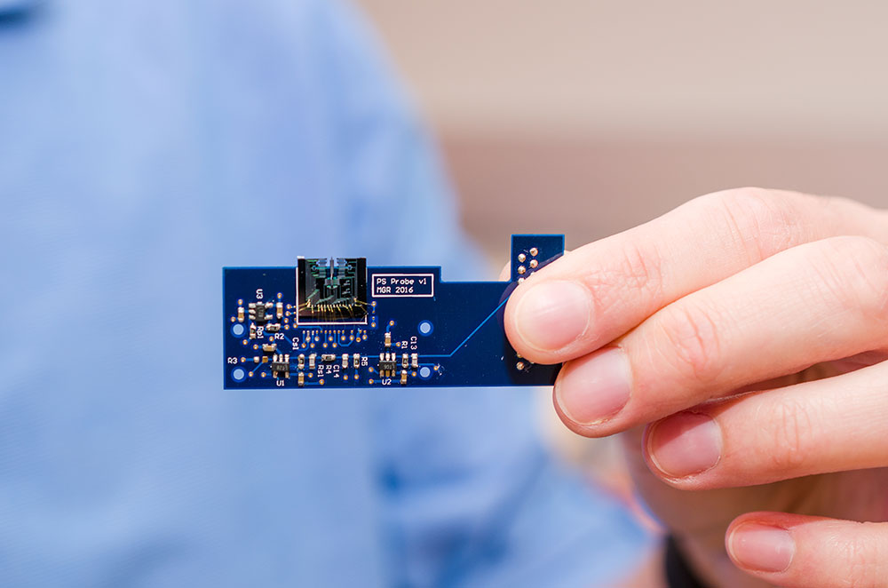
If this continues, they’re going to have change the scale from nano to pico. IBM has announced work on a 5 nanometre (5nm) chip in a June 5, 2017 news item on Nanotechnology Now,

IBM (NYSE: IBM), its Research Alliance partners GLOBALFOUNDRIES and Samsung, and equipment suppliers have developed an industry-first process to build silicon nanosheet transistors that will enable 5 nanometer (nm) chips. The details of the process will be presented at the 2017 Symposia on VLSI Technology and Circuits conference in Kyoto, Japan. In less than two years since developing a 7nm test node chip with 20 billion transistors, scientists have paved the way for 30 billion switches on a fingernail-sized chip.

A June 5, 2017 IBM news release, which originated the news item, spells out some of the details about IBM’s latest breakthrough,

The resulting increase in performance will help accelerate cognitive computing [emphasis mine], the Internet of Things (IoT), and other data-intensive applications delivered in the cloud. The power savings could also mean that the batteries in smartphones and other mobile products could last two to three times longer than today’s devices, before needing to be charged.

Scientists working as part of the IBM-led Research Alliance at the SUNY Polytechnic Institute Colleges of Nanoscale Science and Engineering’s NanoTech Complex in Albany, NY achieved the breakthrough by using stacks of silicon nanosheets as the device structure of the transistor, instead of the standard FinFET architecture, which is the blueprint for the semiconductor industry up through 7nm node technology.

“For business and society to meet the demands of cognitive and cloud computing in the coming years, advancement in semiconductor technology is essential,” said Arvind Krishna, senior vice president, Hybrid Cloud, and director, IBM Research. “That’s why IBM aggressively pursues new and different architectures and materials that push the limits of this industry, and brings them to market in technologies like mainframes and our cognitive systems.”

The silicon nanosheet transistor demonstration, as detailed in the Research Alliance paper Stacked Nanosheet Gate-All-Around Transistor to Enable Scaling Beyond FinFET, and published by VLSI, proves that 5nm chips are possible, more powerful, and not too far off in the future.

Compared to the leading edge 10nm technology available in the market, a nanosheet-based 5nm technology can deliver 40 percent performance enhancement at fixed power, or 75 percent power savings at matched performance. This improvement enables a significant boost to meeting the future demands of artificial intelligence (AI) systems, virtual reality and mobile devices.

Building a New Switch

“This announcement is the latest example of the world-class research that continues to emerge from our groundbreaking public-private partnership in New York,” said Gary Patton, CTO and Head of Worldwide R&D at GLOBALFOUNDRIES. “As we make progress toward commercializing 7nm in 2018 at our Fab 8 manufacturing facility, we are actively pursuing next-generation technologies at 5nm and beyond to maintain technology leadership and enable our customers to produce a smaller, faster, and more cost efficient generation of semiconductors.”

IBM Research has explored nanosheet semiconductor technology for more than 10 years. This work is the first in the industry to demonstrate the feasibility to design and fabricate stacked nanosheet devices with electrical properties superior to FinFET architecture.

This same Extreme Ultraviolet (EUV) lithography approach used to produce the 7nm test node and its 20 billion transistors was applied to the nanosheet transistor architecture. Using EUV lithography, the width of the nanosheets can be adjusted continuously, all within a single manufacturing process or chip design. This adjustability permits the fine-tuning of performance and power for specific circuits – something not possible with today’s FinFET transistor architecture production, which is limited by its current-carrying fin height. Therefore, while FinFET chips can scale to 5nm, simply reducing the amount of space between fins does not provide increased current flow for additional performance.

“Today’s announcement continues the public-private model collaboration with IBM that is energizing SUNY-Polytechnic’s, Albany’s, and New York State’s leadership and innovation in developing next generation technologies,” said Dr. Bahgat Sammakia, Interim President, SUNY Polytechnic Institute. “We believe that enabling the first 5nm transistor is a significant milestone for the entire semiconductor industry as we continue to push beyond the limitations of our current capabilities. SUNY Poly’s partnership with IBM and Empire State Development is a perfect example of how Industry, Government and Academia can successfully collaborate and have a broad and positive impact on society.”

Part of IBM’s $3 billion, five-year investment in chip R&D (announced in 2014), the proof of nanosheet architecture scaling to a 5nm node continues IBM’s legacy of historic contributions to silicon and semiconductor innovation. They include the invention or first implementation of the single cell DRAM, the Dennard Scaling Laws, chemically amplified photoresists, copper interconnect wiring, Silicon on Insulator, strained engineering, multi core microprocessors, immersion lithography, high speed SiGe, High-k gate dielectrics, embedded DRAM, 3D chip stacking and Air gap insulators.

I last wrote about IBM and computer chips in a July 15, 2015 posting regarding their 7nm chip. You may want to scroll down approximately 55% of the way where I note research from MIT (Massachusetts Institute of Technology) about metal nanoparticles with unexpected properties possibly having an impact on nanoelectronics.

Getting back to IBM, they have produced a slick video about their 5nm chip breakthrough,

Meanwhile, Katherine Bourzac provides technical detail in a June 5, 2017 posting on the Nanoclast blog (on the IEEE [Institute of Electrical and Electronics Engineers] website), Note: A link has been removed,

Researchers at IBM believe the future of the transistor is in stacked nanosheets. …

Today’s state-of-the-art transistor is the finFET, named for the fin-like ridges of current-carrying silicon that project from the chip’s surface. The silicon fins are surrounded on their three exposed sides by a structure called the gate. The gate switches the flow of current on, and prevents electrons from leaking out when the transistor is off. This design is expected to last from this year’s bleeding-edge process technology, the “10-nanometer” node, through the next node, 7 nanometers. But any smaller, and these transistors will become difficult to switch off: electrons will leak out, even with the three-sided gates.

So the semiconductor industry has been working on alternatives for the upcoming 5 nanometer node. One popular idea is to use lateral silicon nanowires that are completely surrounded by the gate, preventing electron leaks and saving power. This design is called “gate all around.” IBM’s new design is a variation on this. In their test chips, each transistor is made up of three stacked horizontal sheets of silicon, each only a few nanometers thick and completely surrounded by a gate.

Why a sheet instead of a wire? Huiming Bu, director of silicon integration and devices at IBM, says nanosheets can bring back one of the benefits of pre-finFET, planar designs. Designers used to be able to vary the width of a transistor to prioritize fast operations or energy efficiency. Varying the amount of silicon in a finFET transistor is not practicable because it would mean making some fins taller and other shorter. Fins must all be the same height due to manufacturing constraints, says Bu.

IBM’s nanosheets can range from 8 to 50 nanometers in width. “Wider gives you better performance but takes more power, smaller width relaxes performance but reduces power use,” says Bu. This will allow circuit designers to pick and choose what they need, whether they are making a power efficient mobile chip processor or designing a bank of SRAM memory. “We are bringing flexibility back to the designers,” he says.

The test chips have 30 billion transistors. …

It was a struggle trying to edit Bourzac’s posting with its good detail and clear writing. I encourage you to read it (June 5, 2017 posting) in its entirety.

As for where this drive downwards to the ‘ever smaller’ is going, there’s Dexter’s Johnson’s June 29, 2017 posting about another IBM team’s research on his Nanoclast blog on the IEEE website (Note: Links have been removed),

There have been increasing signs coming from the research community that carbon nanotubes are beginning to step up to the challenge of offering a real alternative to silicon-based complementary metal-oxide semiconductor (CMOS) transistors.

Now, researchers at IBM Thomas J. Watson Research Center have advanced carbon nanotube-based transistors another step toward meeting the demands of the International Technology Roadmap for Semiconductors (ITRS) for the next decade. The IBM researchers have fabricated a p-channel transistor based on carbon nanotubes that takes up less than half the space of leading silicon technologies while operating at a lower voltage.

In research described in the journal Science, the IBM scientists used a carbon nanotube p-channel to reduce the transistor footprint; their transistor contains all components to 40 square nanometers [emphasis mine], an ITRS roadmap benchmark for ten years out.

One of the keys to being able to reduce the transistor to such a small size is the use of the carbon nanotube as the channel in place of silicon. The nanotube is only 1 nanometer thick. Such thinness offers a significant advantage in electrostatics, so that it’s possible to reduce the device gate length to 10 nanometers without seeing the device performance adversely affected by short-channel effects. An additional benefit of the nanotubes is that the electrons travel much faster, which contributes to a higher level of device performance.

Happy reading!

Atomic force microscope (AFM) shrunk down to a dime-sized device?

Before getting to the announcement, here’s a little background from Dexter Johnson’s Feb. 21, 2017 posting on his NanoClast blog (on the IEEE [Institute of Electrical and Electronics Engineers] website; Note: Links have been removed),

Ever since the 1980s, when Gerd Binnig of IBM first heard that “beautiful noise” made by the tip of the first scanning tunneling microscope (STM) dragging across the surface of an atom, and he later developed the atomic force microscope (AFM), these microscopy tools have been the bedrock of nanotechnology research and development.

AFMs have continued to evolve over the years, and at one time, IBM even looked into using them as the basis of a memory technology in the company’s Millipede project. Despite all this development, AFMs have remained bulky and expensive devices, costing as much as $50,000 [or more].

Now, here’s the announcement in a Feb. 15, 2017 news item on Nanowerk,

Researchers at The University of Texas at Dallas have created an atomic force microscope on a chip, dramatically shrinking the size — and, hopefully, the price tag — of a high-tech device commonly used to characterize material properties.

“A standard atomic force microscope is a large, bulky instrument, with multiple control loops, electronics and amplifiers,” said Dr. Reza Moheimani, professor of mechanical engineering at UT Dallas. “We have managed to miniaturize all of the electromechanical components down onto a single small chip.”

A Feb. 15, 2017 University of Texas at Dallas news release, which originated the news item, provides more detail,

An atomic force microscope (AFM) is a scientific tool that is used to create detailed three-dimensional images of the surfaces of materials, down to the nanometer scale — that’s roughly on the scale of individual molecules.

The basic AFM design consists of a tiny cantilever, or arm, that has a sharp tip attached to one end. As the apparatus scans back and forth across the surface of a sample, or the sample moves under it, the interactive forces between the sample and the tip cause the cantilever to move up and down as the tip follows the contours of the surface. Those movements are then translated into an image.

“An AFM is a microscope that ‘sees’ a surface kind of the way a visually impaired person might, by touching. You can get a resolution that is well beyond what an optical microscope can achieve,” said Moheimani, who holds the James Von Ehr Distinguished Chair in Science and Technology in the Erik Jonsson School of Engineering and Computer Science. “It can capture features that are very, very small.”

The UT Dallas team created its prototype on-chip AFM using a microelectromechanical systems (MEMS) approach.

“A classic example of MEMS technology are the accelerometers and gyroscopes found in smartphones,” said Dr. Anthony Fowler, a research scientist in Moheimani’s Laboratory for Dynamics and Control of Nanosystems and one of the article’s co-authors. “These used to be big, expensive, mechanical devices, but using MEMS technology, accelerometers have shrunk down onto a single chip, which can be manufactured for just a few dollars apiece.”

The MEMS-based AFM is about 1 square centimeter in size, or a little smaller than a dime. It is attached to a small printed circuit board, about half the size of a credit card, which contains circuitry, sensors and other miniaturized components that control the movement and other aspects of the device.

Conventional AFMs operate in various modes. Some map out a sample’s features by maintaining a constant force as the probe tip drags across the surface, while others do so by maintaining a constant distance between the two.

“The problem with using a constant height approach is that the tip is applying varying forces on a sample all the time, which can damage a sample that is very soft,” Fowler said. “Or, if you are scanning a very hard surface, you could wear down the tip,”

The MEMS-based AFM operates in “tapping mode,” which means the cantilever and tip oscillate up and down perpendicular to the sample, and the tip alternately contacts then lifts off from the surface. As the probe moves back and forth across a sample material, a feedback loop maintains the height of that oscillation, ultimately creating an image.

“In tapping mode, as the oscillating cantilever moves across the surface topography, the amplitude of the oscillation wants to change as it interacts with sample,” said Dr. Mohammad Maroufi, a research associate in mechanical engineering and co-author of the paper. “This device creates an image by maintaining the amplitude of oscillation.”

Because conventional AFMs require lasers and other large components to operate, their use can be limited. They’re also expensive.

“An educational version can cost about $30,000 or $40,000, and a laboratory-level AFM can run $500,000 or more,” Moheimani said. “Our MEMS approach to AFM design has the potential to significantly reduce the complexity and cost of the instrument.

“One of the attractive aspects about MEMS is that you can mass produce them, building hundreds or thousands of them in one shot, so the price of each chip would only be a few dollars. As a result, you might be able to offer the whole miniature AFM system for a few thousand dollars.”

A reduced size and price tag also could expand the AFMs’ utility beyond current scientific applications.

“For example, the semiconductor industry might benefit from these small devices, in particular companies that manufacture the silicon wafers from which computer chips are made,” Moheimani said. “With our technology, you might have an array of AFMs to characterize the wafer’s surface to find micro-faults before the product is shipped out.”

The lab prototype is a first-generation device, Moheimani said, and the group is already working on ways to improve and streamline the fabrication of the device.

“This is one of those technologies where, as they say, ‘If you build it, they will come.’ We anticipate finding many applications as the technology matures,” Moheimani said.

In addition to the UT Dallas researchers, Michael Ruppert, a visiting graduate student from the University of Newcastle in Australia, was a co-author of the journal article. Moheimani was Ruppert’s doctoral advisor.

So, an AFM that could cost as much as $500,000 for a laboratory has been shrunk to this size and become far less expensive,

A MEMS-based atomic force microscope developed by engineers at UT Dallas is about 1 square centimeter in size (top center). Here it is attached to a small printed circuit board that contains circuitry, sensors and other miniaturized components that control the movement and other aspects of the device. Courtesy: University of Texas at Dallas

Of course, there’s still more work to be done as you’ll note when reading Dexter’s Feb. 21, 2017 posting where he features answers to questions he directed to the researchers.

Here’s a link to and a citation for the paper,

On-Chip Dynamic Mode Atomic Force Microscopy: A Silicon-on-Insulator MEMS Approach by  Michael G. Ruppert, Anthony G. Fowler, Mohammad Maroufi, S. O. Reza Moheimani. IEEE Journal of Microelectromechanical Systems Volume: 26 Issue: 1  Feb. 2017 DOI: 10.1109/JMEMS.2016.2628890 Date of Publication: 06 December 2016

This paper is behind a paywall.

Nanoelectronic thread (NET) brain probes for long-term neural recording

A rendering of the ultra-flexible probe in neural tissue gives viewers a sense of the device’s tiny size and footprint in the brain. Image credit: Science Advances.

As long time readers have likely noted, I’m not a big a fan of this rush to ‘colonize’ the brain but it continues apace as a Feb. 15, 2017 news item on Nanowerk announces a new type of brain probe,

Engineering researchers at The University of Texas at Austin have designed ultra-flexible, nanoelectronic thread (NET) brain probes that can achieve more reliable long-term neural recording than existing probes and don’t elicit scar formation when implanted.

A Feb. 15, 2017 University of Texas at Austin news release, which originated the news item, provides more information about the new probes (Note: A link has been removed),

A team led by Chong Xie, an assistant professor in the Department of Biomedical Engineering in the Cockrell School of Engineering, and Lan Luan, a research scientist in the Cockrell School and the College of Natural Sciences, have developed new probes that have mechanical compliances approaching that of the brain tissue and are more than 1,000 times more flexible than other neural probes. This ultra-flexibility leads to an improved ability to reliably record and track the electrical activity of individual neurons for long periods of time. There is a growing interest in developing long-term tracking of individual neurons for neural interface applications, such as extracting neural-control signals for amputees to control high-performance prostheses. It also opens up new possibilities to follow the progression of neurovascular and neurodegenerative diseases such as stroke, Parkinson’s and Alzheimer’s diseases.

One of the problems with conventional probes is their size and mechanical stiffness; their larger dimensions and stiffer structures often cause damage around the tissue they encompass. Additionally, while it is possible for the conventional electrodes to record brain activity for months, they often provide unreliable and degrading recordings. It is also challenging for conventional electrodes to electrophysiologically track individual neurons for more than a few days.

In contrast, the UT Austin team’s electrodes are flexible enough that they comply with the microscale movements of tissue and still stay in place. The probe’s size also drastically reduces the tissue displacement, so the brain interface is more stable, and the readings are more reliable for longer periods of time. To the researchers’ knowledge, the UT Austin probe — which is as small as 10 microns at a thickness below 1 micron, and has a cross-section that is only a fraction of that of a neuron or blood capillary — is the smallest among all neural probes.

“What we did in our research is prove that we can suppress tissue reaction while maintaining a stable recording,” Xie said. “In our case, because the electrodes are very, very flexible, we don’t see any sign of brain damage — neurons stayed alive even in contact with the NET probes, glial cells remained inactive and the vasculature didn’t become leaky.”

In experiments in mouse models, the researchers found that the probe’s flexibility and size prevented the agitation of glial cells, which is the normal biological reaction to a foreign body and leads to scarring and neuronal loss.

“The most surprising part of our work is that the living brain tissue, the biological system, really doesn’t mind having an artificial device around for months,” Luan said.

The researchers also used advanced imaging techniques in collaboration with biomedical engineering professor Andrew Dunn and neuroscientists Raymond Chitwood and Jenni Siegel from the Institute for Neuroscience at UT Austin to confirm that the NET enabled neural interface did not degrade in the mouse model for over four months of experiments. The researchers plan to continue testing their probes in animal models and hope to eventually engage in clinical testing. The research received funding from the UT BRAIN seed grant program, the Department of Defense and National Institutes of Health.

Here’s a link to and citation for the paper,

Ultraflexible nanoelectronic probes form reliable, glial scar–free neural integration by Lan Luan, Xiaoling Wei, Zhengtuo Zhao, Jennifer J. Siegel, Ojas Potnis, Catherine A Tuppen, Shengqing Lin, Shams Kazmi, Robert A. Fowler, Stewart Holloway, Andrew K. Dunn, Raymond A. Chitwood, and Chong Xie. Science Advances  15 Feb 2017: Vol. 3, no. 2, e1601966 DOI: 10.1126/sciadv.1601966

This paper is open access.

You can get more detail about the research in a Feb. 17, 2017 posting by Dexter Johnson on his Nanoclast blog (on the IEEE [International Institute for Electrical and Electronics Engineers] website).

Drive to operationalize transistors that outperform silicon gets a boost

Dexter Johnson has written a Jan. 19, 2017 posting on his Nanoclast blog (on the IEEE [Institute of Electrical and Electronics Engineers]) about work which could lead to supplanting silicon-based transistors with carbon nanotube-based transistors in the future (Note: Links have been removed),

The end appears nigh for scaling down silicon-based complimentary metal-oxide semiconductor (CMOS) transistors, with some experts seeing the cutoff date as early as 2020.

While carbon nanotubes (CNTs) have long been among the nanomaterials investigated to serve as replacement for silicon in CMOS field-effect transistors (FETs) in a post-silicon future, they have always been bogged down by some frustrating technical problems. But, with some of the main technical showstoppers having been largely addressed—like sorting between metallic and semiconducting carbon nanotubes—the stage has been set for CNTs to start making their presence felt a bit more urgently in the chip industry.

Peking University scientists in China have now developed carbon nanotube field-effect transistors (CNT FETs) having a critical dimension—the gate length—of just five nanometers that would outperform silicon-based CMOS FETs at the same scale. The researchers claim in the journal Science that this marks the first time that sub-10 nanometer CNT CMOS FETs have been reported.

More importantly than just being the first, the Peking group showed that their CNT-based FETs can operate faster and at a lower supply voltage than their silicon-based counterparts.

A Jan. 20, 2017 article by Bob Yirka for phys.org provides more insight into the work at Peking University,

One of the most promising candidates is carbon nanotubes—due to their unique properties, transistors based on them could be smaller, faster and more efficient. Unfortunately, the difficulty in growing carbon nanotubes and their sometimes persnickety nature means that a way to make them and mass produce them has not been found. In this new effort, the researchers report on a method of creating carbon nanotube transistors that are suitable for testing, but not mass production.

To create the transistors, the researchers took a novel approach—instead of growing carbon nanotubes that had certain desired properties, they grew some and put them randomly on a silicon surface and then added electronics that would work with the properties they had—clearly not a strategy that would work for mass production, but one that allowed for building a carbon nanotube transistor that could be tested to see if it would verify theories about its performance. Realizing there would still be scaling problems using traditional electrodes, the researchers built a new kind by etching very tiny sheets of graphene. The result was a very tiny transistor, the team reports, capable of moving more current than a standard CMOS transistor using just half of the normal amount of voltage. It was also faster due to a much shorter switch delay, courtesy of a gate capacitance of just 70 femtoseconds.

Peking University has published an edited and more comprehensive version of the phys.org article first reported by Lisa Zyga and edited by Arthars,

Now in a new paper published in Nano Letters, researchers Tian Pei, et al., at Peking University in Beijing, China, have developed a modular method for constructing complicated integrated circuits (ICs) made from many FETs on individual CNTs. To demonstrate, they constructed an 8-bits BUS system–a circuit that is widely used for transferring data in computers–that contains 46 FETs on six CNTs. This is the most complicated CNT IC fabricated to date, and the fabrication process is expected to lead to even more complex circuits.

SEM image of an eight-transistor (8-T) unit that was fabricated on two CNTs (marked with two white dotted lines). The scale bar is 100 μm. (Copyright: 2014 American Chemical Society)

Ever since the first CNT FET was fabricated in 1998, researchers have been working to improve CNT-based electronics. As the scientists explain in their paper, semiconducting CNTs are promising candidates for replacing silicon wires because they are thinner, which offers better scaling-down potential, and also because they have a higher carrier mobility, resulting in higher operating speeds.

Yet CNT-based electronics still face challenges. One of the most significant challenges is obtaining arrays of semiconducting CNTs while removing the less-suitable metallic CNTs. Although scientists have devised a variety of ways to separate semiconducting and metallic CNTs, these methods almost always result in damaged semiconducting CNTs with degraded performance.

To get around this problem, researchers usually build ICs on single CNTs, which can be individually selected based on their condition. It’s difficult to use more than one CNT because no two are alike: they each have slightly different diameters and properties that affect performance. However, using just one CNT limits the complexity of these devices to simple logic and arithmetical gates.

The 8-T unit can be used as the basic building block of a variety of ICs other than BUS systems, making this modular method a universal and efficient way to construct large-scale CNT ICs. Building on their previous research, the scientists hope to explore these possibilities in the future.

“In our earlier work, we showed that a carbon nanotube based field-effect transistor is about five (n-type FET) to ten (p-type FET) times faster than its silicon counterparts, but uses much less energy, about a few percent of that of similar sized silicon transistors,” Peng said.

“In the future, we plan to construct large-scale integrated circuits that outperform silicon-based systems. These circuits are faster, smaller, and consume much less power. They can also work at extremely low temperatures (e.g., in space) and moderately high temperatures (potentially no cooling system required), on flexible and transparent substrates, and potentially be bio-compatible.”

Here’s a link to and a citation for the paper,

Scaling carbon nanotube complementary transistors to 5-nm gate lengths by Chenguang Qiu, Zhiyong Zhang, Mengmeng Xiao, Yingjun Yang, Donglai Zhong, Lian-Mao Peng. Science  20 Jan 2017: Vol. 355, Issue 6322, pp. 271-276 DOI: 10.1126/science.aaj1628

This paper is behind a paywall.

Nanotechnology cracks Wall Street (Daily)

David Dittman’s Jan. 11, 2017 article for wallstreetdaily.com portrays a great deal of excitement about nanotechnology and the possibilities (I’m highlighting the article because it showcases Dexter Johnson’s Nanoclast blog),

When we talk about next-generation aircraft, next-generation wearable biomedical devices, and next-generation fiber-optic communication, the consistent theme is nano: nanotechnology, nanomaterials, nanophotonics.

For decades, manufacturers have used carbon fiber to make lighter sports equipment, stronger aircraft, and better textiles.

Now, as Dexter Johnson of IEEE [Institute of Electrical and Electronics Engineers] Spectrum reports [on his Nanoclast blog], carbon nanotubes will help make aerospace composites more efficient:

Now researchers at the University of Surrey’s Advanced Technology Institute (ATI), the University of Bristol’s Advanced Composite Centre for Innovation and Science (ACCIS), and aerospace company Bombardier [headquartered in Montréal, Canada] have collaborated on the development of a carbon nanotube-enabled material set to replace the polymer sizing. The reinforced polymers produced with this new material have enhanced electrical and thermal conductivity, opening up new functional possibilities. It will be possible, say the British researchers, to embed gadgets such as sensors and energy harvesters directly into the material.

When it comes to flight, lighter is better, so building sensors and energy harvesters into the body of aircraft marks a significant leap forward.

Johnson also reports for IEEE Spectrum on a “novel hybrid nanomaterial” based on oscillations of electrons — a major advance in nanophotonics:

Researchers at the University of Texas at Austin have developed a hybrid nanomaterial that enables the writing, erasing and rewriting of optical components. The researchers believe that this nanomaterial and the techniques used in exploiting it could create a new generation of optical chips and circuits.

Of course, the concept of rewritable optics is not altogether new; it forms the basis of optical storage mediums like CDs and DVDs. However, CDs and DVDs require bulky light sources, optical media and light detectors. The advantage of the rewritable integrated photonic circuits developed here is that it all happens on a 2-D material.

“To develop rewritable integrated nanophotonic circuits, one has to be able to confine light within a 2-D plane, where the light can travel in the plane over a long distance and be arbitrarily controlled in terms of its propagation direction, amplitude, frequency and phase,” explained Yuebing Zheng, a professor at the University of Texas who led the research… “Our material, which is a hybrid, makes it possible to develop rewritable integrated nanophotonic circuits.”

Who knew that mixing graphene with homemade Silly Putty would create a potentially groundbreaking new material that could make “wearables” actually useful?

Next-generation biomedical devices will undoubtedly include some of this stuff:

A dash of graphene can transform the stretchy goo known as Silly Putty into a pressure sensor able to monitor a human pulse or even track the dainty steps of a small spider.

The material, dubbed G-putty, could be developed into a device that continuously monitors blood pressure, its inventors hope.

The guys who made G-putty often rely on “household stuff” in their research.

It’s nice to see a blogger’s work be highlighted. Congratulations Dexter.

G-putty was mentioned here in a Dec. 30, 2016 posting which also includes a link to Dexter’s piece on the topic.

Keeping up with science is impossible: ruminations on a nanotechnology talk

I think it’s time to give this suggestion again. Always hold a little doubt about the science information you read and hear. Everybody makes mistakes.

Here’s an example of what can happen. George Tulevski who gave a talk about nanotechnology in Nov. 2016 for TED@IBM is an accomplished scientist who appears to have made an error during his TED talk. From Tulevski’s The Next Step in Nanotechnology talk transcript page,

When I was a graduate student, it was one of the most exciting times to be working in nanotechnology. There were scientific breakthroughs happening all the time. The conferences were buzzing, there was tons of money pouring in from funding agencies. And the reason is when objects get really small, they’re governed by a different set of physics that govern ordinary objects, like the ones we interact with. We call this physics quantum mechanics. [emphases mine] And what it tells you is that you can precisely tune their behavior just by making seemingly small changes to them, like adding or removing a handful of atoms, or twisting the material. It’s like this ultimate toolkit. You really felt empowered; you felt like you could make anything.

In September 2016, scientists at Cambridge University (UK) announced they had concrete proof that the physics governing materials at the nanoscale is unique, i.e., it does not follow the rules of either classical or quantum physics. From my Oct. 27, 2016 posting,

A Sept. 29, 2016 University of Cambridge press release, which originated the news item, hones in on the peculiarities of the nanoscale,

In the middle, on the order of around 10–100,000 molecules, something different is going on. Because it’s such a tiny scale, the particles have a really big surface-area-to-volume ratio. This means the energetics of what goes on at the surface become very important, much as they do on the atomic scale, where quantum mechanics is often applied.

Classical thermodynamics breaks down. But because there are so many particles, and there are many interactions between them, the quantum model doesn’t quite work either.

It is very, very easy to miss new developments no matter how tirelessly you scan for information.

Tulevski is a good, interesting, and informed speaker but I do have one other hesitation regarding his talk. He seems to think that over the last 15 years there should have been more practical applications arising from the field of nanotechnology. There are two aspects here. First, he seems to be dating the ‘nanotechnology’ effort from the beginning of the US National Nanotechnology Initiative and there are many scientists who would object to that as the starting point. Second, 15 or even 30 or more years is a brief period of time especially when you are investigating that which hasn’t been investigated before. For example, you might want to check out the book, “Leviathan and the Air-Pump: Hobbes, Boyle, and the Experimental Life” (published 1985) is a book by Steven Shapin and Simon Schaffer (Wikipedia entry for the book). The amount of time (years) spent on how to make just the glue which held the various experimental apparatuses together was a revelation to me. Of  course, it makes perfect sense that if you’re trying something new, you’re going to have figure out everything.

By the way, I include my blog as one of the sources of information that can be faulty despite efforts to make corrections and to keep up with the latest. Even the scientists at Cambridge University can run into some problems as I noted in my Jan. 28, 2016 posting.

Getting back to Tulevsk, herei’s a link to his lively, informative talk :
https://www.ted.com/talks/george_tulevski_the_next_step_in_nanotechnology#t-562570

ETA Jan. 24, 2017: For some insight into how uncertain, tortuous, and expensive commercializing technology can be read Dexter Johnson’s Jan. 23, 2017 posting on his Nanoclast blog (on the IEEE [Institute of Electrical and Electronics Engineers] website). Here’s an excerpt (Note: Links have been removed),

The brief description of this odyssey includes US $78 million in financing over 15 years and $50 million in revenues over that period through licensing of its technology and patents. That revenue includes a back-against-the-wall sell-off of a key business unit to Lockheed Martin in 2008.  Another key moment occured back in 2012 when Belgian-based nanoelectronics powerhouse Imec took on the job of further developing Nantero’s carbon-nanotube-based memory back in 2012. Despite the money and support from major electronics players, the big commercial breakout of their NRAM technology seemed ever less likely to happen with the passage of time.

2016 thoughts and 2017 hopes from FrogHeart

This is the 4900th post on this blog and as FrogHeart moves forward to 5000, I’m thinking there will be some changes although I’m not sure what they’ll be. In the meantime, here are some random thoughts on the year that was in Canadian science and on the FrogHeart blog.

Changeover to Liberal government: year one

Hopes were high after the Trudeau government was elected. Certainly, there seems to have been a loosening where science communication policies have been concerned although it may not have been quite the open and transparent process people dreamed of. On the plus side, it’s been easier to participate in public consultations but there has been no move (perceptible to me) towards open government science or better access to government-funded science papers.

Open Science in Québec

As far as I know, la crème de la crème of open science (internationally) is the Montreal Neurological Institute (Montreal Neuro; affiliated with McGill University. They bookended the year with two announcements. In January 2016, Montreal Neuro announced it was going to be an “Open Science institution (my Jan. 22, 2016 posting),

The Montreal Neurological Institute (MNI) in Québec, Canada, known informally and widely as Montreal Neuro, has ‘opened’ its science research to the world. David Bruggeman tells the story in a Jan. 21, 2016 posting on his Pasco Phronesis blog (Note: Links have been removed),

The Montreal Neurological Institute (MNI) at McGill University announced that it will be the first academic research institute to become what it calls ‘Open Science.’  As Science is reporting, the MNI will make available all research results and research data at the time of publication.  Additionally it will not seek patents on any of the discoveries made on research at the Institute.

Will this catch on?  I have no idea if this particular combination of open access research data and results with no patents will spread to other university research institutes.  But I do believe that those elements will continue to spread.  More universities and federal agencies are pursuing open access options for research they support.  Elon Musk has opted to not pursue patent litigation for any of Tesla Motors’ patents, and has not pursued patents for SpaceX technology (though it has pursued litigation over patents in rocket technology). …

Then, there’s my Dec. 19, 2016 posting about this Montreal Neuro announcement,

It’s one heck of a Christmas present. Canadian businessmen Larry Tannenbaum and his wife Judy have given the Montreal Neurological Institute (Montreal Neuro), which is affiliated with McGill University, a $20M donation. From a Dec. 16, 2016 McGill University news release,

The Prime Minister of Canada, Justin Trudeau, was present today at the Montreal Neurological Institute and Hospital (MNI) for the announcement of an important donation of $20 million by the Larry and Judy Tanenbaum family. This transformative gift will help to establish the Tanenbaum Open Science Institute, a bold initiative that will facilitate the sharing of neuroscience findings worldwide to accelerate the discovery of leading edge therapeutics to treat patients suffering from neurological diseases.

‟Today, we take an important step forward in opening up new horizons in neuroscience research and discovery,” said Mr. Larry Tanenbaum. ‟Our digital world provides for unprecedented opportunities to leverage advances in technology to the benefit of science.  That is what we are celebrating here today: the transformation of research, the removal of barriers, the breaking of silos and, most of all, the courage of researchers to put patients and progress ahead of all other considerations.”

Neuroscience has reached a new frontier, and advances in technology now allow scientists to better understand the brain and all its complexities in ways that were previously deemed impossible. The sharing of research findings amongst scientists is critical, not only due to the sheer scale of data involved, but also because diseases of the brain and the nervous system are amongst the most compelling unmet medical needs of our time.

Neurological diseases, mental illnesses, addictions, and brain and spinal cord injuries directly impact 1 in 3 Canadians, representing approximately 11 million people across the country.

“As internationally-recognized leaders in the field of brain research, we are uniquely placed to deliver on this ambitious initiative and reinforce our reputation as an institution that drives innovation, discovery and advanced patient care,” said Dr. Guy Rouleau, Director of the Montreal Neurological Institute and Hospital and Chair of McGill University’s Department of Neurology and Neurosurgery. “Part of the Tanenbaum family’s donation will be used to incentivize other Canadian researchers and institutions to adopt an Open Science model, thus strengthening the network of like-minded institutes working in this field.”

Chief Science Advisor

Getting back to the federal government, we’re still waiting for a Chief Science Advisor. Should you be interested in the job, apply here. The job search was launched in early Dec. 2016 (see my Dec. 7, 2016 posting for details) a little over a year after the Liberal government was elected. I’m not sure why the process is taking so long. It’s not like the Canadian government is inventing a position or trailblazing in this regard. Many, many countries and jurisdictions have chief science advisors. Heck the European Union managed to find their first chief science advisor in considerably less time than we’ve spent on the project. My guess, it just wasn’t a priority.

Prime Minister Trudeau, quantum, nano, and Canada’s 150th birthday

In April 2016, Prime Minister Justin Trudeau stunned many when he was able to answer, in an articulate and informed manner, a question about quantum physics during a press conference at the Perimeter Institute in Waterloo, Ontario (my April 18, 2016 post discussing that incident and the so called ‘quantum valley’ in Ontario).

In Sept. 2016, the University of Waterloo publicized the world’s smallest Canadian flag to celebrate the country’s upcoming 150th birthday and to announce its presence in QUANTUM: The Exhibition (a show which will tour across Canada). Here’s more from my Sept. 20, 2016 posting,

The record-setting flag was unveiled at IQC’s [Institute of Quantum Computing at the University of Waterloo] open house on September 17 [2016], which attracted nearly 1,000 visitors. It will also be on display in QUANTUM: The Exhibition, a Canada 150 Fund Signature Initiative, and part of Innovation150, a consortium of five leading Canadian science-outreach organizations. QUANTUM: The Exhibition is a 4,000-square-foot, interactive, travelling exhibit IQC developed highlighting Canada’s leadership in quantum information science and technology.

“I’m delighted that IQC is celebrating Canadian innovation through QUANTUM: The Exhibition and Innovation150,” said Raymond Laflamme, executive director of IQC. “It’s an opportunity to share the transformative technologies resulting from Canadian research and bring quantum computing to fellow Canadians from coast to coast to coast.”

The first of its kind, the exhibition will open at THEMUSEUM in downtown Kitchener on October 14 [2016], and then travel to science centres across the country throughout 2017.

You can find the English language version of QUANTUM: The Exhibition website here and the French language version of QUANTUM: The Exhibition website here.

There are currently four other venues for the show once finishes its run in Waterloo. From QUANTUM’S Join the Celebration webpage,

2017

  • Science World at TELUS World of Science, Vancouver
  • TELUS Spark, Calgary
  • Discovery Centre, Halifax
  • Canada Science and Technology Museum, Ottawa

I gather they’re still looking for other venues to host the exhibition. If interested, there’s this: Contact us.

Other than the flag which is both nanoscale and microscale, they haven’t revealed what else will be included in their 4000 square foot exhibit but it will be “bilingual, accessible, and interactive.” Also, there will be stories.

Hmm. The exhibition is opening in roughly three weeks and they have no details. Strategy or disorganization? Only time will tell.

Calgary and quantum teleportation

This is one of my favourite stories of the year. Scientists at the University of Calgary teleported photons six kilometers from the university to city hall breaking the teleportation record. What I found particularly interesting was the support for science from Calgary City Hall. Here’s more from my Sept. 21, 2016 post,

Through a collaboration between the University of Calgary, The City of Calgary and researchers in the United States, a group of physicists led by Wolfgang Tittel, professor in the Department of Physics and Astronomy at the University of Calgary have successfully demonstrated teleportation of a photon (an elementary particle of light) over a straight-line distance of six kilometres using The City of Calgary’s fibre optic cable infrastructure. The project began with an Urban Alliance seed grant in 2014.

This accomplishment, which set a new record for distance of transferring a quantum state by teleportation, has landed the researchers a spot in the prestigious Nature Photonics scientific journal. The finding was published back-to-back with a similar demonstration by a group of Chinese researchers.

The research could not be possible without access to the proper technology. One of the critical pieces of infrastructure that support quantum networking is accessible dark fibre. Dark fibre, so named because of its composition — a single optical cable with no electronics or network equipment on the alignment — doesn’t interfere with quantum technology.

The City of Calgary is building and provisioning dark fibre to enable next-generation municipal services today and for the future.

“By opening The City’s dark fibre infrastructure to the private and public sector, non-profit companies, and academia, we help enable the development of projects like quantum encryption and create opportunities for further research, innovation and economic growth in Calgary,” said Tyler Andruschak, project manager with Innovation and Collaboration at The City of Calgary.

As for the science of it (also from my post),

A Sept. 20, 2016 article by Robson Fletcher for CBC (Canadian Broadcasting News) online provides a bit more insight from the lead researcher (Note: A link has been removed),

“What is remarkable about this is that this information transfer happens in what we call a disembodied manner,” said physics professor Wolfgang Tittel, whose team’s work was published this week in the journal Nature Photonics.

“Our transfer happens without any need for an object to move between these two particles.”

A Sept. 20, 2016 University of Calgary news release by Drew Scherban, which originated the news item, provides more insight into the research,

“Such a network will enable secure communication without having to worry about eavesdropping, and allow distant quantum computers to connect,” says Tittel.

Experiment draws on ‘spooky action at a distance’

The experiment is based on the entanglement property of quantum mechanics, also known as “spooky action at a distance” — a property so mysterious that not even Einstein could come to terms with it.

“Being entangled means that the two photons that form an entangled pair have properties that are linked regardless of how far the two are separated,” explains Tittel. “When one of the photons was sent over to City Hall, it remained entangled with the photon that stayed at the University of Calgary.”

Next, the photon whose state was teleported to the university was generated in a third location in Calgary and then also travelled to City Hall where it met the photon that was part of the entangled pair.

“What happened is the instantaneous and disembodied transfer of the photon’s quantum state onto the remaining photon of the entangled pair, which is the one that remained six kilometres away at the university,” says Tittel.

Council of Canadian Academies and The State of Science and Technology and Industrial Research and Development in Canada

Preliminary data was released by the CCA’s expert panel in mid-December 2016. I reviewed that material briefly in my Dec. 15, 2016 post but am eagerly awaiting the full report due late 2017 when, hopefully, I’ll have the time to critique the material, and which I hope will have more surprises and offer greater insights than the preliminary report did.

Colleagues

Thank you to my online colleagues. While we don’t interact much it’s impossible to estimate how encouraging it is to know that these people continually participate and help create the nano and/or science blogosphere.

David Bruggeman at his Pasco Phronesis blog keeps me up-to-date on science policy both in the US, Canada, and internationally, as well as, keeping me abreast of the performing arts/science scene. Also, kudos to David for raising my (and his audience’s) awareness of just how much science is discussed on late night US television. Also, I don’t know how he does it but he keeps scooping me on Canadian science policy matters. Thankfully, I’m not bitter and hope he continues to scoop me which will mean that I will get the information from somewhere since it won’t be from the Canadian government.

Tim Harper of Cientifica Research keeps me on my toes as he keeps shifting his focus. Most lately, it’s been on smart textiles and wearables. You can download his latest White Paper titled, Fashion, Smart Textiles, Wearables and Disappearables, from his website. Tim consults on nanotechnology and other emerging technologies at the international level.

Dexter Johnson of the Nanoclast blog on the IEEE (Institute of Electrical and Electronics Engineers) website consistently provides informed insight into how a particular piece of research fits into the nano scene and often provides historical details that you’re not likely to get from anyone else.

Dr. Andrew Maynard is currently the founding Director of the Risk Innovation Lab at the University of Arizona. I know him through his 2020 Science blog where he posts text and videos on many topics including emerging technologies, nanotechnologies, risk, science communication, and much more. Do check out 2020 Science as it is a treasure trove.

2017 hopes and dreams

I hope Canada’s Chief Science Advisor brings some fresh thinking to science in government and that the Council of Canadian Academies’ upcoming assessment on The State of Science and Technology and Industrial Research and Development in Canada is visionary. Also, let’s send up some collective prayers for the Canada Science and Technology Museum which has been closed since 2014 (?) due to black mold (?). It would be lovely to see it open in time for Canada’s 150th anniversary.

I’d like to see the nanotechnology promise come closer to a reality, which benefits as many people as possible.

As for me and FrogHeart, I’m not sure about the future. I do know there’s one more Steep project (I’m working with Raewyn Turner on a multiple project endeavour known as Steep; this project will involve sound and gold nanoparticles).

Should anything sparkling occur to me, I will add it at a future date.

In the meantime, Happy New Year and thank you from the bottom of my heart for reading this blog!

Graphene and silly putty combined to create ultra sensitive sensors

One of my favourite kinds of science story is the one where scientists turn to a children’s toy for their research. In this case, it’s silly putty. Before launching into the science part of this story, here’s more about silly putty from its Wikipedia entry (Note: A ll links have been removed),

During World War II, Japan invaded rubber-producing countries as they expanded their sphere of influence in the Pacific Rim. Rubber was vital for the production of rafts, tires, vehicle and aircraft parts, gas masks, and boots. In the U.S., all rubber products were rationed; citizens were encouraged to make their rubber products last until the end of the war and to donate spare tires, boots, and coats. Meanwhile, the government funded research into synthetic rubber compounds to attempt to solve this shortage.[10]

Credit for the invention of Silly Putty is disputed[11] and has been attributed variously to Earl Warrick,[12] of the then newly formed Dow Corning; Harvey Chin; and James Wright, a Scottish-born inventor working for General Electric in New Haven, Connecticut.[13] Throughout his life, Warrick insisted that he and his colleague, Rob Roy McGregor, received the patent for Silly Putty before Wright did; but Crayola’s history of Silly Putty states that Wright first invented it in 1943.[10][14][15] Both researchers independently discovered that reacting boric acid with silicone oil would produce a gooey, bouncy material with several unique properties. The non-toxic putty would bounce when dropped, could stretch farther than regular rubber, would not go moldy, and had a very high melting temperature. However, the substance did not have all the properties needed to replace rubber.[1]

In 1949 toy store owner Ruth Fallgatter came across the putty. She contacted marketing consultant Peter C.L. Hodgson (1912-1976).[16] The two decided to market the bouncing putty by selling it in a clear case. Although it sold well, Fallgatter did not pursue it further. However, Hodgson saw its potential.[1][3]

Already US$12,000 in debt, Hodgson borrowed US$147 to buy a batch of the putty to pack 1 oz (28 g) portions into plastic eggs for US$1, calling it Silly Putty. Initially, sales were poor, but after a New Yorker article mentioned it, Hodgson sold over 250,000 eggs of silly putty in three days.[3] However, Hodgson was almost put out of business in 1951 by the Korean War. Silicone, the main ingredient in silly putty, was put on ration, harming his business. A year later the restriction on silicone was lifted and the production of Silly Putty resumed.[17][9] Initially, it was primarily targeted towards adults. However, by 1955 the majority of its customers were aged 6 to 12. In 1957, Hodgson produced the first televised commercial for Silly Putty, which aired during the Howdy Doody Show.[18]

In 1961 Silly Putty went worldwide, becoming a hit in the Soviet Union and Europe. In 1968 it was taken into lunar orbit by the Apollo 8 astronauts.[17]

Peter Hodgson died in 1976. A year later, Binney & Smith, the makers of Crayola products, acquired the rights to Silly Putty. As of 2005, annual Silly Putty sales exceeded six million eggs.[19]

Silly Putty was inducted into the National Toy Hall of Fame on May 28, 2001. [20]

I had no idea silly putty had its origins in World War II era research. At any rate, it’s made its way back to the research lab to be united with graphene according to a Dec. 8, 2016 news item  on Nanowerk,

Researchers in AMBER, the Science Foundation Ireland-funded materials science research centre, hosted in Trinity College Dublin, have used graphene to make the novelty children’s material silly putty® (polysilicone) conduct electricity, creating extremely sensitive sensors. This world first research, led by Professor Jonathan Coleman from TCD and in collaboration with Prof Robert Young of the University of Manchester, potentially offers exciting possibilities for applications in new, inexpensive devices and diagnostics in medicine and other sectors.

A Dec. 9, 2016 Trinity College Dublin press release (also on EurekAlert), which originated the news item, describes their ‘G-putty’ in more detail,

Prof Coleman, Investigator in AMBER and Trinity’s School of Physics along with postdoctoral researcher Conor Boland, discovered that the electrical resistance of putty infused with graphene (“G-putty”) was extremely sensitive to the slightest deformation or impact. They mounted the G-putty onto the chest and neck of human subjects and used it to measure breathing, pulse and even blood pressure. It showed unprecedented sensitivity as a sensor for strain and pressure, hundreds of times more sensitive than normal sensors. The G-putty also works as a very sensitive impact sensor, able to detect the footsteps of small spiders. It is believed that this material will find applications in a range of medical devices.

Prof Coleman said, “What we are excited about is the unexpected behaviour we found when we added graphene to the polymer, a cross-linked polysilicone. This material as well known as the children’s toy silly putty. It is different from familiar materials in that it flows like a viscous liquid when deformed slowly but bounces like an elastic solid when thrown against a surface. When we added the graphene to the silly putty, it caused it to conduct electricity, but in a very unusual way. The electrical resistance of the G-putty was very sensitive to deformation with the resistance increasing sharply on even the slightest strain or impact. Unusually, the resistance slowly returned close to its original value as the putty self-healed over time.”

He continued, “While a common application has been to add graphene to plastics in order to improve the electrical, mechanical, thermal or barrier properties, the resultant composites have generally performed as expected without any great surprises. The behaviour we found with G-putty has not been found in any other composite material. This unique discovery will open up major possibilities in sensor manufacturing worldwide.”

Dexter Johnson in a Dec. 14, 2016 posting on his Nanoclast blog (on the IEEE [Institute of Electrical and Electronics Engineers]) puts this research into context,

For all the talk and research that has gone into exploiting graphene’s pliant properties for use in wearable and flexible electronics, most of the polymer composites it has been mixed with to date have been on the hard and inflexible side.

It took a team of researchers in Ireland to combine graphene with the children’s toy Silly Putty to set the nanomaterial community ablaze with excitement. The combination makes a new composite that promises to make a super-sensitive strain sensor with potential medical diagnostic applications.

“Ablaze with excitement,” eh? As Dexter rarely slips into hyperbole, this must be a big deal.

The researchers have made this video available,

For the very interested, here’s a link to and a citation for the paper,

Sensitive electromechanical sensors using viscoelastic graphene-polymer nanocomposites by Conor S. Boland, Umar Khan, Gavin Ryan, Sebastian Barwich, Romina Charifou, Andrew Harvey, Claudia Backes, Zheling Li, Mauro S. Ferreira, Matthias E. Möbius, Robert J. Young, Jonathan N. Coleman. Science  09 Dec 2016: Vol. 354, Issue 6317, pp. 1257-1260 DOI: 10.1126/science.aag2879

This paper is behind a paywall.

Solar-powered clothing

This research comes from the University of Central Florida (US) and includes a pop culture reference to the movie “Back to the Future.”  From a Nov. 14, 2016 news item on phys.org,

Marty McFly’s self-lacing Nikes in Back to the Future Part II inspired a UCF scientist who has developed filaments that harvest and store the sun’s energy—and can be woven into textiles.

The breakthrough would essentially turn jackets and other clothing into wearable, solar-powered batteries that never need to be plugged in. It could one day revolutionize wearable technology, helping everyone from soldiers who now carry heavy loads of batteries to a texting-addicted teen who could charge his smartphone by simply slipping it in a pocket.

A Nov. 14, 2016 University of Central Florida news release (also on EurekAlert) by Mark Schlueb, which originated the news item, expands on the theme,

“That movie was the motivation,” Associate Professor Jayan Thomas, a nanotechnology scientist at the University of Central Florida’s NanoScience Technology Center, said of the film released in 1989. “If you can develop self-charging clothes or textiles, you can realize those cinematic fantasies – that’s the cool thing.”

Thomas already has been lauded for earlier ground-breaking research. Last year, he received an R&D 100 Award – given to the top inventions of the year worldwide – for his development of a cable that can not only transmit energy like a normal cable but also store energy like a battery. He’s also working on semi-transparent solar cells that can be applied to windows, allowing some light to pass through while also harvesting solar power.

His new work builds on that research.

“The idea came to me: We make energy-storage devices and we make solar cells in the labs. Why not combine these two devices together?” Thomas said.

Thomas, who holds joint appointments in the College of Optics & Photonics and the Department of Materials Science & Engineering, set out to do just that.

Taking it further, he envisioned technology that could enable wearable tech. His research team developed filaments in the form of copper ribbons that are thin, flexible and lightweight. The ribbons have a solar cell on one side and energy-storing layers on the other.

Though more comfortable with advanced nanotechnology, Thomas and his team then bought a small, tabletop loom. After another UCF scientists taught them to use it, they wove the ribbons into a square of yarn.

The proof-of-concept shows that the filaments could be laced throughout jackets or other outwear to harvest and store energy to power phones, personal health sensors and other tech gadgets. It’s an advancement that overcomes the main shortcoming of solar cells: The energy they produce must flow into the power grid or be stored in a battery that limits their portability.

“A major application could be with our military,” Thomas said. “When you think about our soldiers in Iraq or Afghanistan, they’re walking in the sun. Some of them are carrying more than 30 pounds of batteries on their bodies. It is hard for the military to deliver batteries to these soldiers in this hostile environment. A garment like this can harvest and store energy at the same time if sunlight is available.”

There are a host of other potential uses, including electric cars that could generate and store energy whenever they’re in the sun.

“That’s the future. What we’ve done is demonstrate that it can be made,” Thomas said. “It’s going to be very useful for the general public and the military and many other applications.”

The proof-of-concept shows that the filaments could be laced throughout jackets or other outwear to harvest and store energy to power phones, personal health sensors and other tech gadgets. It's an advancement that overcomes the main shortcoming of solar cells: the energy they produce must flow into the power grid or be stored in a battery that limits their portability. Credit: UCF Read more at: http://phys.org/news/2016-11-future-solar-nanotech-powered.html#jCp

The proof-of-concept shows that the filaments could be laced throughout jackets or other outwear to harvest and store energy to power phones, personal health sensors and other tech gadgets. It’s an advancement that overcomes the main shortcoming of solar cells: the energy they produce must flow into the power grid or be stored in a battery that limits their portability. Credit: UCF

Here’s a link to and a citation for the paper,

Wearable energy-smart ribbons for synchronous energy harvest and storage by Chao Li, Md. Monirul Islam, Julian Moore, Joseph Sleppy, Caleb Morrison, Konstantin Konstantinov, Shi Xue Dou, Chait Renduchintala, & Jayan Thomas. Nature Communications 7, Article number: 13319 (2016)  doi:10.1038/ncomms13319 Published online: 11 November 2016

This paper is open access.

Dexter Johnson in a Nov. 15, 2016 posting on his blog Nanoclast on the IEEE (Institute of Electrical and Electronics Engineers) provides context for this research and, in this excerpt, more insight from the researcher,

In a telephone interview with IEEE Spectrum, Thomas did concede that at this point, the supercapacitor was not capable of storing enough energy to replace the batteries entirely, but could be used to make a hybrid battery that would certainly reduce the load a soldier carries.

Thomas added: “By combining a few sets of ribbons (2-3 ribbons) in parallel and connecting these sets (3-4) in a series, it’s possible to provide enough power to operate a radio for 10 minutes. …

For anyone interested in knowing more about how this research fits into the field of textiles that harvest energy, I recommend reading Dexter’s piece.

Colours in bendable electronic paper

Scientists at Chalmers University of Technology (Sweden) are able to produce a rainbow of colours in a new electronic paper according to an Oct. 14, 2016 news item on Nanowerk,

Less than a micrometre thin, bendable and giving all the colours that a regular LED display does, it still needs ten times less energy than a Kindle tablet. Researchers at Chalmers University of Technology have developed the basis for a new electronic “paper.”

When Chalmers researcher Andreas Dahlin and his PhD student Kunli Xiong were working on placing conductive polymers on nanostructures, they discovered that the combination would be perfectly suited to creating electronic displays as thin as paper. A year later the results were ready for publication. A material that is less than a micrometre thin, flexible and giving all the colours that a standard LED display does.

An Oct. 14, 2016 Chalmers University of Technology press release (also on EurekAlert) by Mats Tiborn, which originated the news item, expands on the theme,

“The ’paper’ is similar to the Kindle tablet. It isn’t lit up like a standard display, but rather reflects the external light which illuminates it. Therefore it works very well where there is bright light, such as out in the sun, in contrast to standard LED displays that work best in darkness. At the same time it needs only a tenth of the energy that a Kindle tablet uses, which itself uses much less energy than a tablet LED display”, says Andreas Dahlin.

It all depends on the polymers’ ability to control how light is absorbed and reflected. The polymers that cover the whole surface lead the electric signals throughout the full display and create images in high resolution. The material is not yet ready for application, but the basis is there. The team has tested and built a few pixels. These use the same red, green and blue (RGB) colours that together can create all the colours in standard LED displays. The results so far have been positive, what remains now is to build pixels that cover an area as large as a display.

“We are working at a fundamental level but even so, the step to manufacturing a product out of it shouldn’t be too far away. What we need now are engineers”, says Andreas Dahlin.

One obstacle today is that there is gold and silver in the display.

“The gold surface is 20 nanometres thick so there is not that much gold in it. But at present there is a lot of gold wasted in manufacturing it. Either we reduce the waste or we find another way to reduce the production cost”, says Andreas Dahlin.

Caption: Chalmers' e-paper contains gold, silver and PET plastic. The layer that produces the colours is less than a micrometre thin. Credit: Mats Tiborn

Caption: Chalmers’ e-paper contains gold, silver and PET plastic. The layer that produces the colours is less than a micrometre thin. Credit: Mats Tiborn

Here’s a link to and a citation for the paper,

Plasmonic Metasurfaces with Conjugated Polymers for Flexible Electronic Paper in Color by Kunli Xiong, Gustav Emilsson, Ali Maziz, Xinxin Yang, Lei Shao, Edwin W. H. Jager, and Andreas B. Dahlin. Advanced Materials DOI: 10.1002/adma.201603358 Version of Record online: 27 SEP 2016

© 2016 WILEY-VCH Verlag GmbH & Co. KGaA, Weinheim

This paper is behind a paywall.

Finally, Dexter Johnson in an Oct. 18, 2016 posting on his Nanoclast blog (on the IEEE [Institute of Electrical and Electronics Engineers] website) offers some broader insight into this development (Note: Links have been removed),

Plasmonic nanostructures leverage the oscillations in the density of electrons that are generated when photons hit a metal surface. Researchers have used these structures for applications including increasing the light absorption of solar cells and creating colors without the need for dyes. As a demonstration of how effective these nanostructures are as a replacement for color dyes, a the technology has been used to produce a miniature copy of the Mona Lisa in a space smaller than the footprint taken up by a single pixel on an iPhone Retina display.