Having written about memristors and neuromorphic engineering a number of times here, I’m quite intrigued to see some research into another nanoscale device for mimicking the functions of a human brain.
The announcement about the latest research from the team at the US Department of Energy’s Argonne National Laboratory is in a Feb. 14, 2017 news item on Nanowerk (Note: A link has been removed),
Research published in Nature Scientific Reports (“Ferroelectric symmetry-protected multibit memory cell”) lays out a theoretical map to use ferroelectric material to process information using multivalued logic – a leap beyond the simple ones and zeroes that make up our current computing systems that could let us process information much more efficiently.
The language of computers is written in just two symbols – ones and zeroes, meaning yes or no. But a world of richer possibilities awaits us if we could expand to three or more values, so that the same physical switch could encode much more information.
“Most importantly, this novel logic unit will enable information processing using not only “yes” and “no”, but also “either yes or no” or “maybe” operations,” said Valerii Vinokur, a materials scientist and Distinguished Fellow at the U.S. Department of Energy’s Argonne National Laboratory and the corresponding author on the paper, along with Laurent Baudry with the Lille University of Science and Technology and Igor Lukyanchuk with the University of Picardie Jules Verne.
This is the way our brains operate, and they’re something on the order of a million times more efficient than the best computers we’ve ever managed to build – while consuming orders of magnitude less energy.
“Our brains process so much more information, but if our synapses were built like our current computers are, the brain would not just boil but evaporate from the energy they use,” Vinokur said.
While the advantages of this type of computing, called multivalued logic, have long been known, the problem is that we haven’t discovered a material system that could implement it. Right now, transistors can only operate as “on” or “off,” so this new system would have to find a new way to consistently maintain more states – as well as be easy to read and write and, ideally, to work at room temperature.
Hence Vinokur and the team’s interest in ferroelectrics, a class of materials whose polarization can be controlled with electric fields. As ferroelectrics physically change shape when the polarization changes, they’re very useful in sensors and other devices, such as medical ultrasound machines. Scientists are very interested in tapping these properties for computer memory and other applications; but the theory behind their behavior is very much still emerging.
The new paper lays out a recipe by which we could tap the properties of very thin films of a particular class of ferroelectric material called perovskites.
According to the calculations, perovskite films could hold two, three, or even four polarization positions that are energetically stable – “so they could ‘click’ into place, and thus provide a stable platform for encoding information,” Vinokur said.
The team calculated these stable configurations and how to manipulate the polarization to move it between stable positions using electric fields, Vinokur said.
“When we realize this in a device, it will enormously increase the efficiency of memory units and processors,” Vinokur said. “This offers a significant step towards realization of so-called neuromorphic computing, which strives to model the human brain.”
Vinokur said the team is working with experimentalists to apply the principles to create a working system
Here’s a link to and a citation for the paper,
Ferroelectric symmetry-protected multibit memory cell by Laurent Baudry, Igor Lukyanchuk, & Valerii M. Vinokur. Scientific Reports 7, Article number: 42196 (2017) doi:10.1038/srep42196 Published online: 08 February 2017
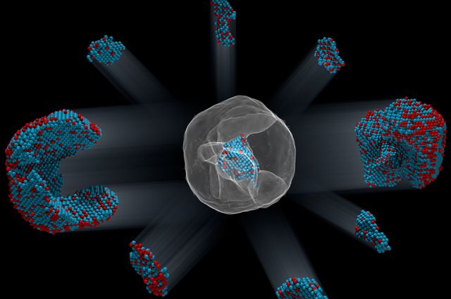
Identification of the precise 3-D coordinates of iron, shown in red, and platinum atoms in an iron-platinum nanoparticle.. Courtesy of Colin Ophus and Florian Nickel/Berkeley Lab
The image of the iron-platinum nanoparticle (referenced in the headline) reminds of foetal ultrasound images. A Feb. 1, 2017 news item on ScienceDaily tells us more,
In the world of the very tiny, perfection is rare: virtually all materials have defects on the atomic level. These imperfections — missing atoms, atoms of one type swapped for another, and misaligned atoms — can uniquely determine a material’s properties and function. Now, UCLA [University of California at Los Angeles] physicists and collaborators have mapped the coordinates of more than 23,000 individual atoms in a tiny iron-platinum nanoparticle to reveal the material’s defects.
The results demonstrate that the positions of tens of thousands of atoms can be precisely identified and then fed into quantum mechanics calculations to correlate imperfections and defects with material properties at the single-atom level.
Jianwei “John” Miao, a UCLA professor of physics and astronomy and a member of UCLA’s California NanoSystems Institute, led the international team in mapping the atomic-level details of the bimetallic nanoparticle, more than a trillion of which could fit within a grain of sand.
“No one has seen this kind of three-dimensional structural complexity with such detail before,” said Miao, who is also a deputy director of the Science and Technology Center on Real-Time Functional Imaging. This new National Science Foundation-funded consortium consists of scientists at UCLA and five other colleges and universities who are using high-resolution imaging to address questions in the physical sciences, life sciences and engineering.
Miao and his team focused on an iron-platinum alloy, a very promising material for next-generation magnetic storage media and permanent magnet applications.
By taking multiple images of the iron-platinum nanoparticle with an advanced electron microscope at Lawrence Berkeley National Laboratory and using powerful reconstruction algorithms developed at UCLA, the researchers determined the precise three-dimensional arrangement of atoms in the nanoparticle.
“For the first time, we can see individual atoms and chemical composition in three dimensions. Everything we look at, it’s new,” Miao said.
The team identified and located more than 6,500 iron and 16,600 platinum atoms and showed how the atoms are arranged in nine grains, each of which contains different ratios of iron and platinum atoms. Miao and his colleagues showed that atoms closer to the interior of the grains are more regularly arranged than those near the surfaces. They also observed that the interfaces between grains, called grain boundaries, are more disordered.
“Understanding the three-dimensional structures of grain boundaries is a major challenge in materials science because they strongly influence the properties of materials,” Miao said. “Now we are able to address this challenge by precisely mapping out the three-dimensional atomic positions at the grain boundaries for the first time.”
The researchers then used the three-dimensional coordinates of the atoms as inputs into quantum mechanics calculations to determine the magnetic properties of the iron-platinum nanoparticle. They observed abrupt changes in magnetic properties at the grain boundaries.
“This work makes significant advances in characterization capabilities and expands our fundamental understanding of structure-property relationships, which is expected to find broad applications in physics, chemistry, materials science, nanoscience and nanotechnology,” Miao said.
In the future, as the researchers continue to determine the three-dimensional atomic coordinates of more materials, they plan to establish an online databank for the physical sciences, analogous to protein databanks for the biological and life sciences. “Researchers can use this databank to study material properties truly on the single-atom level,” Miao said.
Miao and his team also look forward to applying their method called GENFIRE (GENeralized Fourier Iterative Reconstruction) to biological and medical applications. “Our three-dimensional reconstruction algorithm might be useful for imaging like CT scans,” Miao said. Compared with conventional reconstruction methods, GENFIRE requires fewer images to compile an accurate three-dimensional structure.
That means that radiation-sensitive objects can be imaged with lower doses of radiation.
The US Dept. of Energy (DOE) Lawrence Berkeley National Laboratory issued their own Feb. 1, 2017 news release (also on EurekAlert) about the work with a focus on how their equipment made this breakthrough possible (it repeats a little of the info. from the UCLA news release),
Scientists used one of the world’s most powerful electron microscopes to map the precise location and chemical type of 23,000 atoms in an extremely small particle made of iron and platinum.
The 3-D reconstruction reveals the arrangement of atoms in unprecedented detail, enabling the scientists to measure chemical order and disorder in individual grains, which sheds light on the material’s properties at the single-atom level. Insights gained from the particle’s structure could lead to new ways to improve its magnetic performance for use in high-density, next-generation hard drives.
What’s more, the technique used to create the reconstruction, atomic electron tomography (which is like an incredibly high-resolution CT scan), lays the foundation for precisely mapping the atomic composition of other useful nanoparticles. This could reveal how to optimize the particles for more efficient catalysts, stronger materials, and disease-detecting fluorescent tags.
Microscopy data was obtained and analyzed by scientists from the Department of Energy’s Lawrence Berkeley National Laboratory (Berkeley Lab) at the Molecular Foundry, in collaboration with Foundry users from UCLA, Oak Ridge National Laboratory, and the United Kingdom’s University of Birmingham. …
Atoms are the building blocks of matter, and the patterns in which they’re arranged dictate a material’s properties. These patterns can also be exploited to greatly improve a material’s function, which is why scientists are eager to determine the 3-D structure of nanoparticles at the smallest scale possible.
“Our research is a big step in this direction. We can now take a snapshot that shows the positions of all the atoms in a nanoparticle at a specific point in its growth. This will help us learn how nanoparticles grow atom by atom, and it sets the stage for a materials-design approach starting from the smallest building blocks,” says Mary Scott, who conducted the research while she was a Foundry user, and who is now a staff scientist. Scott and fellow Foundry scientists Peter Ercius and Colin Ophus developed the method in close collaboration with Jianwei Miao, a UCLA professor of physics and astronomy.
Their nanoparticle reconstruction builds on an achievement they reported last year in which they measured the coordinates of more than 3,000 atoms in a tungsten needle to a precision of 19 trillionths of a meter (19 picometers), which is many times smaller than a hydrogen atom. Now, they’ve taken the same precision, added the ability to distinguish different elements, and scaled up the reconstruction to include tens of thousands of atoms.
Importantly, their method maps the position of each atom in a single, unique nanoparticle. In contrast, X-ray crystallography and cryo-electron microscopy plot the average position of atoms from many identical samples. These methods make assumptions about the arrangement of atoms, which isn’t a good fit for nanoparticles because no two are alike.
“We need to determine the location and type of each atom to truly understand how a nanoparticle functions at the atomic scale,” says Ercius.
A TEAM approach
The scientists’ latest accomplishment hinged on the use of one of the highest-resolution transmission electron microscopes in the world, called TEAM I. It’s located at the National Center for Electron Microscopy, which is a Molecular Foundry facility. The microscope scans a sample with a focused beam of electrons, and then measures how the electrons interact with the atoms in the sample. It also has a piezo-controlled stage that positions samples with unmatched stability and position-control accuracy.
The researchers began growing an iron-platinum nanoparticle from its constituent elements, and then stopped the particle’s growth before it was fully formed. They placed the “partially baked” particle in the TEAM I stage, obtained a 2-D projection of its atomic structure, rotated it a few degrees, obtained another projection, and so on. Each 2-D projection provides a little more information about the full 3-D structure of the nanoparticle.
They sent the projections to Miao at UCLA, who used a sophisticated computer algorithm to convert the 2-D projections into a 3-D reconstruction of the particle. The individual atomic coordinates and chemical types were then traced from the 3-D density based on the knowledge that iron atoms are lighter than platinum atoms. The resulting atomic structure contains 6,569 iron atoms and 16,627 platinum atoms, with each atom’s coordinates precisely plotted to less than the width of a hydrogen atom.
Translating the data into scientific insights
Interesting features emerged at this extreme scale after Molecular Foundry scientists used code they developed to analyze the atomic structure. For example, the analysis revealed chemical order and disorder in interlocking grains, in which the iron and platinum atoms are arranged in different patterns. This has large implications for how the particle grew and its real-world magnetic properties. The analysis also revealed single-atom defects and the width of disordered boundaries between grains, which was not previously possible in complex 3-D boundaries.
“The important materials science problem we are tackling is how this material transforms from a highly randomized structure, what we call a chemically-disordered structure, into a regular highly-ordered structure with the desired magnetic properties,” says Ophus.
To explore how the various arrangements of atoms affect the nanoparticle’s magnetic properties, scientists from DOE’s Oak Ridge National Laboratory ran computer calculations on the Titan supercomputer at ORNL–using the coordinates and chemical type of each atom–to simulate the nanoparticle’s behavior in a magnetic field. This allowed the scientists to see patterns of atoms that are very magnetic, which is ideal for hard drives. They also saw patterns with poor magnetic properties that could sap a hard drive’s performance.
“This could help scientists learn how to steer the growth of iron-platinum nanoparticles so they develop more highly magnetic patterns of atoms,” says Ercius.
Adds Scott, “More broadly, the imaging technique will shed light on the nucleation and growth of ordered phases within nanoparticles, which isn’t fully theoretically understood but is critically important to several scientific disciplines and technologies.”
The folks at the Berkeley Lab have created a video (notice where the still image from the beginning of this post appears),
The Oak Ridge National Laboratory (ORNL), not wanting to be left out, has been mentioned in a Feb. 3, 2017 news item on ScienceDaily,
… researchers working with magnetic nanoparticles at the University of California, Los Angeles (UCLA), and the US Department of Energy’s (DOE’s) Lawrence Berkeley National Laboratory (Berkeley Lab) approached computational scientists at DOE’s Oak Ridge National Laboratory (ORNL) to help solve a unique problem: to model magnetism at the atomic level using experimental data from a real nanoparticle.
“These types of calculations have been done for ideal particles with ideal crystal structures but not for real particles,” said Markus Eisenbach, a computational scientist at the Oak Ridge Leadership Computing Facility (OLCF), a DOE Office of Science User Facility located at ORNL.
A Feb. 2, 2017 ORNL news release on EurekAlert, which originated the news item, elucidates further on how their team added to the research,
Eisenbach develops quantum mechanical electronic structure simulations that predict magnetic properties in materials. Working with Paul Kent, a computational materials scientist at ORNL’s Center for Nanophase Materials Sciences, the team collaborated with researchers at UCLA and Berkeley Lab’s Molecular Foundry to combine world-class experimental data with world-class computing to do something new–simulate magnetism atom by atom in a real nanoparticle.
Using the new data from the research teams on the West Coast, Eisenbach and Kent were able to precisely model the measured atomic structure, including defects, from a unique iron-platinum (FePt) nanoparticle and simulate its magnetic properties on the 27-petaflop Titan supercomputer at the OLCF.
Electronic structure codes take atomic and chemical structure and solve for the corresponding magnetic properties. However, these structures are typically derived from many 2-D electron microscopy or x-ray crystallography images averaged together, resulting in a representative, but not true, 3-D structure.
“In this case, researchers were able to get the precise 3-D structure for a real particle,” Eisenbach said. “The UCLA group has developed a new experimental technique where they can tell where the atoms are–the coordinates–and the chemical resolution, or what they are — iron or platinum.”
The ORNL news release goes on to describe the work from the perspective of the people who ran the supercompute simulationsr,
A Supercomputing Milestone
Magnetism at the atomic level is driven by quantum mechanics — a fact that has shaken up classical physics calculations and called for increasingly complex, first-principle calculations, or calculations working forward from fundamental physics equations rather than relying on assumptions that reduce computational workload.
For magnetic recording and storage devices, researchers are particularly interested in magnetic anisotropy, or what direction magnetism favors in an atom.
“If the anisotropy is too weak, a bit written to the nanoparticle might flip at room temperature,” Kent said.
To solve for magnetic anisotropy, Eisenbach and Kent used two computational codes to compare and validate results.
To simulate a supercell of about 1,300 atoms from strongly magnetic regions of the 23,000-atom nanoparticle, they used the Linear Scaling Multiple Scattering (LSMS) code, a first-principles density functional theory code developed at ORNL.
“The LSMS code was developed for large magnetic systems and can tackle lots of atoms,” Kent said.
As principal investigator on 2017, 2016, and previous INCITE program awards, Eisenbach has scaled the LSMS code to Titan for a range of magnetic materials projects, and the in-house code has been optimized for Titan’s accelerated architecture, speeding up calculations more than 8 times on the machine’s GPUs. Exceptionally capable of crunching large magnetic systems quickly, the LSMS code received an Association for Computing Machinery Gordon Bell Prize in high-performance computing achievement in 1998 and 2009, and developments continue to enhance the code for new architectures.
Working with Renat Sabirianov at the University of Nebraska at Omaha, the team also ran VASP, a simulation package that is better suited for smaller atom counts, to simulate regions of about 32 atoms.
“With both approaches, we were able to confirm that the local VASP results were consistent with the LSMS results, so we have a high confidence in the simulations,” Eisenbach said.
Computer simulations revealed that grain boundaries have a strong effect on magnetism. “We found that the magnetic anisotropy energy suddenly transitions at the grain boundaries. These magnetic properties are very important,” Miao said.
In the future, researchers hope that advances in computing and simulation will make a full-particle simulation possible — as first-principles calculations are currently too intensive to solve small-scale magnetism for regions larger than a few thousand atoms.
Also, future simulations like these could show how different fabrication processes, such as the temperature at which nanoparticles are formed, influence magnetism and performance.
“There’s a hope going forward that one would be able to use these techniques to look at nanoparticle growth and understand how to optimize growth for performance,” Kent said.
Finally, here’s a link to and a citation for the paper,
Deciphering chemical order/disorder and material properties at the single-atom level by Yongsoo Yang, Chien-Chun Chen, M. C. Scott, Colin Ophus, Rui Xu, Alan Pryor, Li Wu, Fan Sun, Wolfgang Theis, Jihan Zhou, Markus Eisenbach, Paul R. C. Kent, Renat F. Sabirianov, Hao Zeng, Peter Ercius, & Jianwei Miao. Nature 542, 75–79 (02 February 2017) doi:10.1038/nature21042 Published online 01 February 2017
You might want to skip over the reference to snow as it doesn’t have much relevance to this story about ‘melting’, from a Feb. 1, 2017 news item on Nanowerk (Note: A link has been removed),
Snow falls in winter and melts in spring, but what drives the phase change in between?
Although melting is a familiar phenomenon encountered in everyday life, playing a part in many industrial and commercial processes, much remains to be discovered about this transformation at a fundamental level.
In 2015, a team led by the University of Michigan’s Sharon Glotzer used high-performance computing at the Department of Energy’s (DOE’s) Oak Ridge National Laboratory [ORNL] to study melting in two-dimensional (2-D) systems, a problem that could yield insights into surface interactions in materials important to technologies like solar panels, as well as into the mechanism behind three-dimensional melting. The team explored how particle shape affects the physics of a solid-to-fluid melting transition in two dimensions.
Using the Cray XK7 Titan supercomputer at the Oak Ridge Leadership Computing Facility (OLCF), a DOE Office of Science User Facility, the team’s [latest?] work revealed that the shape and symmetry of particles can dramatically affect the melting process (“Shape and symmetry determine two-dimensional melting transitions of hard regular polygons”). This fundamental finding could help guide researchers in search of nanoparticles with desirable properties for energy applications.
There is a video of the ‘melting’ process but I have to confess to finding it a bit enigmatic,
o tackle the problem, Glotzer’s team needed a supercomputer capable of simulating systems of up to 1 million hard polygons, simple particles used as stand-ins for atoms, ranging from triangles to 14-sided shapes. Unlike traditional molecular dynamics simulations that attempt to mimic nature, hard polygon simulations give researchers a pared-down environment in which to evaluate shape-influenced physics.
“Within our simulated 2-D environment, we found that the melting transition follows one of three different scenarios depending on the shape of the systems’ polygons,” University of Michigan research scientist Joshua Anderson said. “Notably, we found that systems made up of hexagons perfectly follow a well-known theory for 2-D melting, something that hasn’t been described until now.”
Shifting Shape Scenarios
In 3-D systems such as a thinning icicle, melting takes the form of a first-order phase transition. This means that collections of molecules within these systems exist in either solid or liquid form with no in-between in the presence of latent heat, the energy that fuels a solid-to-fluid phase change . In 2-D systems, such as thin-film materials used in batteries and other technologies, melting can be more complex, sometimes exhibiting an intermediate phase known as the hexatic phase.
The hexatic phase, a state characterized as a halfway point between an ordered solid and a disordered liquid, was first theorized in the 1970s by researchers John Kosterlitz, David Thouless, Burt Halperin, David Nelson, and Peter Young. The phase is a principle feature of the KTHNY theory, a 2-D melting theory posited by the researchers (and named based on the first letters of their last names). In 2016 Kosterlitz and Thouless were awarded the Nobel Prize in Physics, along with physicist Duncan Haldane, for their contributions to 2-D materials research.
At the molecular level, solid, hexatic, and liquid systems are defined by the arrangement of their atoms. In a crystalline solid, two types of order are present: translational and orientational. Translational order describes the well-defined paths between atoms over distances, like blocks in a carefully constructed Jenga tower. Orientational order describes the relational and clustered order shared between atoms and groups of atoms over distances. Think of that same Jenga tower turned askew after several rounds of play. The general shape of the tower remains, but its order is now fragmented.
The hexatic phase has no translational order but possesses orientational order. (A liquid has neither translational nor orientational order but exhibits short-range order, meaning any atom will have some average number of neighbors nearby but with no predicable order.)
Deducing the presence of a hexatic phase requires a leadership-class computer that can calculate large hard-particle systems. Glotzer’s team gained access to the OLCF’s 27-petaflop Titan through the Innovative and Novel Computational Impact on Theory and Experiment (INCITE) program, running its GPU-accelerated HOOMD-blue code to maximize time on the machine.
On Titan, HOOMD-blue used 64 GPUs for each massively parallel Monte Carlo simulation of up to 1 million particles. Researchers explored 11 different shape systems, applying an external pressure to push the particles together. Each system was simulated at 21 different densities, with the lowest densities representing a fluid state and the highest densities a solid state.
The simulations demonstrated multiple melting scenarios hinging on the polygons’ shape. Systems with polygons of seven sides or more closely followed the melting behavior of hard disks, or circles, exhibiting a continuous phase transition from the solid to the hexatic phase and a first-order phase transition from the hexatic to the liquid phase. A continuous phase transition means a constantly changing area in response to a changing external pressure. A first-order phase transition is characterized by a discontinuity in which the volume jumps across the phase transition in response to the changing external pressure. The team found pentagons and fourfold pentilles, irregular pentagons with two different edge lengths, exhibit a first-order solid-to-liquid phase transition.
The most significant finding, however, emerged from hexagon systems, which perfectly followed the phase transition described by the KTHNY theory. In this scenario, the particles’ shift from solid to hexatic and hexatic to fluid in a perfect continuous phase transition pattern.
“It was actually sort of surprising that no one else has found that until now,” Anderson said, “because it seems natural that the hexagon, with its six sides, and the honeycomb-like hexagonal arrangement would be a perfect match for this theory” in which the hexatic phase generally contains sixfold orientational order.
Glotzer’s team, which recently received a 2017 INCITE allocation, is now applying its leadership-class computing prowess to tackle phase transitions in 3-D. The team is focusing on how fluid particles crystallize into complex colloids—mixtures in which particles are suspended throughout another substance. Common examples of colloids include milk, paper, fog, and stained glass.
“We’re planning on using Titan to study how complexity can arise from these simple interactions, and to do that we’re actually going to look at how the crystals grow and study the kinetics of how that happens,” said Anderson.
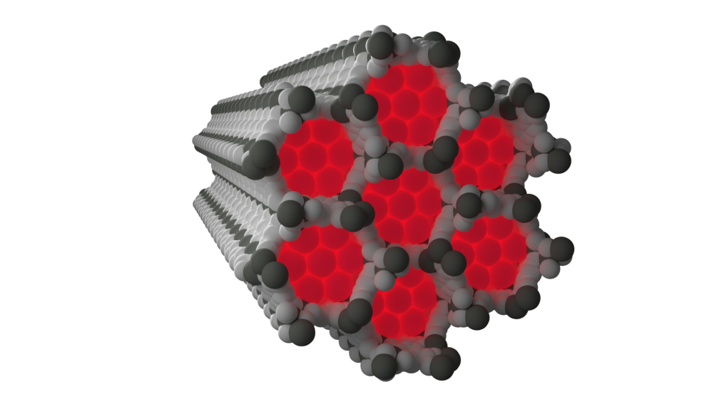
Layers of graphene separated by nanotube pillars of boron nitride may be a suitable material to store hydrogen fuel in cars, according to Rice University scientists.
The Department of Energy has set benchmarks for storage materials that would make hydrogen a practical fuel for light-duty vehicles. The Rice lab of materials scientist Rouzbeh Shahsavari determined in a new computational study that pillared boron nitride and graphene could be a candidate.
Shahsavari’s lab had already determined through computer models how tough and resilient pillared graphene structures would be, and later worked boron nitride nanotubes into the mix to model a unique three-dimensional architecture. (Samples of boron nitride nanotubes seamlessly bonded to graphene have been made.)
Just as pillars in a building make space between floors for people, pillars in boron nitride graphene make space for hydrogen atoms. The challenge is to make them enter and stay in sufficient numbers and exit upon demand.
In their latest molecular dynamics simulations, the researchers found that either pillared graphene or pillared boron nitride graphene would offer abundant surface area (about 2,547 square meters per gram) with good recyclable properties under ambient conditions. Their models showed adding oxygen or lithium to the materials would make them even better at binding hydrogen.
They focused the simulations on four variants: pillared structures of boron nitride or pillared boron nitride graphene doped with either oxygen or lithium. At room temperature and in ambient pressure, oxygen-doped boron nitride graphene proved the best, holding 11.6 percent of its weight in hydrogen (its gravimetric capacity) and about 60 grams per liter (its volumetric capacity); it easily beat competing technologies like porous boron nitride, metal oxide frameworks and carbon nanotubes.
At a chilly -321 degrees Fahrenheit, the material held 14.77 percent of its weight in hydrogen.
The Department of Energy’s current target for economic storage media is the ability to store more than 5.5 percent of its weight and 40 grams per liter in hydrogen under moderate conditions. The ultimate targets are 7.5 weight percent and 70 grams per liter.
Shahsavari said hydrogen atoms adsorbed to the undoped pillared boron nitride graphene, thanks to weak van der Waals forces. When the material was doped with oxygen, the atoms bonded strongly with the hybrid and created a better surface for incoming hydrogen, which Shahsavari said would likely be delivered under pressure and would exit when pressure is released.
“Adding oxygen to the substrate gives us good bonding because of the nature of the charges and their interactions,” he said. “Oxygen and hydrogen are known to have good chemical affinity.”
He said the polarized nature of the boron nitride where it bonds with the graphene and the electron mobility of the graphene itself make the material highly tunable for applications.
“What we’re looking for is the sweet spot,” Shahsavari said, describing the ideal conditions as a balance between the material’s surface area and weight, as well as the operating temperatures and pressures. “This is only practical through computational modeling, because we can test a lot of variations very quickly. It would take experimentalists months to do what takes us only days.”
He said the structures should be robust enough to easily surpass the Department of Energy requirement that a hydrogen fuel tank be able to withstand 1,500 charge-discharge cycles.
Shayeganfar [Farzaneh Shayeganfar], a former visiting scholar at Rice, is an instructor at Shahid Rajaee Teacher Training University in Tehran, Iran.
Caption: Simulations by Rice University scientists show that pillared graphene boron nitride may be a suitable storage medium for hydrogen-powered vehicles. Above, the pink (boron) and blue (nitrogen) pillars serve as spacers for carbon graphene sheets (gray). The researchers showed the material worked best when doped with oxygen atoms (red), which enhanced its ability to adsorb and desorb hydrogen (white). Credit: Lei Tao/Rice University
The University of California at Davis (UC Davis) and the University of Washington (state) collaborated in research into fundamental questions on how aquatic animals grow. From an Oct. 24, 2016 news item on ScienceDaily,
For the first time scientists can see how the shells of tiny marine organisms grow atom-by-atom, a new study reports. The advance provides new insights into the mechanisms of biomineralization and will improve our understanding of environmental change in Earth’s past.
Led by researchers from the University of California, Davis and the University of Washington, with key support from the U.S. Department of Energy’s Pacific Northwest National Laboratory, the team examined an organic-mineral interface where the first calcium carbonate crystals start to appear in the shells of foraminifera, a type of plankton.
“We’ve gotten the first glimpse of the biological event horizon,” said Howard Spero, a study co-author and UC Davis geochemistry professor. …
Foraminifera’s Final Frontier
The researchers zoomed into shells at the atomic level to better understand how growth processes may influence the levels of trace impurities in shells. The team looked at a key stage — the interaction between the biological ‘template’ and the initiation of shell growth. The scientists produced an atom-scale map of the chemistry at this crucial interface in the foraminifera Orbulina universa. This is the first-ever measurement of the chemistry of a calcium carbonate biomineralization template, Spero said.
Among the new findings are elevated levels of sodium and magnesium in the organic layer. This is surprising because the two elements are not considered important architects in building shells, said lead study author Oscar Branson, a former postdoctoral researcher at UC Davis who is now at the Australian National University in Canberra. Also, the greater concentrations of magnesium and sodium in the organic template may need to be considered when investigating past climate with foraminifera shells.
Calibrating Earth’s Climate
Most of what we know about past climate (beyond ice core records) comes from chemical analyses of shells made by the tiny, one-celled creatures called foraminifera, or “forams.” When forams die, their shells sink and are preserved in seafloor mud. The chemistry preserved in ancient shells chronicles climate change on Earth, an archive that stretches back nearly 200 million years.
The calcium carbonate shells incorporate elements from seawater — such as calcium, magnesium and sodium — as the shells grow. The amount of trace impurities in a shell depends on both the surrounding environmental conditions and how the shells are made. For example, the more magnesium a shell has, the warmer the ocean was where that shell grew.
“Finding out how much magnesium there is in a shell can allow us to find out the temperature of seawater going back up to 150 million years,” Branson said.
But magnesium levels also vary within a shell, because of nanometer-scale growth bands. Each band is one day’s growth (similar to the seasonal variations in tree rings). Branson said considerable gaps persist in understanding what exactly causes the daily bands in the shells.
“We know that shell formation processes are important for shell chemistry, but we don’t know much about these processes or how they might have changed through time,” he said. “This adds considerable uncertainty to climate reconstructions.”
Atomic Maps
The researchers used two cutting-edge techniques: Time-of-Flight Secondary Ionization Mass Spectrometry (ToF-SIMS) and Laser-Assisted Atom Probe Tomography (APT). ToF-SIMS is a two-dimensional chemical mapping technique which shows the elemental composition of the surface of a polished sample. The technique was developed for the elemental analysis of complex polymer materials, and is just starting to be applied to natural samples like shells.
APT is an atomic-scale three-dimensional mapping technique, developed for looking at internal structures in advanced alloys, silicon chips and superconductors. The APT imaging was performed at the Environmental Molecular Sciences Laboratory, a U.S. Department of Energy Office of Science User Facility at the Pacific Northwest National Laboratory.
This foraminifera is just starting to form its adult spherical shell. The calcium carbonate spherical shell first forms on a thin organic template, shown here in white, around the dark juvenile skeleton. Calcium carbonate spines then extend from the juvenile skeleton through the new sphere and outward. The bright flecks are algae that the foraminifera “farm” for sustenance.Howard Spero/University of California, Davis
Unseen out in the ocean, countless single-celled organisms grow protective shells to keep them safe as they drift along, living off other tiny marine plants and animals. Taken together, the shells are so plentiful that when they sink they provide one of the best records for the history of ocean chemistry.
Oceanographers at the University of Washington and the University of California, Davis, have used modern tools to provide an atomic-scale look at how that shell first forms. Results could help answer fundamental questions about how these creatures grow under different ocean conditions, in the past and in the future. …
“There’s this debate among scientists about whether shelled organisms are slaves to the chemistry of the ocean, or whether they have the physiological capacity to adapt to changing environmental conditions,” said senior author Alex Gagnon, a UW assistant professor of oceanography.
The new work shows, he said, that they do exert some biologically-based control over shell formation.
“I think it’s just incredible that we were able to peer into the intricate details of those first moments that set how a seashell forms,” Gagnon said. “And that’s what sets how much of the rest of the skeleton will grow.”
The results could eventually help understand how organisms at the base of the marine food chain will respond to more acidic waters. And while the study looked at one organism, Orbulina universa, which is important for understanding past climate, the same method could be used for other plankton, corals and shellfish.
The study used tools developed for materials science and semiconductor research to view the shell formation in the most detail yet to see how the organisms turn seawater into solid mineral.
“We’re interested more broadly in the question ‘How do organisms make shells?'” said first author Oscar Branson, a former postdoctoral researcher at the University of California, Davis who is now at Australian National University in Canberra. “We’ve focused on a key stage in mineral formation — the interaction between biological template materials and the initiation of shell growth by an organism.”
These tiny single-celled animals, called foraminifera, can’t reproduce anywhere but in their natural surroundings, which prevents breeding them in captivity. The researchers caught juvenile foraminifera by diving in deep water off Southern California. Then they then raised them in the lab, using tiny pipettes to feed them brine shrimp during their weeklong lives.
Marine shells are made from calcium carbonate, drawing the calcium and carbon from surrounding seawater. But the animal first grows a soft template for the mineral to grow over. Because this template is trapped within the growing skeleton, it acts as a snapshot of the chemical conditions during the first part of skeletal growth.
To see this chemical picture, the authors analyzed tiny sections of foraminifera template with a technique called atom probe tomography at the Pacific Northwest National Laboratory. This tool creates an atom-by-atom picture of the organic template, which was located using a chemical tag.
Results show that the template contains more magnesium and sodium atoms than expected, and that this could influence how the mineral in the shell begins to grow around it.
“One of the key stages in growing a skeleton is when you make that first bit, when you build that first bit of structure. Anything that changes that process is a key control point,” Gagnon said.
The clumping suggests that magnesium and sodium play a role in the first stages of shell growth. If their availability changes for any reason, that could influence how the shell grows beyond what simple chemistry would predict.
“We can say who the players are — further experiments will have to tell us exactly how important each of them is,” Gagnon said.
Follow-up work will try to grow the shells and create models of their formation to see how the template affects growth under different conditions, such as more acidic water.
“Translating that into, ‘Can these forams survive ocean acidification?’ is still many steps down the line,” Gagnon cautioned. “But you can’t do that until you have a picture of what that surface actually looks like.”
The researchers also hope that by better understanding the exact mechanism of shell growth they could tease apart different aspects of seafloor remains so the shells can be used to reconstruct more than just the ocean’s past temperature. In the study, they showed that the template was responsible for causing fine lines in the shells — one example of the rich chemical information encoded in fossil shells.
“There are ways that you could separate the effects of temperature from other things and learn much more about the past ocean,” Gagnon said.
Here’s a link to and a citation for the paper,
Nanometer-Scale Chemistry of a Calcite Biomineralization Template: Implications for Skeletal Composition and Nucleation, Proceedings of the National Academy of Sciences, www.pnas.org/cgi/doi/10.1073/pnas.1522864113
An Oct. 12, 2016 news item on ScienceDaily makes an exciting announcement, if carbon-dixoide-conversion-to-fuel is one of your pet topics,
In a new twist to waste-to-fuel technology, scientists at the Department of Energy’s Oak Ridge National Laboratory [ORNL] have developed an electrochemical process that uses tiny spikes of carbon and copper to turn carbon dioxide, a greenhouse gas, into ethanol. Their finding, which involves nanofabrication and catalysis science, was serendipitous.
“We discovered somewhat by accident that this material worked,” said ORNL’s Adam Rondinone, lead author of the team’s study published in ChemistrySelect. “We were trying to study the first step of a proposed reaction when we realized that the catalyst was doing the entire reaction on its own.”
The team used a catalyst made of carbon, copper and nitrogen and applied voltage to trigger a complicated chemical reaction that essentially reverses the combustion process. With the help of the nanotechnology-based catalyst which contains multiple reaction sites, the solution of carbon dioxide dissolved in water turned into ethanol with a yield of 63 percent. Typically, this type of electrochemical reaction results in a mix of several different products in small amounts.
“We’re taking carbon dioxide, a waste product of combustion, and we’re pushing that combustion reaction backwards with very high selectivity to a useful fuel,” Rondinone said. “Ethanol was a surprise — it’s extremely difficult to go straight from carbon dioxide to ethanol with a single catalyst.”
The catalyst’s novelty lies in its nanoscale structure, consisting of copper nanoparticles embedded in carbon spikes. This nano-texturing approach avoids the use of expensive or rare metals such as platinum that limit the economic viability of many catalysts.
“By using common materials, but arranging them with nanotechnology, we figured out how to limit the side reactions and end up with the one thing that we want,” Rondinone said.
The researchers’ initial analysis suggests that the spiky textured surface of the catalysts provides ample reactive sites to facilitate the carbon dioxide-to-ethanol conversion.
“They are like 50-nanometer lightning rods that concentrate electrochemical reactivity at the tip of the spike,” Rondinone said.
Given the technique’s reliance on low-cost materials and an ability to operate at room temperature in water, the researchers believe the approach could be scaled up for industrially relevant applications. For instance, the process could be used to store excess electricity generated from variable power sources such as wind and solar.
“A process like this would allow you to consume extra electricity when it’s available to make and store as ethanol,” Rondinone said. “This could help to balance a grid supplied by intermittent renewable sources.”
The researchers plan to refine their approach to improve the overall production rate and further study the catalyst’s properties and behavior.
A Sept. 8, 2016 news item on Nanowerk describes research into producing remarkably stable gold nanoparticles with catalytic capabilities (Note: A link has been removed),
An ultra-high-vacuum chamber with temperatures approaching absolute zero—the coldest anything can get—may be the last place you would expect to find gold. But a group of researchers from Stony Brook University (SBU) in collaboration with scientists at the Air Force Research Lab (AFRL) and the U.S. Department of Energy’s (DOE) Brookhaven National Laboratory have just demonstrated that such a desolate place is ideal for producing catalytically active gold nanoparticles.
A paper describing the first catalyst ever produced using their new method, called Helium Nanodroplet Deposition (HND), was recently published in the Journal of Physical Chemistry Letters (“Development of a New Generation of Stable, Tunable, and Catalytically Active Nanoparticles Produced by the Helium Nanodroplet Deposition Method”).
As lead researcher Alexander Orlov of SBU explains, HND works by boiling gold atoms in a vacuum to produce a vapor. The vaporized gold is then “picked up” by an extremely cold jet stream of liquid helium droplets that act to literally strike gold clusters against a solid collector downstream. Upon striking the collector, the liquid helium droplets instantly evaporate releasing helium gas and leaving behind unprecedentedly pure and stable gold nanoparticles.
“This new method to produce active nanoparticles offers unique opportunities to create materials with unprecedented properties to solve energy and environmental problems,” Orlov said. “Our Brookhaven and AFRL collaborators made it possible for our students to access the most unique facilities in the world, which made all the difference in our research.”
Qiyuan Wu, a graduate student working in Orlov’s laboratory and first author on the paper, performed much of the work to develop the method. Michael Lindsay and Claron Ridge of AFRL provided state-of-the-art facilities at Eglin Air Force Base, one of only a few places in the world with the capabilities required to generate the gold nanoparticles using the new technique. And a team at the Center for Functional Nanomaterials (CFN), a DOE Office of Science User Facility at Brookhaven Lab, used advanced imaging and characterization tools to study the nanoparticles’ catalytic activity.
Specifically, Brookhaven scientists Eric Stach and Dmitri Zakharov of the CFN and Shen Zhao, then a postdoctoral fellow working under Stach, developed a method to deposit the gold nanoparticles onto a “catalyst support” structure they use for characterizing the stability of other nanomaterials. They then studied the characteristics of the nanoparticles, including their stability under reaction conditions, using the Titan Environmental Transmission Electron Microscope at the CFN. Further characterization by Zhao and CFN staff member Dong Su using aberration-corrected Scanning Transmission Electron Microscopy allowed the SBU researchers to understand how the droplets form.
“This was part of a User project, that morphed into a collaboration,” said Stach, who leads the electron microscopy group at CFN. “It was a very nice study”—and an example of how the Office of Science User Facilities offer not just unique scientific equipment but also scientific expertise that can be essential to the success of a research project.
Nanoparticles are of high research interest due to their improved properties compared to bulk materials. They have revolutionized technologies aimed at improving sustainability such as fuel cells, photocatalysts, and solar panels. The gold nanoparticle catalysts produced in this study are capable of converting poisonous carbon monoxide gas into carbon dioxide gas, an essential reaction that occurs in the catalytic converters of cars to reduce pollution and lower impacts on the environment.
According to Orlov, the HND method is not limited to the production of gold nanoparticles, but can be applied to nearly all metals and can even produce challenging multi-metallic nanoparticles. The technique’s versatility and ability to produce clean and well-defined samples make it a powerful tool for the discovery of new catalysts and studying factors that affect catalyst performance.
The collaboration is currently researching how the parameters of HND can be adjusted to control catalyst performance.
It’s been a while since I’ve had a story about electrochromic windows and I’ve begun to despair that they will ever reach the marketplace. Happily, the Massachusetts Institute of Technology (MIT) has supplied a ray of light (intentional wordplay). An Aug. 11, 2016 news item on Nanowerk makes the announcement,
A team of researchers at MIT has developed a new way of making windows that can switch from transparent to opaque, potentially saving energy by blocking sunlight on hot days and thus reducing air-conditioning costs. While other systems for causing glass to darken do exist, the new method offers significant advantages by combining rapid response times and low power needs.
Once the glass is switched from clear to dark, or vice versa, the new system requires little to no power to maintain its new state; unlike other materials, it only needs electricity when it’s time to switch back again.
The new discovery uses electrochromic materials, which change their color and transparency in response to an applied voltage, Dinca [MIT professor of chemistry Mircea Dinca] explains. These are quite different from photochromic materials, such as those found in some eyeglasses that become darker when the light gets brighter. Such materials tend to have much slower response times and to undergo a smaller change in their levels of opacity.
Existing electrochromic materials suffer from similar limitations and have found only niche applications. For example, Boeing 787 aircraft have electrochromic windows that get darker to prevent bright sunlight from glaring through the cabin. The windows can be darkened by turning on the voltage, Dinca says, but “when you flip the switch, it actually takes a few minutes for the window to turn dark. Obviously, you want that to be faster.”
The reason for that slowness is that the changes within the material rely on a movement of electrons — an electric current — that gives the whole window a negative charge. Positive ions then move through the material to restore the electrical balance, creating the color-changing effect. But while electrons flow rapidly through materials, ions move much more slowly, limiting the overall reaction speed.
The MIT team overcame that by using sponge-like materials called metal-organic frameworks (MOFs), which can conduct both electrons and ions at very high speeds. Such materials have been used for about 20 years for their ability to store gases within their structure, but the MIT team was the first to harness them for their electrical and optical properties.
The other problem with existing versions of self-shading materials, Dinca says, is that “it’s hard to get a material that changes from completely transparent to, let’s say, completely black.” Even the windows in the 787 can only change to a dark shade of green, rather than becoming opaque.
In previous research on MOFs, Dinca and his students had made material that could turn from clear to shades of blue or green, but in this newly reported work they have achieved the long-sought goal of producing a coating that can go all the way from perfectly clear to nearly black (achieved by blending two complementary colors, green and red). The new material is made by combining two chemical compounds, an organic material and a metal salt. Once mixed, these self-assemble into a thin film of the switchable material.
“It’s this combination of these two, of a relatively fast switching time and a nearly black color, that has really got people excited,” Dinca says.
The new windows have the potential, he says, to do much more than just preventing glare. “These could lead to pretty significant energy savings,” he says, by drastically reducing the need for air conditioning in buildings with many windows in hot climates. “You could just flip a switch when the sun shines through the window, and turn it dark,” or even automatically make that whole side of the building go dark all at once, he says.
While the properties of the material have now been demonstrated in a laboratory setting, the team’s next step is to make a small-scale device for further testing: a 1-inch-square sample, to demonstrate the principle in action for potential investors in the technology, and to help determine what the manufacturing costs for such windows would be.
Further testing is also needed, Dinca says, to demonstrate what they have determined from preliminary testing: that once the switch is flipped and the material changes color, it requires no further power to maintain its new state. No extra power is needed until the switch is flipped to turn the material back to its former state, whether clear or opaque. Many existing electrochromic materials, by contrast, require a continuous voltage input.
In addition to smart windows, Dinca says, the material could also be used for some kinds of low-power displays, similar to displays like electronic ink (used in devices such as the Kindle and based on MIT-developed technology) but based on a completely different approach.
Not surprisingly perhaps, the research was partly funded by an organization in a region where such light-blocking windows would be particularly useful: The Masdar Institute, based in the United Arab Emirates, through a cooperative agreement with MIT. The research also received support from the U.S. Department of Energy, through the Center for Excitonics, an Energy Frontier Center.
Neon observed experimentally within the pores of NiMOF-74 at 100 K and 100 bar of neon gas pressure Courtesy: Cambridge Crystallographic Data Centre (CCDC)
An Aug. 10, 2016 news item on Nanowerk announces the breakthrough (Note: A link has been removed),
In a new study, researchers from the Cambridge Crystallographic Data Centre (CCDC) and the U.S. Department of Energy’s (DOE’s) Argonne National Laboratory have teamed up to capture neon within a porous crystalline framework. Neon is well known for being the most unreactive element and is a key component in semiconductor manufacturing, but neon has never been studied within an organic or metal-organic framework until now.
The results (Chemical Communications, “Capturing neon – the first experimental structure of neon trapped within a metal–organic environment”), which include the critical studies carried out at the Advanced Photon Source (APS), a DOE Office of Science user facility at Argonne, also point the way towards a more economical and greener industrial process for neon production.
Neon is an element that is well-known to the general public due to its iconic use in neon signs, especially in city centres in the United States from the 1920s to the 1960s. In recent years, the industrial use of neon has become dominated by use in excimer lasers to produce semiconductors. Despite being the fifth most abundant element in the atmosphere, the cost of pure neon gas has risen significantly over the years, increasing the demand for better ways to separate and isolate the gas.
During 2015, CCDC scientists presented a talk at the annual American Crystallographic Association (ACA) meeting on the array of elements that have been studied within an organic or metal-organic environment, challenging the crystallographic community to find the next and possibly last element to be added to the Cambridge Structural Database (CSD). A chance encounter at that meeting with Andrey Yakovenko, a beamline scientist at the Advanced Photon Source, resulted in a collaborative project to capture neon – the 95th element to be observed in the CSD.
Neon’s low reactivity, along with the weak scattering of X-rays due to its relatively low number of electrons, means that conclusive experimental observation of neon captured within a crystalline framework is very challenging. In situ high pressure gas flow experiments performed at X-Ray Science Division beamline 17-BM at the APS using the X-ray powder diffraction technique at low temperatures managed to elucidate the structure of two different metal-organic frameworks with neon gas captured within the materials.
“This is a really exciting moment representing the latest new element to be added to the CSD and quite possibly the last given the experimental and safety challenges associated with the other elements yet to be studied” said Peter Wood, Senior Research Scientist at CCDC and lead author on the paper published in Chemical Communications. “More importantly, the structures reported here show the first observation of a genuine interaction between neon and a transition metal, suggesting the potential for future design of selective neon capture frameworks”.
The structure of neon captured within the framework known as NiMOF-74, a porous framework built from nickel metal centres and organic linkers, shows clear nickel to neon interactions forming at low temperatures significantly shorter than would be expected from a typical weak contact.
Andrey Yakovenko said “These fascinating results show the great capabilities of the scientific program at 17-BM and the Advanced Photon Source. Previously we have been doing experiments at our beamline using other much heavier, and therefore easily detectable, noble gases such as xenon and krypton. However, after meeting co-authors Pete, Colin, Amy and Suzanna at the ACA meeting, we decided to perform these much more complicated experiments using the very light and inert gas – neon. In fact, only by using a combination of in situ X-ray powder diffraction measurements, low temperature and high pressure have we been able to conclusively identify the neon atom positions beyond reasonable doubt”.
Summarising the findings, Chris Cahill, Past President of the ACA and Professor of Chemistry, George Washington University said “This is a really elegant piece of in situ crystallography research and it is particularly pleasing to see the collaboration coming about through discussions at an annual ACA meeting”.
Self-assembly in this context references the notion of ‘bottom-up engineering’, that is, following nature’s engineering process where elements assemble themselves into a plant, animal, or something else. Humans have for centuries used an approach known as ‘top-down engineering’ where we take materials and reform them, e.g., trees into paper or houses.
Theoretically, bottom-up engineering (self-assembly) is more efficient than top-down engineering but we have yet to become as skilled as Nature at the process.
Scientists at the US Brookhaven National Laboratory believe they have taken a step in the right direction with regard to self-assembly. From an Aug. 8, 2016 Brookhaven National Laboratory news release (also on EurekAlert) by Justin Eure describes the research (Note: A link has been removed),
To continue advancing, next-generation electronic devices must fully exploit the nanoscale, where materials span just billionths of a meter. But balancing complexity, precision, and manufacturing scalability on such fantastically small scales is inevitably difficult. Fortunately, some nanomaterials can be coaxed into snapping themselves into desired formations-a process called self-assembly.
Scientists at the U.S. Department of Energy’s (DOE) Brookhaven National Laboratory have just developed a way to direct the self-assembly of multiple molecular patterns within a single material, producing new nanoscale architectures. The results were published in the journal Nature Communications.
“This is a significant conceptual leap in self-assembly,” said Brookhaven Lab physicist Aaron Stein, lead author on the study. “In the past, we were limited to a single emergent pattern, but this technique breaks that barrier with relative ease. This is significant for basic research, certainly, but it could also change the way we design and manufacture electronics.”
Microchips, for example, use meticulously patterned templates to produce the nanoscale structures that process and store information. Through self-assembly, however, these structures can spontaneously form without that exhaustive preliminary patterning. And now, self-assembly can generate multiple distinct patterns-greatly increasing the complexity of nanostructures that can be formed in a single step.
“This technique fits quite easily into existing microchip fabrication workflows,” said study coauthor Kevin Yager, also a Brookhaven physicist. “It’s exciting to make a fundamental discovery that could one day find its way into our computers.”
The experimental work was conducted entirely at Brookhaven Lab’s Center for Functional Nanomaterials (CFN), a DOE Office of Science User Facility, leveraging in-house expertise and instrumentation.
Cooking up organized complexity
The collaboration used block copolymers-chains of two distinct molecules linked together-because of their intrinsic ability to self-assemble.
“As powerful as self-assembly is, we suspected that guiding the process would enhance it to create truly ‘responsive’ self-assembly,” said study coauthor Greg Doerk of Brookhaven. “That’s exactly where we pushed it.”
To guide self-assembly, scientists create precise but simple substrate templates. Using a method called electron beam lithography-Stein’s specialty-they etch patterns thousands of times thinner than a human hair on the template surface. They then add a solution containing a set of block copolymers onto the template, spin the substrate to create a thin coating, and “bake” it all in an oven to kick the molecules into formation. Thermal energy drives interaction between the block copolymers and the template, setting the final configuration-in this instance, parallel lines or dots in a grid.
“In conventional self-assembly, the final nanostructures follow the template’s guiding lines, but are of a single pattern type,” Stein said. “But that all just changed.”
Lines and dots, living together
The collaboration had previously discovered that mixing together different block copolymers allowed multiple, co-existing line and dot nanostructures to form.
“We had discovered an exciting phenomenon, but couldn’t select which morphology would emerge,” Yager said. But then the team found that tweaking the substrate changed the structures that emerged. By simply adjusting the spacing and thickness of the lithographic line patterns-easy to fabricate using modern tools-the self-assembling blocks can be locally converted into ultra-thin lines, or high-density arrays of nano-dots.
“We realized that combining our self-assembling materials with nanofabricated guides gave us that elusive control. And, of course, these new geometries are achieved on an incredibly small scale,” said Yager.
“In essence,” said Stein, “we’ve created ‘smart’ templates for nanomaterial self-assembly. How far we can push the technique remains to be seen, but it opens some very promising pathways.”
Gwen Wright, another CFN coauthor, added, “Many nano-fabrication labs should be able to do this tomorrow with their in-house tools-the trick was discovering it was even possible.”
The scientists plan to increase the sophistication of the process, using more complex materials in order to move toward more device-like architectures.
“The ongoing and open collaboration within the CFN made this possible,” said Charles Black, director of the CFN. “We had experts in self-assembly, electron beam lithography, and even electron microscopy to characterize the materials, all under one roof, all pushing the limits of nanoscience.”