Tag Archives: Eindhoven University of Technology

Organic neuromorphic electronics

A December 13, 2021 news item on ScienceDaily describes some research from Germany’s Max Planck Institute for Polymer Research,

The human brain works differently from a computer – while the brain works with biological cells and electrical impulses, a computer uses silicon-based transistors. Scientists have equipped a toy robot with a smart and adaptive electrical circuit made of soft organic materials, similarly to the biological matter. With this bio-inspired approach, they were able to teach the robot to navigate independently through a maze using visual signs for guidance.

A December 13, 2021 Max Planck Institute for Polymer Research press release (also on EurekAlert), which originated the news item, fills in a few details,

The processor is the brain of a computer – an often-quoted phrase. But processors work fundamentally differently than the human brain. Transistors perform logic operations by means of electronic signals. In contrast, the brain works with nerve cells, so-called neurons, which are connected via biological conductive paths, so-called synapses. At a higher level, this signaling is used by the brain to control the body and perceive the surrounding environment. The reaction of the body/brain system when certain stimuli are perceived – for example, via the eyes, ears or sense of touch – is triggered through a learning process. For example, children learn not to reach twice for a hot stove: one input stimulus leads to a learning process with a clear behavioral outcome.

Scientists working with Paschalis Gkoupidenis, group leader in Paul Blom’s department at the Max Planck Institute for Polymer Research, have now applied this basic principle of learning through experience in a simplified form and steered a robot through a maze using a so-called organic neuromorphic circuit. The work was an extensive collaboration between the Universities of Eindhoven [Eindhoven University of Technology; Netherlands], Stanford [University; California, US], Brescia [University; Italy], Oxford [UK] and KAUST [King Abdullah University of Science and Technology, Saudi Arabia].

“We wanted to use this simple setup to show how powerful such ‘organic neuromorphic devices’ can be in real-world conditions,” says Imke Krauhausen, a doctoral student in Gkoupidenis’ group and at TU Eindhoven (van de Burgt group), and first author of the scientific paper.

To achieve the navigation of the robot inside the maze, the researchers fed the smart adaptive circuit with sensory signals coming from the environment. The path of maze towards the exit is indicated visually at each maze intersects. Initially, the robot often misinterprets the visual signs, thus it makes the wrong “turning” decisions at the maze intersects and loses the way out. When the robot takes these decisions and follows wrong dead-end paths, it is being discouraged to take these wrong decisions by receiving corrective stimuli. The corrective stimuli, for example when the robot hits a wall, are directly applied at the organic circuit via electrical signals induced by a touch sensor attached to the robot. With each subsequent execution of the experiment, the robot gradually learns to make the right “turning” decisions at the intersects, i. e. to avoid receiving corrective stimuli, and after a few trials it finds the way out of the maze. This learning process happens exclusively on the organic adaptive circuit. 

“We were really glad to see that the robot can pass through the maze after some runs by learning on a simple organic circuit. We have shown here a first, very simple setup. In the distant future, however, we hope that organic neuromorphic devices could also be used for local and distributed computing/learning. This will open up entirely new possibilities for applications in real-world robotics, human-machine interfaces and point-of-care diagnostics. Novel platforms for rapid prototyping and education, at the intersection of materials science and robotics, are also expected to emerge.” Gkoupidenis says.

Here’s a link to and a citation for the paper,

Organic neuromorphic electronics for sensorimotor integration and learning in robotics by Imke Krauhausen, Dimitrios A. Koutsouras, Armantas Melianas, Scott T. Keene, Katharina Lieberth, Hadrien Ledanseur, Rajendar Sheelamanthula, Alexander Giovannitti, Fabrizio Torricelli, Iain Mcculloch, Paul W. M. Blom, Alberto Salleo, Yoeri van de Burgt and Paschalis Gkoupidenis. Science Advances • 10 Dec 2021 • Vol 7, Issue 50 • DOI: 10.1126/sciadv.abl5068

This paper is open access.

A biohybrid artificial synapse that can communicate with living cells

As I noted in my June 16, 2020 posting, we may have more than one kind of artificial brain in our future. This latest work features a biohybrid. From a June 15, 2020 news item on ScienceDaily,

In 2017, Stanford University researchers presented a new device that mimics the brain’s efficient and low-energy neural learning process [see my March 8, 2017 posting for more]. It was an artificial version of a synapse — the gap across which neurotransmitters travel to communicate between neurons — made from organic materials. In 2019, the researchers assembled nine of their artificial synapses together in an array, showing that they could be simultaneously programmed to mimic the parallel operation of the brain [see my Sept. 17, 2019 posting].

Now, in a paper published June 15 [2020] in Nature Materials, they have tested the first biohybrid version of their artificial synapse and demonstrated that it can communicate with living cells. Future technologies stemming from this device could function by responding directly to chemical signals from the brain. The research was conducted in collaboration with researchers at Istituto Italiano di Tecnologia (Italian Institute of Technology — IIT) in Italy and at Eindhoven University of Technology (Netherlands).

“This paper really highlights the unique strength of the materials that we use in being able to interact with living matter,” said Alberto Salleo, professor of materials science and engineering at Stanford and co-senior author of the paper. “The cells are happy sitting on the soft polymer. But the compatibility goes deeper: These materials work with the same molecules neurons use naturally.”

While other brain-integrated devices require an electrical signal to detect and process the brain’s messages, the communications between this device and living cells occur through electrochemistry — as though the material were just another neuron receiving messages from its neighbor.

A June 15, 2020 Stanford University news release (also on EurekAlert) by Taylor Kubota, which originated the news item, delves further into this recent work,

How neurons learn

The biohybrid artificial synapse consists of two soft polymer electrodes, separated by a trench filled with electrolyte solution – which plays the part of the synaptic cleft that separates communicating neurons in the brain. When living cells are placed on top of one electrode, neurotransmitters that those cells release can react with that electrode to produce ions. Those ions travel across the trench to the second electrode and modulate the conductive state of this electrode. Some of that change is preserved, simulating the learning process occurring in nature.

“In a biological synapse, essentially everything is controlled by chemical interactions at the synaptic junction. Whenever the cells communicate with one another, they’re using chemistry,” said Scott Keene, a graduate student at Stanford and co-lead author of the paper. “Being able to interact with the brain’s natural chemistry gives the device added utility.”

This process mimics the same kind of learning seen in biological synapses, which is highly efficient in terms of energy because computing and memory storage happen in one action. In more traditional computer systems, the data is processed first and then later moved to storage.

To test their device, the researchers used rat neuroendocrine cells that release the neurotransmitter dopamine. Before they ran their experiment, they were unsure how the dopamine would interact with their material – but they saw a permanent change in the state of their device upon the first reaction.

“We knew the reaction is irreversible, so it makes sense that it would cause a permanent change in the device’s conductive state,” said Keene. “But, it was hard to know whether we’d achieve the outcome we predicted on paper until we saw it happen in the lab. That was when we realized the potential this has for emulating the long-term learning process of a synapse.”

A first step

This biohybrid design is in such early stages that the main focus of the current research was simply to make it work.

“It’s a demonstration that this communication melding chemistry and electricity is possible,” said Salleo. “You could say it’s a first step toward a brain-machine interface, but it’s a tiny, tiny very first step.”

Now that the researchers have successfully tested their design, they are figuring out the best paths for future research, which could include work on brain-inspired computers, brain-machine interfaces, medical devices or new research tools for neuroscience. Already, they are working on how to make the device function better in more complex biological settings that contain different kinds of cells and neurotransmitters.

Here’s a link to and a citation for the paper,

A biohybrid synapse with neurotransmitter-mediated plasticity by Scott T. Keene, Claudia Lubrano, Setareh Kazemzadeh, Armantas Melianas, Yaakov Tuchman, Giuseppina Polino, Paola Scognamiglio, Lucio Cinà, Alberto Salleo, Yoeri van de Burgt & Francesca Santoro. Nature Materials (2020) DOI: https://doi.org/10.1038/s41563-020-0703-y Published: 15 June 2020

This paper is behind a paywall.

‘Nano-hashtags’ for Majorana particles?

The ‘nano-hashtags’ are in fact (assuming a minor leap of imagination) nanowires that resemble hashtags.

Scanning electron microscope image of the device wherein clearly a ‘hashtag’ is formed. Credit: Eindhoven University of Technology

An August 23, 2017 news item on ScienceDaily makes the announcement,

In Nature, an international team of researchers from Eindhoven University of Technology [Netherlands], Delft University of Technology [Netherlands] and the University of California — Santa Barbara presents an advanced quantum chip that will be able to provide definitive proof of the mysterious Majorana particles. These particles, first demonstrated in 2012, are their own antiparticle at one and the same time. The chip, which comprises ultrathin networks of nanowires in the shape of ‘hashtags’, has all the qualities to allow Majorana particles to exchange places. This feature is regarded as the smoking gun for proving their existence and is a crucial step towards their use as a building block for future quantum computers.

An August 23, 2017 Eindhoven University press release (also on EurekAlert), which originated the news item, provides some context and information about the work,

In 2012 it was big news: researchers from Delft University of Technology and Eindhoven University of Technology presented the first experimental signatures for the existence of the Majorana fermion. This particle had been predicted in 1937 by the Italian physicist Ettore Majorana and has the distinctive property of also being its own anti-particle. The Majorana particles emerge at the ends of a semiconductor wire, when in contact with a superconductor material.

Smoking gun

While the discovered particles may have properties typical to Majoranas, the most exciting proof could be obtained by allowing two Majorana particles to exchange places, or ‘braid’ as it is scientifically known. “That’s the smoking gun,” suggests Erik Bakkers, one of the researchers from Eindhoven University of Technology. “The behavior we then see could be the most conclusive evidence yet of Majoranas.”

Crossroads

In the Nature paper that is published today [August 23, 2017], Bakkers and his colleagues present a new device that should be able to show this exchanging of Majoranas. In the original experiment in 2012 two Majorana particles were found in a single wire but they were not able to pass each other without immediately destroying the other. Thus the researchers quite literally had to create space. In the presented experiment they formed intersections using the same kinds of nanowire so that four of these intersections form a ‘hashtag’, #, and thus create a closed circuit along which Majoranas are able to move.

Etch and grow

The researchers built their hashtag device starting from scratch. The nanowires are grown from a specially etched substrate such that they form exactly the desired network which they then expose to a stream of aluminium particles, creating layers of aluminium, a superconductor, on specific spots on the wires – the contacts where the Majorana particles emerge. Places that lie ‘in the shadow’ of other wires stay uncovered.

Leap in quality

The entire process happens in a vacuum and at ultra-cold temperature (around -273 degree Celsius). “This ensures very clean, pure contacts,” says Bakkers, “and enables us to make a considerable leap in the quality of this kind of quantum device.” The measurements demonstrate for a number of electronic and magnetic properties that all the ingredients are present for the Majoranas to braid.

Quantum computers

If the researchers succeed in enabling the Majorana particles to braid, they will at once have killed two birds with one stone. Given their robustness, Majoranas are regarded as the ideal building block for future quantum computers that will be able to perform many calculations simultaneously and thus many times faster than current computers. The braiding of two Majorana particles could form the basis for a qubit, the calculation unit of these computers.

Travel around the world

An interesting detail is that the samples have traveled around the world during the fabrication, combining unique and synergetic activities of each research institution. It started in Delft with patterning and etching the substrate, then to Eindhoven for nanowire growth and to Santa Barbara for aluminium contact formation. Finally back to Delft via Eindhoven for the measurements.

Here’s a link to and a citation for the paper,

Epitaxy of advanced nanowire quantum devices by Sasa Gazibegovic, Diana Car, Hao Zhang, Stijn C. Balk, John A. Logan, Michiel W. A. de Moor, Maja C. Cassidy, Rudi Schmits, Di Xu, Guanzhong Wang, Peter Krogstrup, Roy L. M. Op het Veld, Kun Zuo, Yoram Vos, Jie Shen, Daniël Bouman, Borzoyeh Shojaei, Daniel Pennachio, Joon Sue Lee, Petrus J. van Veldhoven, Sebastian Koelling, Marcel A. Verheijen, Leo P. Kouwenhoven, Chris J. Palmstrøm, & Erik P. A. M. Bakkers. Nature 548, 434–438 (24 August 2017) doi:10.1038/nature23468 Published online 23 August 2017

This paper is behind a paywall.

Dexter Johnson has some additional insight (interview with one of the researchers) in an Aug. 29, 2017 posting on his Nanoclast blog (on the IEEE [institute of Electrical and Electronics Engineers] website).

High-performance, low-energy artificial synapse for neural network computing

This artificial synapse is apparently an improvement on the standard memristor-based artificial synapse but that doesn’t become clear until reading the abstract for the paper. First, there’s a Feb. 20, 2017 Stanford University news release by Taylor Kubota (dated Feb. 21, 2017 on EurekAlert), Note: Links have been removed,

For all the improvements in computer technology over the years, we still struggle to recreate the low-energy, elegant processing of the human brain. Now, researchers at Stanford University and Sandia National Laboratories have made an advance that could help computers mimic one piece of the brain’s efficient design – an artificial version of the space over which neurons communicate, called a synapse.

“It works like a real synapse but it’s an organic electronic device that can be engineered,” said Alberto Salleo, associate professor of materials science and engineering at Stanford and senior author of the paper. “It’s an entirely new family of devices because this type of architecture has not been shown before. For many key metrics, it also performs better than anything that’s been done before with inorganics.”

The new artificial synapse, reported in the Feb. 20 issue of Nature Materials, mimics the way synapses in the brain learn through the signals that cross them. This is a significant energy savings over traditional computing, which involves separately processing information and then storing it into memory. Here, the processing creates the memory.

This synapse may one day be part of a more brain-like computer, which could be especially beneficial for computing that works with visual and auditory signals. Examples of this are seen in voice-controlled interfaces and driverless cars. Past efforts in this field have produced high-performance neural networks supported by artificially intelligent algorithms but these are still distant imitators of the brain that depend on energy-consuming traditional computer hardware.

Building a brain

When we learn, electrical signals are sent between neurons in our brain. The most energy is needed the first time a synapse is traversed. Every time afterward, the connection requires less energy. This is how synapses efficiently facilitate both learning something new and remembering what we’ve learned. The artificial synapse, unlike most other versions of brain-like computing, also fulfills these two tasks simultaneously, and does so with substantial energy savings.

“Deep learning algorithms are very powerful but they rely on processors to calculate and simulate the electrical states and store them somewhere else, which is inefficient in terms of energy and time,” said Yoeri van de Burgt, former postdoctoral scholar in the Salleo lab and lead author of the paper. “Instead of simulating a neural network, our work is trying to make a neural network.”

The artificial synapse is based off a battery design. It consists of two thin, flexible films with three terminals, connected by an electrolyte of salty water. The device works as a transistor, with one of the terminals controlling the flow of electricity between the other two.

Like a neural path in a brain being reinforced through learning, the researchers program the artificial synapse by discharging and recharging it repeatedly. Through this training, they have been able to predict within 1 percent of uncertainly what voltage will be required to get the synapse to a specific electrical state and, once there, it remains at that state. In other words, unlike a common computer, where you save your work to the hard drive before you turn it off, the artificial synapse can recall its programming without any additional actions or parts.

Testing a network of artificial synapses

Only one artificial synapse has been produced but researchers at Sandia used 15,000 measurements from experiments on that synapse to simulate how an array of them would work in a neural network. They tested the simulated network’s ability to recognize handwriting of digits 0 through 9. Tested on three datasets, the simulated array was able to identify the handwritten digits with an accuracy between 93 to 97 percent.

Although this task would be relatively simple for a person, traditional computers have a difficult time interpreting visual and auditory signals.

“More and more, the kinds of tasks that we expect our computing devices to do require computing that mimics the brain because using traditional computing to perform these tasks is becoming really power hungry,” said A. Alec Talin, distinguished member of technical staff at Sandia National Laboratories in Livermore, California, and senior author of the paper. “We’ve demonstrated a device that’s ideal for running these type of algorithms and that consumes a lot less power.”

This device is extremely well suited for the kind of signal identification and classification that traditional computers struggle to perform. Whereas digital transistors can be in only two states, such as 0 and 1, the researchers successfully programmed 500 states in the artificial synapse, which is useful for neuron-type computation models. In switching from one state to another they used about one-tenth as much energy as a state-of-the-art computing system needs in order to move data from the processing unit to the memory.

This, however, means they are still using about 10,000 times as much energy as the minimum a biological synapse needs in order to fire. The researchers are hopeful that they can attain neuron-level energy efficiency once they test the artificial synapse in smaller devices.

Organic potential

Every part of the device is made of inexpensive organic materials. These aren’t found in nature but they are largely composed of hydrogen and carbon and are compatible with the brain’s chemistry. Cells have been grown on these materials and they have even been used to make artificial pumps for neural transmitters. The voltages applied to train the artificial synapse are also the same as those that move through human neurons.

All this means it’s possible that the artificial synapse could communicate with live neurons, leading to improved brain-machine interfaces. The softness and flexibility of the device also lends itself to being used in biological environments. Before any applications to biology, however, the team plans to build an actual array of artificial synapses for further research and testing.

Additional Stanford co-authors of this work include co-lead author Ewout Lubberman, also of the University of Groningen in the Netherlands, Scott T. Keene and Grégorio C. Faria, also of Universidade de São Paulo, in Brazil. Sandia National Laboratories co-authors include Elliot J. Fuller and Sapan Agarwal in Livermore and Matthew J. Marinella in Albuquerque, New Mexico. Salleo is an affiliate of the Stanford Precourt Institute for Energy and the Stanford Neurosciences Institute. Van de Burgt is now an assistant professor in microsystems and an affiliate of the Institute for Complex Molecular Studies (ICMS) at Eindhoven University of Technology in the Netherlands.

This research was funded by the National Science Foundation, the Keck Faculty Scholar Funds, the Neurofab at Stanford, the Stanford Graduate Fellowship, Sandia’s Laboratory-Directed Research and Development Program, the U.S. Department of Energy, the Holland Scholarship, the University of Groningen Scholarship for Excellent Students, the Hendrik Muller National Fund, the Schuurman Schimmel-van Outeren Foundation, the Foundation of Renswoude (The Hague and Delft), the Marco Polo Fund, the Instituto Nacional de Ciência e Tecnologia/Instituto Nacional de Eletrônica Orgânica in Brazil, the Fundação de Amparo à Pesquisa do Estado de São Paulo and the Brazilian National Council.

Here’s an abstract for the researchers’ paper (link to paper provided after abstract) and it’s where you’ll find the memristor connection explained,

The brain is capable of massively parallel information processing while consuming only ~1–100fJ per synaptic event1, 2. Inspired by the efficiency of the brain, CMOS-based neural architectures3 and memristors4, 5 are being developed for pattern recognition and machine learning. However, the volatility, design complexity and high supply voltages for CMOS architectures, and the stochastic and energy-costly switching of memristors complicate the path to achieve the interconnectivity, information density, and energy efficiency of the brain using either approach. Here we describe an electrochemical neuromorphic organic device (ENODe) operating with a fundamentally different mechanism from existing memristors. ENODe switches at low voltage and energy (<10pJ for 103μm2 devices), displays >500 distinct, non-volatile conductance states within a ~1V range, and achieves high classification accuracy when implemented in neural network simulations. Plastic ENODes are also fabricated on flexible substrates enabling the integration of neuromorphic functionality in stretchable electronic systems6, 7. Mechanical flexibility makes ENODes compatible with three-dimensional architectures, opening a path towards extreme interconnectivity comparable to the human brain.

Here’s a link to and a citation for the paper,

A non-volatile organic electrochemical device as a low-voltage artificial synapse for neuromorphic computing by Yoeri van de Burgt, Ewout Lubberman, Elliot J. Fuller, Scott T. Keene, Grégorio C. Faria, Sapan Agarwal, Matthew J. Marinella, A. Alec Talin, & Alberto Salleo. Nature Materials (2017) doi:10.1038/nmat4856 Published online 20 February 2017

This paper is behind a paywall.

ETA March 8, 2017 10:28 PST: You may find this this piece on ferroelectricity and neuromorphic engineering of interest (March 7, 2017 posting titled: Ferroelectric roadmap to neuromorphic computing).

D-Wave passes 1000-qubit barrier

A local (Vancouver, Canada-based, quantum computing company, D-Wave is making quite a splash lately due to a technical breakthrough.  h/t’s Speaking up for Canadian Science for Business in Vancouver article and Nanotechnology Now for Harris & Harris Group press release and Economist article.

A June 22, 2015 article by Tyler Orton for Business in Vancouver describes D-Wave’s latest technical breakthrough,

“This updated processor will allow significantly more complex computational problems to be solved than ever before,” Jeremy Hilton, D-Wave’s vice-president of processor development, wrote in a June 22 [2015] blog entry.

Regular computers use two bits – ones and zeroes – to make calculations, while quantum computers rely on qubits.

Qubits possess a “superposition” that allow it to be one and zero at the same time, meaning it can calculate all possible values in a single operation.

But the algorithm for a full-scale quantum computer requires 8,000 qubits.

A June 23, 2015 Harris & Harris Group press release adds more information about the breakthrough,

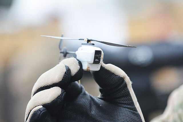
Harris & Harris Group, Inc. (Nasdaq: TINY), an investor in transformative companies enabled by disruptive science, notes that its portfolio company, D-Wave Systems, Inc., announced that it has successfully fabricated 1,000 qubit processors that power its quantum computers.  D-Wave’s quantum computer runs a quantum annealing algorithm to find the lowest points, corresponding to optimal or near optimal solutions, in a virtual “energy landscape.”  Every additional qubit doubles the search space of the processor.  At 1,000 qubits, the new processor considers 21000 possibilities simultaneously, a search space which is substantially larger than the 2512 possibilities available to the company’s currently available 512 qubit D-Wave Two. In fact, the new search space contains far more possibilities than there are particles in the observable universe.

A June 22, 2015 D-Wave news release, which originated the technical details about the breakthrough found in the Harris & Harris press release, provides more information along with some marketing hype (hyperbole), Note: Links have been removed,

As the only manufacturer of scalable quantum processors, D-Wave breaks new ground with every succeeding generation it develops. The new processors, comprising over 128,000 Josephson tunnel junctions, are believed to be the most complex superconductor integrated circuits ever successfully yielded. They are fabricated in part at D-Wave’s facilities in Palo Alto, CA and at Cypress Semiconductor’s wafer foundry located in Bloomington, Minnesota.

“Temperature, noise, and precision all play a profound role in how well quantum processors solve problems.  Beyond scaling up the technology by doubling the number of qubits, we also achieved key technology advances prioritized around their impact on performance,” said Jeremy Hilton, D-Wave vice president, processor development. “We expect to release benchmarking data that demonstrate new levels of performance later this year.”

The 1000-qubit milestone is the result of intensive research and development by D-Wave and reflects a triumph over a variety of design challenges aimed at enhancing performance and boosting solution quality. Beyond the much larger number of qubits, other significant innovations include:

  •  Lower Operating Temperature: While the previous generation processor ran at a temperature close to absolute zero, the new processor runs 40% colder. The lower operating temperature enhances the importance of quantum effects, which increases the ability to discriminate the best result from a collection of good candidates.​
  • Reduced Noise: Through a combination of improved design, architectural enhancements and materials changes, noise levels have been reduced by 50% in comparison to the previous generation. The lower noise environment enhances problem-solving performance while boosting reliability and stability.
  • Increased Control Circuitry Precision: In the testing to date, the increased precision coupled with the noise reduction has demonstrated improved precision by up to 40%. To accomplish both while also improving manufacturing yield is a significant achievement.
  • Advanced Fabrication:  The new processors comprise over 128,000 Josephson junctions (tunnel junctions with superconducting electrodes) in a 6-metal layer planar process with 0.25μm features, believed to be the most complex superconductor integrated circuits ever built.
  • New Modes of Use: The new technology expands the boundaries of ways to exploit quantum resources.  In addition to performing discrete optimization like its predecessor, firmware and software upgrades will make it easier to use the system for sampling applications.

“Breaking the 1000 qubit barrier marks the culmination of years of research and development by our scientists, engineers and manufacturing team,” said D-Wave CEO Vern Brownell. “It is a critical step toward bringing the promise of quantum computing to bear on some of the most challenging technical, commercial, scientific, and national defense problems that organizations face.”

A June 20, 2015 article in The Economist notes there is now commercial interest as it provides good introductory information about quantum computing. The article includes an analysis of various research efforts in Canada (they mention D-Wave), the US, and the UK. These excerpts don’t do justice to the article but will hopefully whet your appetite or provide an overview for anyone with limited time,

A COMPUTER proceeds one step at a time. At any particular moment, each of its bits—the binary digits it adds and subtracts to arrive at its conclusions—has a single, definite value: zero or one. At that moment the machine is in just one state, a particular mixture of zeros and ones. It can therefore perform only one calculation next. This puts a limit on its power. To increase that power, you have to make it work faster.

But bits do not exist in the abstract. Each depends for its reality on the physical state of part of the computer’s processor or memory. And physical states, at the quantum level, are not as clear-cut as classical physics pretends. That leaves engineers a bit of wriggle room. By exploiting certain quantum effects they can create bits, known as qubits, that do not have a definite value, thus overcoming classical computing’s limits.

… The biggest question is what the qubits themselves should be made from.

A qubit needs a physical system with two opposite quantum states, such as the direction of spin of an electron orbiting an atomic nucleus. Several things which can do the job exist, and each has its fans. Some suggest nitrogen atoms trapped in the crystal lattices of diamonds. Calcium ions held in the grip of magnetic fields are another favourite. So are the photons of which light is composed (in this case the qubit would be stored in the plane of polarisation). And quasiparticles, which are vibrations in matter that behave like real subatomic particles, also have a following.

The leading candidate at the moment, though, is to use a superconductor in which the qubit is either the direction of a circulating current, or the presence or absence of an electric charge. Both Google and IBM are banking on this approach. It has the advantage that superconducting qubits can be arranged on semiconductor chips of the sort used in existing computers. That, the two firms think, should make them easier to commercialise.

Google is also collaborating with D-Wave of Vancouver, Canada, which sells what it calls quantum annealers. The field’s practitioners took much convincing that these devices really do exploit the quantum advantage, and in any case they are limited to a narrower set of problems—such as searching for images similar to a reference image. But such searches are just the type of application of interest to Google. In 2013, in collaboration with NASA and USRA, a research consortium, the firm bought a D-Wave machine in order to put it through its paces. Hartmut Neven, director of engineering at Google Research, is guarded about what his team has found, but he believes D-Wave’s approach is best suited to calculations involving fewer qubits, while Dr Martinis and his colleagues build devices with more.

It’s not clear to me if the writers at The Economist were aware of  D-Wave’s latest breakthrough at the time of writing but I think not. In any event, they (The Economist writers) have included a provocative tidbit about quantum encryption,

Documents released by Edward Snowden, a whistleblower, revealed that the Penetrating Hard Targets programme of America’s National Security Agency was actively researching “if, and how, a cryptologically useful quantum computer can be built”. In May IARPA [Intellligence Advanced Research Projects Agency], the American government’s intelligence-research arm, issued a call for partners in its Logical Qubits programme, to make robust, error-free qubits. In April, meanwhile, Tanja Lange and Daniel Bernstein of Eindhoven University of Technology, in the Netherlands, announced PQCRYPTO, a programme to advance and standardise “post-quantum cryptography”. They are concerned that encrypted communications captured now could be subjected to quantum cracking in the future. That means strong pre-emptive encryption is needed immediately.

I encourage you to read the Economist article.

Two final comments. (1) The latest piece, prior to this one, about D-Wave was in a Feb. 6, 2015 posting about then new investment into the company. (2) A Canadian effort in the field of quantum cryptography was mentioned in a May 11, 2015 posting (scroll down about 50% of the way) featuring a profile of Raymond Laflamme, at the University of Waterloo’s Institute of Quantum Computing in the context of an announcement about science media initiative Research2Reality.

Europe’s search for raw materials and hopes for nanotechnology-enabled solutions

A Feb. 27, 2015 news item on Nanowerk highlights the concerns over the availability of raw materials and European efforts to address those concerns,

Critical raw materials’ are crucial to many European industries but they are vulnerable to scarcity and supply disruption. As such, it is vital that Europe develops strategies for meeting the demand for raw materials. One such strategy is finding methods or substances that can replace the raw materials that we currently use. With this in mind, four EU projects working on substitution in catalysis, electronics and photonics presented their work at the Third Innovation Network Workshop on substitution of Critical Raw Materials hosted by the CRM_INNONET project in Brussels earlier this month [February 2015].

A Feb. 26, 2015 CORDIS press release, which originated the news item, goes on to describe four European Union projects working on nanotechnology-enabled solutions,

NOVACAM

NOVACAM, a coordinated Japan-EU project, aims to develop catalysts using non-critical elements designed to unlock the potential of biomass into a viable energy and chemical feedstock source.

The project is using a ‘catalyst by design’ approach for the development of next generation catalysts (nanoscale inorganic catalysts), as NOVACAM project coordinator Prof. Emiel Hensen from Eindhoven University of Technology in the Netherlands explained. Launched in September 2013, the project is developing catalysts which incorporate non-critical metals to catalyse the conversion of lignocellulose into industrial chemical feedstocks and bio-fuels. The first part of the project has been to develop the principle chemistry while the second part is to demonstrate proof of process. Prof. Hensen predicts that perhaps only two of three concepts will survive to this phase.

The project has already made significant progress in glucose and ethanol conversion, according to Prof. Hensen, and has produced some important scientific publications. The consortium is working with and industrial advisory board comprising Shell in the EU and Nippon Shokubai in Japan.

FREECATS

The FREECATS project, presented by project coordinator Prof. Magnus Rønning from the Norwegian University of Science and Technology, has been working over the past three years to develop new metal-free catalysts. These would be either in the form of bulk nanomaterials or in hierarchically organised structures – both of which would be capable of replacing traditional noble metal-based catalysts in catalytic transformations of strategic importance.

Prof. Magnus Rønning explained that the application of the new materials could eliminate the need for the use for platinum group metals (PGM) and rare earth metals – in both cases Europe is very reliant on other countries for these materials. Over the course of its research, FREECATS targeted three areas in particular – fuel cells, the production of light olefins and water and wastewater purification.

By working to replace the platinum in fuel cells, the project is supporting the EU’s aim of replacing the internal combustion engine by 2050. However, as Prof. Rønning noted, while platinum has been optimized for use over several decades, the materials FREECATS are using are new and thus come with their new challenges which the project is addressing.

HARFIR

Prof. Atsufumi Hirohata of the University of York in the United Kingdom, project coordinator of HARFIR, described how the project aims to discover an antiferromagnetic alloy that does not contain the rare metal Iridium. Iridium is becoming more and more widely used in numerous spin electronic storage devices, including read heads in hard disk drives. The world supply depends on Platinum ore that comes mainly from South Africa. The situation is much worse than for other rare earth elements as the price has been shooting up over recent years, according to Prof. Hirohata.

The HARFIR team, divided between Europe and Japan, aims to replace Iridium alloys with Heusler alloys. The EU team, led by Prof. Hirohata, has been working on the preparation of polycrystalline and epitaxial thin films of Heusler Alloys, with the material design led by theoretical calculations. The Japanese team, led by Prof. Koki Takanashi at Tohoku University, is meanwhile working on the preparation of epitaxial thin films, measurements of fundamental properties and structural/magnetic characterisation by neutron and synchrotron x-ray beams.

One of the biggest challenges has been that Heusler alloys have a relatively complicated atomic structure. In terms of HARFIR’s work, if any atomic disordering at the edge of nanopillar devices, the magnetic properties that are needed are lost. The team is exploring solutions to this challenge.

IRENA

Prof. of Esko Kauppinen Aalto University in Finland closed off the first session of the morning with his presentation of the IRENA project. Launched in September 2013, the project will run until mid 2017 working towards the aim of developing high performance materials, specifically metallic and semiconducting single-walled carbon nanotube (SWCNT) thin films to completely eliminate the use of the critical metals in electron devices. The ultimate aim is to replace Indium in transparent conducting films, and Indium and Gallium as a semiconductor in thin film field effect transistors (TFTs).

The IRENA team is developing an alternative that is flexible, transparent and stretchable so that it can meet the demands of the electronics of the future – including the possibility to print electronics.

IRENA involves three partners from Europe and three from Japan. The team has expertise in nanotube synthesis, thin film manufacturing and flexible device manufacturing, modelling of nanotube growth and thin film charge transport processes, and the project has benefitted from exchanges of team members between institutions. One of the key achievements so far is that the project has succeeded in using a nanotube thin film for the first time as the both the electrode and hole blocking layer in an organic solar cell.

You’ll note that Japan is a partner in all of these projects. In all probability, these initiatives have something to do with rare earths which are used in much of today’s electronics technology and Japan is sorely lacking in those materials. China, by comparison, has dominated the rare earths export industry and here’s an excerpt from my Nov. 1, 2013 posting where I outline the situation (which I suspect hasn’t changed much since),

As for the short supply mentioned in the first line of the news item, the world’s largest exporter of rare earth elements at 90% of the market, China, recently announced a cap according to a Sept. 6, 2013 article by David Stanway for Reuters. The Chinese government appears to be curtailing exports as part of an ongoing, multi-year strategy. Here’s how Cientifica‘s (an emerging technologies consultancy, etc.) white paper (Simply No Substitute?) about critical materials published in 2012 (?), described the situation,

Despite their name, REE are not that rare in the Earth’s crust. What has happened in the past decade is that REE exports from China undercut prices elsewhere, leading to the closure of mines such as the Mountain Pass REE mine in California. Once China had acquired a dominant market position, prices began to rise. But this situation will likely ease. The US will probably begin REE production from the Mountain Pass mine later in 2012, and mines in other countries are expected to start operation soon as well.

Nevertheless, owing to their broad range of uses REE will continue to exert pressures on their supply – especially for countries without notable REE deposits. This highlights two aspects of importance for strategic materials: actual rarity and strategic supply issues such as these seen for REE. Although strategic and diplomatic supply issues may have easier solutions, their consideration for manufacturing industries will almost be the same – a shortage of crucial supply lines.

Furthermore, as the example of REE shows, the identification of long-term supply problems can often be difficult, and not every government has the same strategic foresight that the Chinese demonstrated. And as new technologies emerge, new elements may see an unexpected, sudden demand in supply. (pp. 16-17)

Meanwhile, in response to China’s decision to cap its 2013 REE exports, the Russian government announced a $1B investment to 2018 in rare earth production,, according to a Sept. 10, 2013 article by Polina Devitt for Reuters.

I’m not sure you’ll be able to access Tim Harper’s white paper as he is now an independent, serial entrepreneur. I most recently mentioned him in relation to his articles (on Azonano) about the nanotechnology scene in a Feb. 12, 2015 posting where you’ll also find contact details for him.

Could there be a quantum internet?

We’ve always had limited success with predicting future technologies by examining current technologies. For example, the Internet and World Wide Web as we experience them today would have been unthinkable for most people in the 1950s when computers inhabited entire buildings and satellites were a brand new technology designed for space exploration not bouncing communication signals around the planet. That said, this new work on a ‘quantum internet’ from Eindhoven University of Technology is quite intriguing (from a Dec. 15, 2014 news item on Nanowerk),

In the same way as we now connect computers in networks through optical signals, it could also be possible to connect future quantum computers in a ‘quantum internet’. The optical signals would then consist of individual light particles or photons. One prerequisite for a working quantum internet is control of the shape of these photons. Researchers at Eindhoven University of Technology (TU/e) and the FOM foundation  [Foundation for Fundamental Research on Matter] have now succeeded for the first time in getting this control within the required short time.

A Dec. 15, 2014 Eindhoven University of Technology (TU/e) press release, which originated the news item, describes one of the problems with a ‘quantum internet’ and the researchers’ solution,

Quantum computers could in principle communicate with each other by exchanging individual photons to create a ‘quantum internet’. The shape of the photons, in other words how their energy is distributed over time, is vital for successful transmission of information. This shape must be symmetric in time, while photons that are emitted by atoms normally have an asymmetric shape. Therefore, this process requires external control in order to create a quantum internet.

Optical cavity

Researchers at TU/e and FOM have succeeded in getting the required degree of control by embedding a quantum dot – a piece of semiconductor material that can transmit photons – into a ‘photonic crystal’, thereby creating an optical cavity. Then the researchers applied a very short electrical pulse to the cavity, which influences how the quantum dot interacts with it, and how the photon is emitted. By varying the strength of this pulse, they were able to control the shape of the transmitted photons.

Within a billionth of a second

The Eindhoven researchers are the first to achieve this, thanks to the use of electrical pulses shorter than nanosecond, a billionth of a second. This is vital for use in quantum communication, as research leader Andrea Fiore of TU/e explains: “The emission of a photon only lasts for one nanosecond, so if you want to change anything you have to do it within that time. It’s like the shutter of a high-speed camera, which has to be very short if you want to capture something that changes very fast in an image. By controlling the speed at which you send a photon, you can in principle achieve very efficient exchange of photons, which is important for the future quantum internet.”

Here’s a link to and a citation for the paper,

Dynamically controlling the emission of single excitons in photonic crystal cavities by Francesco Pagliano, YongJin Cho, Tian Xia, Frank van Otten, Robert Johne, & Andrea Fiore. Nature Communications 5, Article number: 5786 doi:10.1038/ncomms6786 Published 15 December 2014

This is an open access paper.

ETA Dec. 16, 2014 at 1230 hours PDT: There is a copy of the Dec. 15, 2014 news release on EurekAlert.

Hummingbirds and ‘nano’ spy cameras

Hummingbird-inspired spy cameras have come a long way since the research featured in this Aug. 12, 2011 posting which includes a video of a robot camera designed to look like a hummingbird and mimic some of its extraordinary flying abilities. These days (2014) the emphasis appears to be on mimicking the abilities to a finer degree if Margaret Munro’s July 29, 2014 article for Canada.com is to be believed,

Tiny, high-end military drones are catching up with one of nature’s great engineering masterpieces.

A side-by-side comparison has found a “remarkably similar” aerodynamic performance between hummingbirds and the Black Hornet, the most sophisticated nano spycam yet.

“(The) Average Joe hummingbird” is about on par with the tiny helicopter that is so small it can fit in a pocket, says engineering professor David Lentink, at Stanford University. He led a team from Canada [University of British Columbia], the U.S. and the Netherlands [Wageningen University and Eindhoven University of Technology] that compared the birds and the machine for a study released Tuesday [July 29, 2014].

For a visual comparison with the latest nano spycam (Black Hornet), here’s the ‘hummingbird’ featured in the 2011 posting,

The  Nano Hummingbird, a drone from AeroVironment designed for the US Pentagon, would fit into any or all of those categories.

And, here’s this 2013 image of a Black Hornet Nano Helicopter inspired by hummingbirds,

Black Hornet Nano Helicopter UAVView licenseview terms Richard Watt - Photo http://www.defenceimagery.mod.uk/fotoweb/fwbin/download.dll/45153802.jpgCourtesy: Wikipedia

Black Hornet Nano Helicopter UAVView licenseview terms
Richard Watt – Photo http://www.defenceimagery.mod.uk/fotoweb/fwbin/download.dll/45153802.jpg Courtesy: Wikipedia

A July 30, 2014 Stanford University news release by Bjorn Carey provides more details about this latest research into hummingbirds and their flying ways,

More than 42 million years of natural selection have turned hummingbirds into some of the world’s most energetically efficient flyers, particularly when it comes to hovering in place.

Humans, however, are gaining ground quickly. A new study led by David Lentink, an assistant professor of mechanical engineering at Stanford, reveals that the spinning blades of micro-helicopters are about as efficient at hovering as the average hummingbird.

The experiment involved spinning hummingbird wings – sourced from a pre-existing museum collection – of 12 different species on an apparatus designed to test the aerodynamics of helicopter blades. The researchers used cameras to visualize airflow around the wings, and sensitive load cells to measure the drag and the lift force they exerted, at different speeds and angles.

Lentink and his colleagues then replicated the experiment using the blades from a ProxDynamics Black Hornet autonomous microhelicopter. The Black Hornet is the most sophisticated microcopter available – the United Kingdom’s army uses it in Afghanistan – and is itself about the size of a hummingbird.

Even spinning like a helicopter, rather than flapping, the hummingbird wings excelled: If hummingbirds were able to spin their wings to hover, it would cost them roughly half as much energy as flapping. The microcopter’s wings kept pace with the middle-of-the-pack hummingbird wings, but the topflight wings – those of Anna’s hummingbird, a species common throughout the West Coast – were still about 27 percent more efficient than engineered blades.

Hummingbirds acing the test didn’t particularly surprise Lentink – previous studies had indicated hummingbirds were incredibly efficient – but he was impressed with the helicopter.

“The technology is at the level of an average Joe hummingbird,” Lentink said. “A helicopter is really the most efficient hovering device that we can build. The best hummingbirds are still better, but I think it’s amazing that we’re getting closer. It’s not easy to match their performance, but if we build better wings with better shapes, we might approximate hummingbirds.”

Based on the measurements of Anna’s hummingbirds, Lentink said there is potential to improve microcopter rotor power by up to 27 percent.

The high-fidelity experiment also provided an opportunity to refine previous rough estimates of muscle power. Lentink’s team learned that hummingbirds’ muscles produce a surprising 130 watts of energy per kilogram; the average for other birds, and across most vertebrates, is roughly 100 watts/kg.

Although the current study revealed several details of how a hummingbird hovers in one place, the birds still hold many secrets. For instance, Lentink said, we don’t know how hummingbirds maintain their flight in a strong gust, how they navigate through branches and other clutter, or how they change direction so quickly during aerial “dogfights.”

He also thinks great strides could be made by studying wing aspect ratios, the ratio of wing length to wing width. The aspect ratios of all the hummingbirds’ wings remarkably converged around 3.9. The aspect ratios of most wings used in aviation measure much higher; the Black Hornet’s aspect ratio was 4.7.

“I want to understand if aspect ratio is special, and whether the amount of variation has an effect on performance,” Lentink said. Understanding and replicating these abilities and characteristics could be a boon for robotics and will be the focus of future experiments.

“Those are the things we don’t know right now, and they could be incredibly useful. But I don’t mind it, actually,” Lentink said. “I think it’s nice that there are still a few things about hummingbirds that we don’t know.”

Agreed, it’s nice to know there are still a few mysteries left. You can watch the ‘mysterious’ hummingbird in this video courtesy of the Rivers Ingersoll Lentink Lab at Stanford University,

High speed video of Anna’s hummingbird at Stanford Arizona Cactus Garden.

Here’s a link to and a citation for the paper, H/T to Nancy Owano’s article on phys.org for alerting me to this story.

Hummingbird wing efficacy depends on aspect ratio and compares with helicopter rotors by Jan W. Kruyt, Elsa M. Quicazán-Rubio, GertJan F. van Heijst, Douglas L. Altshuler, and David Lentink.  J. R. Soc. Interface 6 October 2014 vol. 11 no. 99 20140585 doi: 10.1098/​rsif.2014.0585 Published [online] 30 July 2014

This is an open access paper.

Despite Munro’s reference to the Black Hornet as a ‘nano’ spycam, the ‘microhelicopter’ description in the news release places the device at the microscale (/1,000,000,000). Still, I don’t understand what makes it microscale since it’s visible to the naked eye. In any case, it is small.

RoboEarth (robot internet) gets examined in hospital

RoboEarth sometimes referred to as a robot internet or a robot world wide web is being tested this week by a team of researchers at Eindhoven University of Technology (Technische Universiteit Eindhoven, Netherlands) and their colleagues at Philips, ETH Zürich, TU München and the universities of Zaragoza and Stuttgart according to a Jan. 14, 2014 news item on BBC (British Broadcasting Corporation) news online,

A world wide web for robots to learn from each other and share information is being shown off for the first time.

Scientists behind RoboEarth will put it through its paces at Eindhoven University in a mocked-up hospital room.

Four robots will use the system to complete a series of tasks, including serving drinks to patients.

It is the culmination of a four-year project, funded by the European Union.

The eventual aim is that both robots and humans will be able to upload information to the cloud-based database, which would act as a kind of common brain for machines.

There’s a bit more detail in Victoria Turk’s Jan. 13 (?), 2014 article for motherboard.vice.com (Note: A link has been removed),

A hospital-like setting is an ideal test for the project, because where RoboEarth could come in handy is in helping out humans with household tasks. A big problem for robots at the moment is that human environments tend to change a lot, whereas robots are limited to the very specific movements and tasks they’ve been programmed to do.

“To enable robots to successfully lend a mechanical helping hand, they need to be able to deal flexibly with new situations and conditions,” explains a post by the University of Eindhoven. “For example you can teach a robot to bring you a cup of coffee in the living room, but if some of the chairs have been moved the robot won’t be able to find you any longer. Or it may get confused if you’ve just bought a different set of coffee cups.”

And of course, it wouldn’t just be limited to robots working explicitly together. The Wikipedia-like knowledge base is more like an internet for machines, connecting lonely robots across the globe.

A Jan. 10, 2014 Eindhoven University of Technology news release provides some insight into what the researchers want to accomplish,

“The problem right now is that robots are often developed specifically for one task”, says René van de Molengraft, TU/e  [Eindhoven University of Technology] researcher and RoboEarth project leader. “Everyday changes that happen all the time in our environment make all the programmed actions unusable. But RoboEarth simply lets robots learn new tasks and situations from each other. All their knowledge and experience are shared worldwide on a central, online database. As well as that, computing and ‘thinking’ tasks can be carried out by the system’s ‘cloud engine’, so the robot doesn’t need to have as much computing or battery power on‑board.”

It means, for example, that a robot can image a hospital room and upload the resulting map to RoboEarth. Another robot, which doesn’t know the room, can use that map on RoboEarth to locate a glass of water immediately, without having to search for it endlessly. In the same way a task like opening a box of pills can be shared on RoboEarth, so other robots can also do it without having to be programmed for that specific type of box.

There’s no word as to exactly when this test being demonstrated to a delegation from the European Commission, which financed the project, using four robots and two simulated hospital rooms is being held.

I first wrote about* RoboEarth in a Feb. 14, 2011 posting (scroll down about 1/4 of the way) and again in a March 12 2013 posting about the project’s cloud engine, Rapyuta.

* ‘abut’ corrected to ‘about’ on Sept. 2, 2014.

Archivists, rejoice! Fused quartz stores data for millions of years at the University of Southampton (UK)

There’s a July 9,  2013 news item on Nanowerk touting nanostructured glass device which is being compared to Superman’s memory crystal (see this Wikipedia essay on Superman’s Fortress of Solitude for a description of Superman’s memory crystals),

Using nanostructured glass, scientists at the University of Southampton have, for the first time, experimentally demonstrated the recording and retrieval processes of five dimensional digital data by femtosecond laser writing. The storage allows unprecedented parameters including 360 TB/disc data capacity, thermal stability up to 1000°C and practically unlimited lifetime.

Coined as the ‘Superman’ memory crystal, as the glass memory has been compared to the “memory crystals” used in the Superman films, the data is recorded via self-assembled nanostructures created in fused quartz, which is able to store vast quantities of data for over a million years. The information encoding is realised in five dimensions: the size and orientation in addition to the three dimensional position of these nanostructures. [emphases mine]

The July 9, 2013 University of Southampton news release, which originated the news item, provides more details,

A 300 kb digital copy of a text file was successfully recorded in 5D using ultrafast laser, producing extremely short and intense pulses of light. The file is written in three layers of nanostructured dots separated by five micrometres (one millionth of a metre).

The self-assembled nanostructures change the way light travels through glass, modifying polarisation of light that can then be read by combination of optical microscope and a polariser, similar to that found in Polaroid sunglasses.

The research is led by Jingyu Zhang from the University’s Optoelectronics Research Centre (ORC) and conducted under a joint project with Eindhoven University of Technology.

“We are developing a very stable and safe form of portable memory using glass, which could be highly useful for organisations with big archives. At the moment companies have to back up their archives every five to ten years because hard-drive memory has a relatively short lifespan,” says Jingyu. [emphasis mine]

“Museums who want to preserve information or places like the national archives where they have huge numbers of documents, would really benefit.”

This work was presented at the CLEO 2013 (Conference on Lasers and Electro-Optics in San Jose [US]). Here’s a link to and a citation for the 2 pp presentation paper,

5D Data Storage by Ultrafast Laser Nanostructuring in Glass by Jingyu Zhang, Mindaugas Gecevičius, Martynas Beresna, and Peter G. Kazansky. Presentation paper for CLEO 2013

© 2013 Optical Society of America OCIS codes (140.3390) Laser materials processing, (210.0210) Optical data storage

This research was conducted as part of the European Union’s Femtoprint project, which is funded under the Framework Programme 7 initiative. Here’s more about Femtoprint from the homepage,

FEMTOPRINT is to develop a printer for microsystems with nano-scale features fabricated out of glass. Our ultimate goal is to provide a large pool of users from industry, research and universities with the capability of producing their own micro-systems, in a rapid-manner without the need for expensive infrastructures and specific expertise. Recent researches have shown that one can form three-dimensional patterns in glass material using low-power femtosecond laser beam. This simple process opens interesting new opportunities for a broad variety of microsystems with feature sizes down to the nano-scale. These patterns can be used to form integrated optics components or be ‘developed’ by chemically etching to form three-dimensional structures like fluidic channels and micro-mechanical components. Worth noticing, sub-micron resolution can be achieved and sub-pattern smaller than the laser wavelength can be formed. Thanks to the low-energy required to pattern the glass, femtosecond laser consisting simply of an oscillator are sufficient to produce such micro- and nano- systems.

These systems are nowadays table-top and cost a fraction of conventional clean-room equipments. It is highly foreseeable that within 3 to 5 years such laser systems will fit in a shoe-box. The project specific objectives are:

1/ Develop a femtosecond laser suitable for glass micro-/nano- manufacturing that fits in a shoe-box

2/ Integrate the laser in a machine similar to a printer that can position and manipulate glass sheets of various thicknesses

3/ Demonstrate the use of the printer to fabricate a variety of micro-/nano-systems with optical, mechanical and fluid-handling capabilities. A clear and measurable outcome of Femtoprint will be to be in a situation to commercialize the ‘femtoprinter’ through the setting-up of a consortium spin-off. The potential economical impact is large and is expected in various industrial sectors.

I think any archivist hearing about data storage that can last a million years will be thrilled although I suspect it’s going to be a long, long time before these 5D ‘memory’ crystals are going to be storing any data for anyone. In the meantime, there are efforts such as the Council of Canadian Academies’ (CCA) Memory Institutions and the Digital Revolution assessment (mentioned 2/3 of the way down in my June 5, 2013 posting).