Tag Archives: electromagnetic fields

Taking spectroscopy to a new dimension with silver nanoparticles

This latest move towards better detection at the nanoscale comes from India (from a January 2, 2018 news item on ScienceDaily),

As medicine and pharmacology investigate nanoscale processes, it has become increasingly important to identify and characterize different molecules. Raman spectroscopy, a technique that leverages the scattering of laser light to identify molecules, has a limited capacity to detect molecules in diluted samples because of low signal yield.

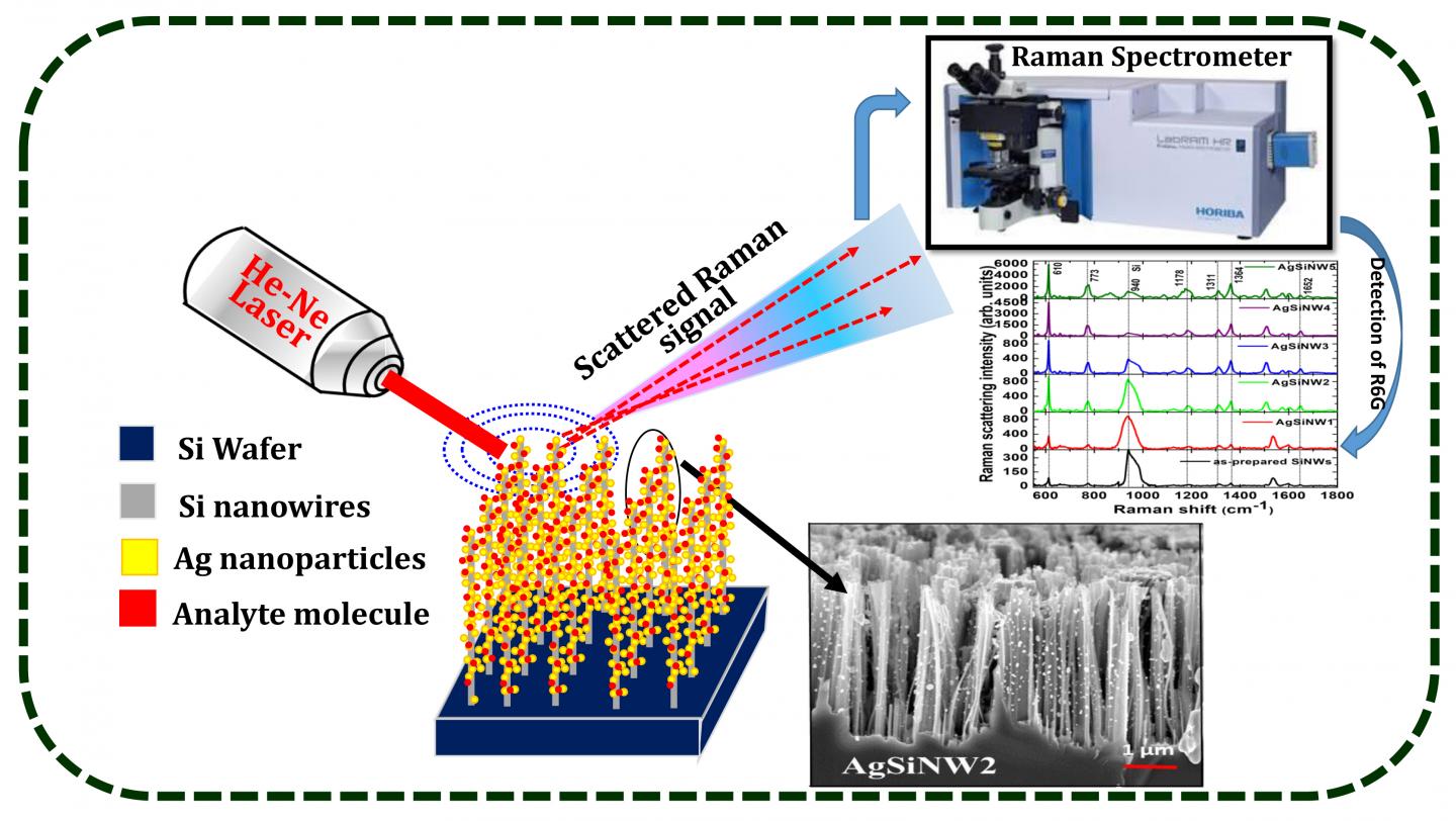
A team of researchers from the University of Hyderabad in India has improved molecular detection at low concentration levels by arranging nanoparticles on nanowires to enhance Raman spectroscopy. Surface-enhanced Raman spectroscopy (SERS) uses electromagnetic fields to improve Raman scattering and boost sensitivity in standard dyes such as R6G by more than one billionfold.

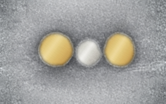
Here’s an image illustrating the work,

Caption: Detection of a low concentration analyte molecule using silicon nanowires decorated with silver nanoparticles and surface enhanced Raman scattering measurements. Credit: V.S. Vendamani

A January 2, 2017 American Institute of Physics press release on EurekAlert, which originated the news item, explains further,

The team decorated vertically aligned silicon nanowires with varying densities of silver nanoparticles, utilizing and enhancing the structure’s 3-D shape. Their results, published in the Journal of Applied Physics, from AIP [American Institute of Physics] Publishing, show that their device was able to enhance the Raman signals for cytosine protein and ammonium perchlorate by a factor of 100,000.

“The beauty is that we can improve the density of these nanowires using simple chemistry,” said Soma Venugopal Rao, one of the paper’s authors. “If you have a large density of nanowires, you can put more silver nanoparticles into the substrate and can increase the sensitivity of the substrate.”

Applying the necessary nanostructures to SERS devices remains a challenge for the field. Building these structures in three dimensions with silicon nanowires has garnered attention for their higher surface area and superior performance, but silicon nanowires are still expensive to produce.

Instead, the team was able to find a cheaper way to make silicon nanowires and used a technique called electroless etching to make a wide range of nanowires. They “decorated” these wires with silver nanoparticles with variable and controlled densities, which increased the nanowires’ surface area.

“Optimizing these vertically aligned structures took a lot of time in the beginning,” said Nageswara Rao, another of the paper’s authors. “We increased the surface area and to do this we needed to change the aspect ratio.”

After optimizing their system to detect Rhodamine dye on a nanomolar level, these new substrates the team built enhanced Raman sensitivity by a factor of 10,000 to 100,000. The substrates detected concentrations of cytosine, a nucleotide found in DNA, and ammonium perchlorate, a molecule with potential for detecting explosives, in as dilute concentrations as 50 and 10 micromolar, respectively.

The results have given the team reason to believe that it might soon be possible to detect compounds in concentrations on the scale of nanomolar or even picomolar, Nageswara Rao said. The team’s work has opened several avenues for future research, from experimenting with different nanoparticles such as gold, increasing the sharpness of the nanowires or testing these devices across several types of molecules.

Here’s a link to and a citation for the paper,

Three-dimensional hybrid silicon nanostructures for surface enhanced Raman spectroscopy based molecular detection featured by V. S. Vendamani, S. V. S. Nageswara Rao, S. Venugopal Rao, D. Kanjilal, and A. P. Pathak. Journal of Applied Physics 123, 014301 (2018); Published Online: January 2018 https://doi.org/10.1063/1.5000994

This paper is open access.

Light-based computation made better with silver

It’s pretty amazing to imagine a future where computers run on light but according to a May 16, 2017 news item on ScienceDaily the idea is not beyond the realms of possibility,

Tomorrow’s computers will run on light, and gold nanoparticle chains show much promise as light conductors. Now Ludwig-Maximilians-Universitaet (LMU) in Munich scientists have demonstrated how tiny spots of silver could markedly reduce energy consumption in light-based computation.

Today’s computers are faster and smaller than ever before. The latest generation of transistors will have structural features with dimensions of only 10 nanometers. If computers are to become even faster and at the same time more energy efficient at these minuscule scales, they will probably need to process information using light particles instead of electrons. This is referred to as “optical computing.”

The silver serves as a kind of intermediary between the gold particles while not dissipating energy. Capture: Liedl/Hohmann (NIM)

A March 15, 2017 LMU press release (also one EurekAlert), which originated the news item, describes a current use of light in telecommunications technology and this latest research breakthrough (the discrepancy in dates is likely due to when the paper was made available online versus in print),

Fiber-optic networks already use light to transport data over long distances at high speed and with minimum loss. The diameters of the thinnest cables, however, are in the micrometer range, as the light waves — with a wavelength of around one micrometer — must be able to oscillate unhindered. In order to process data on a micro- or even nanochip, an entirely new system is therefore required.

One possibility would be to conduct light signals via so-called plasmon oscillations. This involves a light particle (photon) exciting the electron cloud of a gold nanoparticle so that it starts oscillating. These waves then travel along a chain of nanoparticles at approximately 10% of the speed of light. This approach achieves two goals: nanometer-scale dimensions and enormous speed. What remains, however, is the energy consumption. In a chain composed purely of gold, this would be almost as high as in conventional transistors, due to the considerable heat development in the gold particles.

A tiny spot of silver

Tim Liedl, Professor of Physics at LMU and PI at the cluster of excellence Nanosystems Initiative Munich (NIM), together with colleagues from Ohio University, has now published an article in the journal Nature Physics, which describes how silver nanoparticles can significantly reduce the energy consumption. The physicists built a sort of miniature test track with a length of around 100 nanometers, composed of three nanoparticles: one gold nanoparticle at each end, with a silver nanoparticle right in the middle.

The silver serves as a kind of intermediary between the gold particles while not dissipating energy. To make the silver particle’s plasmon oscillate, more excitation energy is required than for gold. Therefore, the energy just flows “around” the silver particle. “Transport is mediated via the coupling of the electromagnetic fields around the so-called hot spots which are created between each of the two gold particles and the silver particle,” explains Tim Liedl. “This allows the energy to be transported with almost no loss, and on a femtosecond time scale.”

Textbook quantum model

The decisive precondition for the experiments was the fact that Tim Liedl and his colleagues are experts in the exquisitely exact placement of nanostructures. This is done by the DNA origami method, which allows different crystalline nanoparticles to be placed at precisely defined nanodistances from each other. Similar experiments had previously been conducted using conventional lithography techniques. However, these do not provide the required spatial precision, in particular where different types of metals are involved.

In parallel, the physicists simulated the experimental set-up on the computer – and had their results confirmed. In addition to classical electrodynamic simulations, Alexander Govorov, Professor of Physics at Ohio University, Athens, USA, was able to establish a simple quantum-mechanical model: “In this model, the classical and the quantum-mechanical pictures match very well, which makes it a potential example for the textbooks.”

Here’s a link to and c citation for the paper,

Hotspot-mediated non-dissipative and ultrafast plasmon passage by Eva-Maria Roller, Lucas V. Besteiro, Claudia Pupp, Larousse Khosravi Khorashad, Alexander O. Govorov, & Tim Liedl. Nature Physics (2017) doi:10.1038/nphys4120 Published online 15 May 2017

This paper is behind a paywall.