Tag Archives: electronics

Phagocytosis for a bioelectronic future

The process by which a cell engulfs matter is known as phagocytosis. One of the best known examples of failed phagocytosis is that of asbestos fibres in the lungs where lung cells have attempted to engulf a fibre that’s just too big and ends up piercing the cell. When enough of the cells are pierced, the person is diagnosed with mesothelioma.

This particular example of phagocytosis is a happier one according to a Dec. 16, 2016 article by Meghan Rosen for ScienceNews,

Human cells can snack on silicon.

Cells grown in the lab devour nano-sized wires of silicon through an engulfing process known as phagocytosis, scientists report December 16 in Science Advances.

Silicon-infused cells could merge electronics with biology, says John Zimmerman, a biophysicist now at Harvard University. “It’s still very early days,” he adds, but “the idea is to get traditional electronic devices working inside of cells.” Such hybrid devices could one day help control cellular behavior, or even replace electronics used for deep brain stimulation, he says.

Scientists have been trying to load electronic parts inside cells for years. One way is to zap holes in cells with electricity, which lets big stuff, like silicon nanowires linked to bulky materials, slip in. Zimmerman, then at the University of Chicago, and colleagues were looking for a simpler technique, something that would let tiny nanowires in easily and could potentially allow them to travel through a person’s bloodstream — like a drug.

A Dec. 22, 2016 University of Chicago news release by Matt Wood provides more detail,

“You can treat it as a non-genetic, synthetic biology platform,” said Bozhi Tian, PhD, assistant professor of chemistry and senior author of the new study. “Traditionally in biology we use genetic engineering and modify genetic parts. Now we can use silicon parts, and silicon can be internalized. You can target those silicon parts to specific parts of the cell and modulate that behavior with light.”

In the new study, Tian and his team show how cells consume or internalize the nanowires through phagocytosis, the same process they use to engulf and ingest nutrients and other particles in their environment. The nanowires are simply added to cell media, the liquid solution the cells live in, the same way you might administer a drug, and the cells take it from there. Eventually, the goal would be to inject them into the bloodstream or package them into a pill.

Once inside, the nanowires can interact directly with individual parts of the cell, organelles like the mitochondria, nucleus and cytoskeletal filaments. Researchers can then stimulate the nanowires with light to see how individual components of the cell respond, or even change the behavior of the cell. They can last up to two weeks inside the cell before biodegrading.

Seeing how individual parts of a cell respond to stimulation could give researchers insight into how medical treatments that use electrical stimulation work at a more detailed level. For instance, deep brain stimulation helps treat tremors from movement disorders like Parkinson’s disease by sending electrical signals to areas of the brain. Doctors know it works at the level of tissues and brain structures, but seeing how individual components of nerve cells react to these signals could help fine tune and improve the treatment.

The experiments in the study used umbilical vascular endothelial cells, which make up blood vessel linings in the umbilical cord. These cells readily took up the nanowires, but others, like cardiac muscle cells, did not. Knowing that some cells consume the wires and some don’t could also prove useful in experimental settings and give researchers more ways to target specific cell types.

Tian and his team manufactures the nanowires in their lab with a chemical vapor deposition system that grows the silicon structures to different specifications. They can adjust size, shape, and electrical properties as needed, or even add defects on purpose for testing. They can also make wires with porous surfaces that could deliver drugs or genetic material to the cells. The process gives them a variety of ways to manipulate the properties of the nanowires for research.

Here’s a link to and a citation for the paper,

Cellular uptake and dynamics of unlabeled freestanding silicon nanowires by John F. Zimmerman, Ramya Parameswaran, Graeme Murray, Yucai Wang, Michael Burke, and Bozhi Tian. Science Advances  16 Dec 2016: Vol. 2, no. 12, e1601039 DOI: 10.1126/sciadv.1601039

This paper appears to be open access.
Honey, could you please unzip my electronics?

The UK’s National Physical Laboratory has been proceeding with an interesting project on reusable electronics, ReUSE (Reuseable, Unzippable, Sustainable Electronics), according to the Oct. 30, 2012 news item on Nanowerk,

The National Physical Laboratory (NPL), along with partners In2Tec Ltd (UK) and Gwent Electronic Materials Ltd, have developed a printed circuit board (PCB) whose components can be easily separated by immersion in hot water. …

The electronics industry has a waste problem – currently over 100 million electronic units are discarded annually in the UK alone, making it one of the fastest growing waste streams.


It was estimated in a DTI [Dept. of Trade and Industry]-funded report, that around 85% of all PCB scrap board waste goes to landfill. Around 70% of this being of non-metallic content with little opportunity for recycling. This amounts to around 1 million tonnes in the UK annually equivalent to 81 x HMS Belfasts [ships]

This revolutionary materials technology allows a staggering 90% of the original structure to be re-used. For comparison, less than 2% of traditional PCB material can be re-used. The developed technology lends itself readily to rigid, flexible and 3D structures, which will enable the electronics industry to pursue new design philosophies – with the emphasis on using less materials and improving sustainability.

Here’s a video demonstrating the technology, from the ReUSE project news page,

I had to look at this twice to confirm what I was seeing. (I worked for a company that manufactured circuit boards for its products and the idea of immersing one of those in hot water is pretty shocking to me [pun intended].)

Rare earths, China, and Nanosys

There’s been some discussion recently about rare earths in the light of tensions between China and Japan. Here’s a brief description of rare earths for anyone who’s not certain what they are, from the Wikipedia essay on rare earths,

… rare earth elements or rare earth metals are a collection of seventeen chemical elements in the periodic table, namely scandium, yttrium, and the fifteen lanthanides.

Despite their name, rare earth elements (with the exception of the highly unstable promethium) are relatively plentiful in the Earth’s crust, with cerium being the 25th most abundant element at 68 parts per million (similar to copper). However, because of their geochemical properties, rare earth elements are not often found in concentrated and economically exploitable forms, generally called rare earth minerals. It was the very scarcity of these minerals (previously called “earths”) that led to the term “rare earth”

Here’s what started the tensions (from the NY Times article by Keith Bradsher),

Chinese customs officials abruptly halted the processing of paperwork for shipments bound for Japan on Sept. 21 [2010]. The shipments were halted during an acrimonious dispute over Japan’s detention of a Chinese fishing trawler that rammed two Japanese coast guard vessels two weeks earlier near islands long controlled by Japan but claimed by China.

Here’s why they’re so important,

Rare earths are vital to the production of a wide range of industrial products, including automobiles, glass, oil refining, computers, smartphones, wind turbines and flat-screen televisions. The military needs them for missiles, sonar systems and the range finders of tanks.

Here are some of the consequences of the ban,

Many factories in China assemble products that require high-tech components from Japan that use rare earths. Some of these factories, which employ large numbers of workers in China, have begun running low on components as Japanese suppliers ran short on some of the more obscure rare earths needed to manufacture them, two rare earth industry executives said.

Electronics industries have been affected, particularly camera manufacturers, leading to a desperate scramble for raw materials that has even included buying tons of obscure rare earth compounds from corporate stockpiles in Europe and airlifting them to Japan.

All 32 of the authorized rare earth exporters in China have refused to increase their shipments to other countries during the unannounced ban on shipments to Japan, making it difficult for Japanese traders to obtain supplies indirectly.

As a result of the blocked shipments, some rare earths now cost up to 10 times as much outside China as inside; the Chinese government has started a vigorous campaign to prevent this from leading to smuggling.

Brasher’s article is very interesting and I do recommend reading all of it.

There has been one other consequence to this concern over a dependency on China’s rare earths (excerpted from the Nov. 23, 2010 article by Ariel Schwartz on Fast Company),

There’s just one problem: The metals are only found in high concentrations in a few sites in China, the U.S., and Australia–and China has threatened to stop exporting its supply. But instead of expanding rare earth metal mines, what if we look for more sustainable replacements?

Enter Nanosys, a company that offers process-ready materials for the LED and energy-storage markets, among other things. Nanosys has been thinking about rare earth material shortages for years, which is why the company manufactures synthetic phosphors out of common materials–not the rare earth materials (i.e. yttrium) usually used in phosphors.

“We make a semiconductor phosphor that employs a nanomaterial called a quantum dot,” explains Nanosys CEO Jason Hartlove. “It’s made out of indium phosphide and phosphorous, and the synthesis process is all in the lab. There’s no heavy metal mining, no destructive mining practices.”

Nanosys’s QuantumRail LED backlighting device is made out of quantum dots, which can purportedly generate brighter and richer colors than their rare earth metal counterparts–all while delivering a higher efficiency and lower cost.

I don’t know how close they are to producing these quantum dots in industrial quantities but the appeal of a process that lessens dependency on resources that have to be mined and/or be used to apply political pressure is undeniable. If you’re interested, you can visit the Nanosys website here.

(They talk about ‘architected’ materials. I view that word with the same enthusiasm I have for ‘impactful’. These people should never be allowed to invent another word, ever again.)

Telecommunications through chemistry?

This isn’t intended to replace the use of electronics to transmit information but the work that George Whitesides and colleagues at Harvard University have just published (in Angewandte Chemie) is stunning to me.  From the news item on physorg.com,

We currently transmit information electronically; in the future we will most likely use photons. However, these are not the only alternatives. Information can also be transmitted by means of chemical reactions. George M. Whitesides and his colleagues at Harvard University in Cambridge have now developed a concept that allows transmission of alphanumeric information in the form of light pulses with no electricity: the “infofuse”.

Transmitting information by a chemical reaction? This is how the researchers approached the problem initially,

The strips were covered with patterns of dots made of salts of the elements lithium, rubidium, and cesium. When the strip is ignited, the flame travels forward and reaches the dots one after the other. The heat causes the elements to emit light at characteristic wavelengths. The dots may contain combinations of three different salts, resulting in seven possible combinations. A combination of two dots thus allows for 7×7 = 49 different signals.

The researchers have since tweaked the process to address some of the issues such as flames extinguishing themselves too quickly, etc. because,

“We hope that it will be possible to develop a light, portable, non-electric system of information transmission that can be integrated into modern information technology,” says Whitesides. “For example, it could be used to gather and transmit environmental data or to send messages by emergency services.”

Whitesides has been mentioned on this blog before, notably in regards to an article by Robert Fulford (in Canada’s National Post) about a nanotechnology book he  co-authored with Felice Frankel. Interestingly his recently published article on the ‘infofuse’ was funded by the American Cancer Society and supported the US Dept. of Defense’s DARPA (Defense Advanced Research Projects Agency) . A rather unusual pairing, non?

McGill University researchers get closer to making organic nanoelectronics a reality

You can’t rush out and buy products with organic nanoelectronic components yet but one day you will and you’ll have Dr. Dmitrii Perepichka at McGill University (Montréal, Canada), Dr. Federico Rosei of the Institut national de la recherche scientifique and the members of their international research team to thank for it. From the McGill University news release,

Although they could revolutionize a wide range of high-tech products such as computer displays or solar cells, organic materials do not have the same ordered chemical composition as inorganic materials, preventing scientists from using them to their full potential. But an international team of researchers led by McGill’s Dr. Dmitrii Perepichka and the Institut national de la recherche scientifique’s Dr. Federico Rosei have published research that shows how to solve this decades-old conundrum. The team has effectively discovered a way to order the molecules in the PEDOT, the single most industrially important conducting polymer.

This is an important step forward for anyone who owns a computer or a mobile phone or anything with transistors. In the 1960s a fellow called Gordon Moore (he went on to co-found Intel) made a prediction (from Intel’s Moore’s Law web page),

Intel co-founder Gordon Moore is a visionary. In 1965, his prediction, popularly known as Moore’s Law, states that the number of transistors on a chip will double about every two years. And Intel has kept that pace for nearly 40 years.

We are almost at the physical limits given our current technologies which is why this new type of organic component is important. Perepichka while noting that there’s still a considerable amount of work to be done before being able to create organic nanoelectronic components speculates about future uses,

By using molecular materials instead of silicon semiconductor, we could one day build transistors that are ten times smaller than what currently exists.” The chips would in fact be only one molecule thick.

The groundbreaking technique used to achieve this capability,

… sounds deceptively simple. The team used an inorganic material – a crystal of copper – as a template. When molecules are dropped onto the crystal, the crystal provokes a chemical reaction and creates a conducting polymer. By using a scanning probe microscope that enabled them to see surfaces with atomic resolution, the researchers discovered that the polymers had imitated the order of the crystal surface. The team is currently only able to produce the reaction in one dimension, i.e. to make a string or line of molecules. The next step will be to add a second dimension in order to make continuous sheets (“organic graphite”) or electronic circuits.

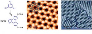
Here are images of the polymer with its chemical composition (at the left),

This image shows the polymers that were created at a resolution of 5 nanometres (the average strand of human hair is 80,000 nanometres wide) Source: Dept. of Chemistry, McGill University

I was interested to note that part of the funding for this project comes from the US Air Force since they also recently funded work on integrating memristors in electronic components (my blog posting here). Here’s my last excerpt from the news release details about the researchers’ affiliations, where the study was published, and the funding sources for the work,

Perepichka is affiliated with McGill University’s department of chemistry and Rosei is affiliated with Institut national de la recherche scientifique – Énergie Matériaux Télécommunications Center, a member of the Université du Québec network. Their research was published online by the Proceedings of the National Academy of Sciences and was funded by the Natural Sciences and Engineering Research Council of Canada, the Air Force Office of Scientific Research and Asian Office of Aerospace Research and Development of the USA, the Petroleum Research Fund of the American Chemical Society, the Fonds québécois de recherche sur la nature et les technologies, and the Ministère du Développement économique, de l’Innovation et de l’Exportation of Quebec.