EPFL researchers have developed a system that generates electricity from osmosis with unparalleled efficiency. Their work, featured in “Nature”, uses seawater, fresh water, and a new type of membrane just three atoms thick.
A July 13, 2016 news item on Nanowerk highlights research on osmotic power at École polytechnique fédérale de Lausanne (EPFL; Switzerland),
Proponents of clean energy will soon have a new source to add to their existing array of solar, wind, and hydropower: osmotic power. Or more specifically, energy generated by a natural phenomenon occurring when fresh water comes into contact with seawater through a membrane.
Researchers at EPFL’s Laboratory of Nanoscale Biology have developed an osmotic power generation system that delivers never-before-seen yields. Their innovation lies in a three atoms thick membrane used to separate the two fluids. …
The concept is fairly simple. A semipermeable membrane separates two fluids with different salt concentrations. Salt ions travel through the membrane until the salt concentrations in the two fluids reach equilibrium. That phenomenon is precisely osmosis.
If the system is used with seawater and fresh water, salt ions in the seawater pass through the membrane into the fresh water until both fluids have the same salt concentration. And since an ion is simply an atom with an electrical charge, the movement of the salt ions can be harnessed to generate electricity.
A 3 atoms thick, selective membrane that does the job
EPFL’s system consists of two liquid-filled compartments separated by a thin membrane made of molybdenum disulfide. The membrane has a tiny hole, or nanopore, through which seawater ions pass into the fresh water until the two fluids’ salt concentrations are equal. As the ions pass through the nanopore, their electrons are transferred to an electrode – which is what is used to generate an electric current.
Thanks to its properties the membrane allows positively-charged ions to pass through, while pushing away most of the negatively-charged ones. That creates voltage between the two liquids as one builds up a positive charge and the other a negative charge. This voltage is what causes the current generated by the transfer of ions to flow.
“We had to first fabricate and then investigate the optimal size of the nanopore. If it’s too big, negative ions can pass through and the resulting voltage would be too low. If it’s too small, not enough ions can pass through and the current would be too weak,” said Jiandong Feng, lead author of the research.
What sets EPFL’s system apart is its membrane. In these types of systems, the current increases with a thinner membrane. And EPFL’s membrane is just a few atoms thick. The material it is made of – molybdenum disulfide – is ideal for generating an osmotic current. “This is the first time a two-dimensional material has been used for this type of application,” said Aleksandra Radenovic, head of the laboratory of Nanoscale Biology
Powering 50’000 energy-saving light bulbs with 1m2 membrane
The potential of the new system is huge. According to their calculations, a 1m2 membrane with 30% of its surface covered by nanopores should be able to produce 1MW of electricity – or enough to power 50,000 standard energy-saving light bulbs. And since molybdenum disulfide (MoS2) is easily found in nature or can be grown by chemical vapor deposition, the system could feasibly be ramped up for large-scale power generation. The major challenge in scaling-up this process is finding out how to make relatively uniform pores.
Until now, researchers have worked on a membrane with a single nanopore, in order to understand precisely what was going on. ” From an engineering perspective, single nanopore system is ideal to further our fundamental understanding of 8=-based processes and provide useful information for industry-level commercialization”, said Jiandong Feng.
The researchers were able to run a nanotransistor from the current generated by a single nanopore and thus demonstrated a self-powered nanosystem. Low-power single-layer MoS2 transistors were fabricated in collaboration with Andras Kis’ team at at EPFL, while molecular dynamics simulations were performed by collaborators at University of Illinois at Urbana–Champaign
Harnessing the potential of estuaries
EPFL’s research is part of a growing trend. For the past several years, scientists around the world have been developing systems that leverage osmotic power to create electricity. Pilot projects have sprung up in places such as Norway, the Netherlands, Japan, and the United States to generate energy at estuaries, where rivers flow into the sea. For now, the membranes used in most systems are organic and fragile, and deliver low yields. Some systems use the movement of water, rather than ions, to power turbines that in turn produce electricity.
Once the systems become more robust, osmotic power could play a major role in the generation of renewable energy. While solar panels require adequate sunlight and wind turbines adequate wind, osmotic energy can be produced just about any time of day or night – provided there’s an estuary nearby.
Here’s a link to and a citation for the paper,
Single-layer MoS2 nanopores as nanopower generators by Jiandong Feng, Michael Graf, Ke Liu, Dmitry Ovchinnikov, Dumitru Dumcenco, Mohammad Heiranian, Vishal Nandigana, Narayana R. Aluru, Andras Kis, & Aleksandra Radenovic. Nature (2016) doi:10.1038/nature18593 Published online 13 July 2016
A June 27, 2016 news item on phys.org provides a measured analysis of deep learning and its current state of development (from a Swiss perspective),
In March 2016, the world Go champion Lee Sedol lost 1-4 against the artificial intelligence AlphaGo. For many, this was yet another defeat for humanity at the hands of the machines. Indeed, the success of the AlphaGo software was forged in an area of artificial intelligence that has seen huge progress over the last decade. Deep learning, as it’s called, uses artificial neural networks to process algorithmic calculations. This software architecture therefore mimics biological neural networks.
Much of the progress in deep learning is thanks to the work of Jürgen Schmidhuber, director of the IDSIA (Istituto Dalle Molle di Studi sull’Intelligenza Artificiale) which is located in the suburbs of Lugano. The IDSIA doctoral student Shane Legg and a group of former colleagues went on to found DeepMind, the startup acquired by Google in early 2014 for USD 500 million. The DeepMind algorithms eventually wound up in AlphaGo.
“Schmidhuber is one of the best at deep learning,” says Boi Faltings of the EPFL Artificial Intelligence Lab. “He never let go of the need to keep working at it.” According to Stéphane Marchand-Maillet of the University of Geneva computing department, “he’s been in the race since the very beginning.”
A June 27, 2016 SNSF news release (first published as a story in Horizons no. 109 June 2016) by Fabien Goubet, which originated the news item, goes on to provide a brief history,
The real strength of deep learning is structural recognition, and winning at Go is just an illustration of this, albeit a rather resounding one. Elsewhere, and for some years now, we have seen it applied to an entire spectrum of areas, such as visual and vocal recognition, online translation tools and smartphone personal assistants. One underlying principle of machine learning is that algorithms must first be trained using copious examples. Naturally, this has been helped by the deluge of user-generated content spawned by smartphones and web 2.0, stretching from Facebook photo comments to official translations published on the Internet. By feeding a machine thousands of accurately tagged images of cats, for example, it learns first to recognise those cats and later any image of a cat, including those it hasn’t been fed.
Deep learning isn’t new; it just needed modern computers to come of age. As far back as the early 1950s, biologists tried to lay out formal principles to explain the working of the brain’s cells. In 1956, the psychologist Frank Rosenblatt of the New York State Aeronautical Laboratory published a numerical model based on these concepts, thereby creating the very first artificial neural network. Once integrated into a calculator, it learned to recognise rudimentary images.
“This network only contained eight neurones organised in a single layer. It could only recognise simple characters”, says Claude Touzet of the Adaptive and Integrative Neuroscience Laboratory of Aix-Marseille University. “It wasn’t until 1985 that we saw the second generation of artificial neural networks featuring multiple layers and much greater performance”. This breakthrough was made simultaneously by three researchers: Yann LeCun in Paris, Geoffrey Hinton in Toronto and Terrence Sejnowski in Baltimore.
Byte-size learning
In multilayer networks, each layer learns to recognise the precise visual characteristics of a shape. The deeper the layer, the more abstract the characteristics. With cat photos, the first layer analyses pixel colour, and the following layer recognises the general form of the cat. This structural design can support calculations being made upon thousands of layers, and it was this aspect of the architecture that gave rise to the name ‘deep learning’.
Marchand-Maillet explains: “Each artificial neurone is assigned an input value, which it computes using a mathematical function, only firing if the output exceeds a pre-defined threshold”. In this way, it reproduces the behaviour of real neurones, which only fire and transmit information when the input signal (the potential difference across the entire neural circuit) reaches a certain level. In the artificial model, the results of a single layer are weighted, added up and then sent as the input signal to the following layer, which processes that input using different functions, and so on and so forth.
For example, if a system is trained with great quantities of photos of apples and watermelons, it will progressively learn to distinguish them on the basis of diameter, says Marchand-Maillet. If it cannot decide (e.g., when processing a picture of a tiny watermelon), the subsequent layers take over by analysing the colours or textures of the fruit in the photo, and so on. In this way, every step in the process further refines the assessment.
Video games to the rescue
For decades, the frontier of computing held back more complex applications, even at the cutting edge. Industry walked away, and deep learning only survived thanks to the video games sector, which eventually began producing graphics chips, or GPUs, with an unprecedented power at accessible prices: up to 6 teraflops (i.e., 6 trillion calculations per second) for a few hundred dollars. “There’s no doubt that it was this calculating power that laid the ground for the quantum leap in deep learning”, says Touzet. GPUs are also very good at parallel calculations, a useful function for executing the innumerable simultaneous operations required by neural networks.
Although image analysis is getting great results, things are more complicated for sequential data objects such as natural spoken language and video footage. This has formed part of Schmidhuber’s work since 1989, and his response has been to develop recurrent neural networks in which neurones communicate with each other in loops, feeding processed data back into the initial layers.
Such sequential data analysis is highly dependent on context and precursory data. In Lugano, networks have been instructed to memorise the order of a chain of events. Long Short Term Memory (LSTM) networks can distinguish ‘boat’ from ‘float’ by recalling the sound that preceded ‘oat’ (i.e., either ‘b’ or ‘fl’). “Recurrent neural networks are more powerful than other approaches such as the Hidden Markov models”, says Schmidhuber, who also notes that Google Voice integrated LSTMs in 2015. “With looped networks, the number of layers is potentially infinite”, says Faltings [?].
For Schmidhuber, deep learning is just one aspect of artificial intelligence; the real thing will lead to “the most important change in the history of our civilisation”. But Marchand-Maillet sees deep learning as “a bit of hype, leading us to believe that artificial intelligence can learn anything provided there’s data. But it’s still an open question as to whether deep learning can really be applied to every last domain”.
It’s nice to get an historical perspective and eye-opening to realize that scientists have been working on these concepts since the 1950s.
Swiss and US scientists have developed a nanoporous crystal that could be used to clean up nuclear waste gases according to a June 13, 2016 news item on Nanowerk (Note: A link has been removed),
An international team of scientists at EPFL [École polytechnique fédérale de Lausanne in Switzerland] and the US have discovered a material that can clear out radioactive waste from nuclear plants more efficiently, cheaply, and safely than current methods.
Nuclear energy is one of the cheapest alternatives to carbon-based fossil fuels. But nuclear-fuel reprocessing plants generate waste gas that is currently too expensive and dangerous to deal with. Scanning hundreds of thousands of materials, scientists led by EPFL and their US colleagues have now discovered a material that can absorb nuclear waste gases much more efficiently, cheaply and safely. The work is published in Nature Communications (“Metal–organic framework with optimally selective xenon adsorption and separation”).
Nuclear-fuel reprocessing plants generate volatile radionuclides such as xenon and krypton, which escape in the so-called “off-gas” of these facilities – the gases emitted as byproducts of the chemical process. Current ways of capturing and clearing out these gases involve distillation at very low temperatures, which is expensive in both terms of energy and capital costs, and poses a risk of explosion.
Scientists led by Berend Smit’s lab at EPFL (Sion) and colleagues in the US, have now identified a material that can be used as an efficient, cheaper, and safer alternative to separate xenon and krypton – and at room temperature. The material, abbreviated as SBMOF-1, is a nanoporous crystal and belongs a class of materials that are currently used to clear out CO2 emissions and other dangerous pollutants. These materials are also very versatile, and scientists can tweak them to self-assemble into ordered, pre-determined crystal structures. In this way, they can synthesize millions of tailor-made materials that can be optimized for gas storage separation, catalysis, chemical sensing and optics.
The scientists carried out high-throughput screening of large material databases of over 125,000 candidates. To do this, they used molecular simulations to find structures that can separate xenon and krypton, and under conditions that match those involved in reprocessing nuclear waste.
Because xenon has a much shorter half-life than krypton – a month versus a decade – the scientists had to find a material that would be selective for both but would capture them separately. As xenon is used in commercial lighting, propulsion, imaging, anesthesia and insulation, it can also be sold back into the chemical market to offset costs.
The scientists identified and confirmed that SBMOF-1 shows remarkable xenon capturing capacity and xenon/krypton selectivity under nuclear-plant conditions and at room temperature.
Researchers are investigating a new material that might help in nuclear fuel recycling and waste reduction by capturing certain gases released during reprocessing. Conventional technologies to remove these radioactive gases operate at extremely low, energy-intensive temperatures. By working at ambient temperature, the new material has the potential to save energy, make reprocessing cleaner and less expensive. The reclaimed materials can also be reused commercially.
Appearing in Nature Communications, the work is a collaboration between experimentalists and computer modelers exploring the characteristics of materials known as metal-organic frameworks.
“This is a great example of computer-inspired material discovery,” said materials scientist Praveen Thallapally of the Department of Energy’s Pacific Northwest National Laboratory. “Usually the experimental results are more realistic than computational ones. This time, the computer modeling showed us something the experiments weren’t telling us.”
Waste avoidance
Recycling nuclear fuel can reuse uranium and plutonium — the majority of the used fuel — that would otherwise be destined for waste. Researchers are exploring technologies that enable safe, efficient, and reliable recycling of nuclear fuel for use in the future.
A multi-institutional, international collaboration is studying materials to replace costly, inefficient recycling steps. One important step is collecting radioactive gases xenon and krypton, which arise during reprocessing. To capture xenon and krypton, conventional technologies use cryogenic methods in which entire gas streams are brought to a temperature far below where water freezes — such methods are energy intensive and expensive.
Thallapally, working with Maciej Haranczyk and Berend Smit of Lawrence Berkeley National Laboratory [LBNL] and others, has been studying materials called metal-organic frameworks, also known as MOFs, that could potentially trap xenon and krypton without having to use cryogenics.
These materials have tiny pores inside, so small that often only a single molecule can fit inside each pore. When one gas species has a higher affinity for the pore walls than other gas species, metal-organic frameworks can be used to separate gaseous mixtures by selectively adsorbing.
To find the best MOF for xenon and krypton separation, computational chemists led by Haranczyk and Smit screened 125,000 possible MOFs for their ability to trap the gases. Although these gases can come in radioactive varieties, they are part of a group of chemically inert elements called “noble gases.” The team used computing resources at NERSC, the National Energy Research Scientific Computing Center, a DOE Office of Science User Facility at LBNL.
“Identifying the optimal material for a given process, out of thousands of possible structures, is a challenge due to the sheer number of materials. Given that the characterization of each material can take up to a few hours of simulations, the entire screening process may fill a supercomputer for weeks,” said Haranczyk. “Instead, we developed an approach to assess the performance of materials based on their easily computable characteristics. In this case, seven different characteristics were necessary for predicting how the materials behaved, and our team’s grad student Cory Simon’s application of machine learning techniques greatly sped up the material discovery process by eliminating those that didn’t meet the criteria.”
The team’s models identified the MOF that trapped xenon most selectively and had a pore size close to the size of a xenon atom — SBMOF-1, which they then tested in the lab at PNNL.
After optimizing the preparation of SBMOF-1, Thallapally and his team at PNNL tested the material by running a mixture of gases through it — including a non-radioactive form of xenon and krypton — and measuring what came out the other end. Oxygen, helium, nitrogen, krypton, and carbon dioxide all beat xenon out. This indicated that xenon becomes trapped within SBMOF-1’s pores until the gas saturates the material.
Other tests also showed that in the absence of xenon, SBMOF-1 captures krypton. During actual separations, then, operators would pass the gas streams through SBMOF-1 twice to capture both gases.
The team also tested SBMOF-1’s ability to hang onto xenon in conditions of high humidity. Humidity interferes with cryogenics, and gases must be dehydrated before putting them through the ultra-cold method, another time-consuming expense. SBMOF-1, however, performed quite admirably, retaining more than 85 percent of the amount of xenon in high humidity as it did in dry conditions.
The final step in collecting xenon or krypton gas would be to put the MOF material under a vacuum, which sucks the gas out of the molecular cages for safe storage. A last laboratory test examined how stable the material was by repeatedly filling it up with xenon gas and then vacuuming out the xenon. After 10 cycles of this, SBMOF-1 collected just as much xenon as the first cycle, indicating a high degree of stability for long-term use.
Thallapally attributes this stability to the manner in which SBMOF-1 interacts with xenon. Rather than chemical reactions between the molecular cages and the gases, the relationship is purely physical. The material can last a lot longer without constantly going through chemical reactions, he said.
A model finding
Although the researchers showed that SBMOF-1 is a good candidate for nuclear fuel reprocessing, getting these results wasn’t smooth sailing. In the lab, the researchers had followed a previously worked out protocol from Stony Brook University to prepare SBMOF-1. Part of that protocol requires them to “activate” SBMOF-1 by heating it up to 300 degrees Celsius, three times the temperature of boiling water.
Activation cleans out material left in the pores from MOF synthesis. Laboratory tests of the activated SBMOF-1, however, showed the material didn’t behave as well as it should, based on the computer modeling results.
The researchers at PNNL repeated the lab experiments. This time, however, they activated SBMOF-1 at a lower temperature, 100 degrees Celsius, or the actual temperature of boiling water. Subjecting the material to the same lab tests, the researchers found SBMOF-1 behaving as expected, and better than at the higher activation temperature.
But why? To figure out where the discrepancy came from, the researchers modeled what happened to SBMOF-1 at 300 degrees Celsius. Unexpectedly, the pores squeezed in on themselves.
“When we heated the crystal that high, atoms within the pore tilted and partially blocked the pores,” said Thallapally. “The xenon doesn’t fit.”
Armed with these new computational and experimental insights, the researchers can explore SBMOF-1 and other MOFs further for nuclear fuel recycling. These MOFs might also be able to capture other noble gases such as radon, a gas known to pool in some basements.
Researchers hailed from several other institutions as well as those listed earlier, including University of California, Berkeley, Ecole Polytechnique Fédérale de Lausanne (EPFL) in Switzerland, Brookhaven National Laboratory, and IMDEA Materials Institute in Spain. This work was supported by the [US] Department of Energy Offices of Nuclear Energy and Science.
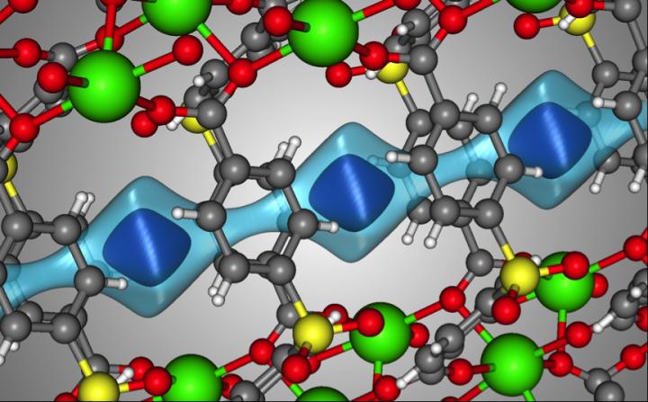
Here’s an image the researchers have provided to illustrate their work,
Caption: The crystal structure of SBMOF-1 (green = Ca, yellow = S, red = O, gray = C, white = H). The light blue surface is a visualization of the one-dimensional channel that SBMOF-1 creates for the gas molecules to move through. The darker blue surface illustrates where a Xe atom sits in the pores of SBMOF-1 when it adsorbs. Credit: Berend Smit/EPFL/University of California Berkley
Here’s a link to and a citation for the paper,
Metal–organic framework with optimally selective xenon adsorption and separation by Debasis Banerjee, Cory M. Simon, Anna M. Plonka, Radha K. Motkuri, Jian Liu, Xianyin Chen, Berend Smit, John B. Parise, Maciej Haranczyk, & Praveen K. Thallapally. Nature Communications 7, Article number: ncomms11831 doi:10.1038/ncomms11831 Published 13 June 2016
This paper is open access.
Final comment, this is the second time in the last month I’ve stumbled across more positive approaches to nuclear energy. The first time was a talk (Why Nuclear Power is Necessary) held in Vancouver, Canada in May 2016 (details here). I’m not trying to suggest anything unduly sinister but it is interesting since most of my adult life nuclear power has been viewed with fear and suspicion.
04.05.16 – Cargo ships are among the leading sources of pollution on the planet. Starting in 2020, however, stricter sulfur emission standards will take effect. A low-cost solution for reaching the new targets may come from an EPFL start-up, which is developing a nanostructured filter for use in a ship’s exhaust stacks. Copyright Alain Herzog Courtesy EPFL
A May 4, 2016 news item on Nanowerk describes a marine initiative from the École Polytechnique de Lausanne (EPFL) in Switzerland,
Around 55,000 cargo ships ply the oceans every day, powered by a fuel that is dirtier than diesel. And owing to lax standards, maritime transport has emerged as one of the leading emitters – alongside air transport – of nitrogen oxide and sulfur. But the International Maritime Organization has enacted tighter emission limits, with new standards set to take effect in 2020. In response, an EPFL start-up is developing a low-cost and eco-friendly solution: a filter that can be installed in the ships’ exhaust stacks. The start-up, Daphne Technology, could do well on this massive market.
Given that no oceans or seas border Switzerland, it’s a rather interesting initiative on their part. Here’s more from a May 4, 2015 EPFL press release, which originated the news item,
Lowering sulfur emissions to below 1%
Under laboratory conditions, the nanostructured filter is able to cut sulfur emissions to below 1% and nitrogen oxide emissions to 15% of the current standards. This is a major improvement, seeing as the new standards will require an approximately 14% reduction in sulfur emissions.
Manufacturing the filters is similar to manufacturing solar cells. A thin metal plate – titanium in this case – is nanostructured in order to increase its surface area, and a number of substances are deposited in extremely thin layers. The plates are then placed vertically and evenly spaced, creating channels through which the toxic gases travel. The gases are captured by the nanostructured surfaces. This approach is considered eco-friendly because the substances in the filter are designed to be recycled. And the exhaust gas itself becomes inert and could be used in a variety of products, such as fertilizer.
The main challenges now are to figure out a way to make these filters on large surfaces, and to bring down the cost. It was at EPFL’s Swiss Plasma Center that researcher Mario Michan found a machine that he could modify to meet his needs: it uses plasma to deposit thin layers of substances. The next step is to produce a prototype that can be tested under real-world conditions.
Michan came up with his solution for toxic gas emissions after he worked on merchant ships while completing his Master’s degree in microengineering. It took several years, some techniques he picked up in the various labs in which he worked, and a few patents for Michan to make headway on his project. It was while he was working in another field at CERN and observing the technologies used to coat the inside of particle accelerators that he discovered a process needed for his original concept. An EPFL patent tying together the various aspects of the technology and several manufacturing secrets should be filed this year.
According to the European Environment Agency, merchant ships give off 204 times more sulfur than the billion cars on the roads worldwide. Michan estimates that his nanostructured filters, if they were used by all cargo ships, would reduce these emissions to around twice the level given off by all cars, and the ships would not need to switch to another fuel. Other solutions exist, but his market research showed that they were all lacking in some way: “Marine diesel fuel is cleaner but much more expensive and would drive up fuel costs by 50% according to ship owners. And the other technologies that have been proposed cannot be used on boats or they only cut down on sulfur emissions without addressing the problem of nitrogen oxide.”
Use of nanoelectromechanical systems (NEMS) can now be maximised due to a technique developed by researchers at the Commissariat a l’Energie Atomique (CEA) and the University of Grenoble-Alpes (France). From a March 7, 2016 news item on ScienceDaily,
A joint CEA / University of Grenoble-Alpes research team, together with their international partners, have developed a diagnostic technique capable of identifying performance problems in nanoresonators, a type of nanodetector used in research and industry. These nanoelectromechanical systems, or NEMS, have never been used to their maximum capabilities. The detection limits observed in practice have always been well below the theoretical limit and, until now, this difference has remained unexplained. Using a totally new approach, the researchers have now succeeded in evaluating and explaining this phenomenon. Their results, described in the February 29 [2016] issue of Nature Nanotechnology, should now make it possible to find ways of overcoming this performance shortfall.
A Feb. 29, 2016 CEA press release, which originated the news item, provides more detail about NEMS and about the new technique,
NEMS have many applications, including the measurement of mass or force. Like a tiny violin string, a nanoresonator vibrates at a precise resonant frequency. This frequency changes if gas molecules or biological particles settle on the nanoresonator surface. This change in frequency can then be used to detect or identify the substance, enabling a medical diagnosis, for example. The extremely small dimensions of these devices (less than one millionth of a meter) make the detectors highly sensitive.
However, this resolution is constrained by a detection limit. Background noise is present in addition to the wanted measurement signal. Researchers have always considered this background noise to be an intrinsic characteristic of these systems (see Figure 2 [not reproduced here]). Despite the noise levels being significantly greater than predicted by theory, the impossibility of understanding the underlying phenomena has, until now, led the research community to ignore them.
The CEA-Leti research team and their partners reviewed all the frequency stability measurements in the literature, and identified a difference of several orders of magnitude between the accepted theoretical limits and experimental measurements.
In addition to evaluating this shortfall, the researchers also developed a diagnostic technique that could be applied to each individual nanoresonator, using their own high-purity monocrystalline silicon resonators to investigate the problem.
The resonant frequency of a nanoresonator is determined by the geometry of the resonator and the type of material used in its manufacture. It is therefore theoretically fixed. By forcing the resonator to vibrate at defined frequencies close to the resonant frequency, the CEA-Leti researchers have been able to demonstrate a secondary effect that interferes with the resolution of the system and its detection limit in addition to the background noise. This effect causes slight variations in the resonant frequency. These fluctuations in the resonant frequency result from the extreme sensitivity of these systems. While capable of detecting tiny changes in mass and force, they are also very sensitive to minute variations in temperature and the movements of molecules on their surface. At the nano scale, these parameters cannot be ignored as they impose a significant limit on the performance of nanoresonators. For example, a tiny change in temperature can change the parameters of the device material, and hence its frequency. These variations can be rapid and random.
The experimental technique developed by the team makes it possible to evaluate the loss of resolution and to determine whether it is caused by the intrinsic limits of the system or by a secondary fluctuation that can therefore by corrected. A patent has been applied for covering this technique. The research team has also shown that none of the theoretical hypotheses so far advanced to explain these fluctuations in the resonant frequency can currently explain the observed level of variation.
The research team will therefore continue experimental work to explore the physical origin of these fluctuations, with the aim of achieving a significant improvement in the performance of nanoresonators.
The Swiss Federal Institute of Technology in Lausanne, the Indian Institute of Science in Bangalore, and the California Institute of Technology (USA) have also participated in this study.The authors have received funding from the Leti Carnot Institute (NEMS-MS project) and the European Union (ERC Consolidator Grant – Enlightened project).
Here’s a link to and a citation for the paper,
Frequency fluctuations in silicon nanoresonators by Marc Sansa, Eric Sage, Elizabeth C. Bullard, Marc Gély, Thomas Alava, Eric Colinet, Akshay K. Naik, Luis Guillermo Villanueva, Laurent Duraffourg, Michael L. Roukes, Guillaume Jourdan & Sébastien Hentz. Nature Nanotechnology (2016) doi:10.1038/nnano.2016.19 Published online 29 February 2016
Perovskites, substances that perfectly absorb light, are the future of solar energy. The opportunity for their rapid dissemination has just increased thanks to a cheap and environmentally safe method of production of these materials, developed by chemists from Warsaw, Poland. Rather than in solutions at a high temperature, perovskites can now be synthesized by solid-state mechanochemical processes: by grinding powders.
We associate the milling of chemicals less often with progress than with old-fashioned pharmacies and their inherent attributes: the pestle and mortar. [emphasis mine] It’s time to change this! Recent research findings show that by the use of mechanical force, effective chemical transformations take place in solid state. Mechanochemical reactions have been under investigation for many years by the teams of Prof. Janusz Lewinski from the Institute of Physical Chemistry of the Polish Academy of Sciences (IPC PAS) and the Faculty of Chemistry of Warsaw University of Technology. In their latest publication, the Warsaw researchers describe a surprisingly simple and effective method of obtaining perovskites – futuristic photovoltaic materials with a spatially complex crystal structure.
“With the aid of mechanochemistry we are able to synthesize a variety of hybrid inorganic-organic functional materials with a potentially great significance for the energy sector. Our youngest ‘offspring’ are high quality perovskites. These compounds can be used to produce thin light-sensitive layers for high efficiency solar cells,” says Prof. Lewinski.
Perovskites are a large group of materials, characterized by a defined spatial crystalline structure. In nature, the perovskite naturally occurring as a mineral is calcium titanium(IV) oxide CaTiO3. Here the calcium atoms are arranged in the corners of the cube, in the middle of each wall there is an oxygen atom and at the centre of the cube lies a titanium atom. In other types of perovskite the same crystalline structure can be constructed of various organic and inorganic compounds, which means titanium can be replaced by, for example, lead, tin or germanium. As a result, the properties of the perovskite can be adjusted so as to best fit the specific application, for example, in photovoltaics or catalysis, but also in the construction of superconducting electromagnets, high voltage transformers, magnetic refrigerators, magnetic field sensors, or RAM memories.
At first glance, the method of production of perovskites using mechanical force, developed at the IPC PAS, looks a little like magic.
“Two powders are poured into the ball mill: a white one, methylammonium iodide CH3NH3I, and a yellow one, lead iodide PbI2. After several minutes of milling no trace is left of the substrates. Inside the mill there is only a homogeneous black powder: the perovskite CH3NH3PbI3,” explains doctoral student Anna Maria Cieslak (IPC PAS).
“Hour after hour of waiting for the reaction product? Solvents? High temperatures? In our method, all this turns out to be unnecessary! We produce chemical compounds by reactions occurring only in solids at room temperature,” stresses Dr. Daniel Prochowicz (IPC PAS).
The mechanochemically manufactured perovskites were sent to the team of Prof. Michael Graetzel from the Ecole Polytechnique de Lausanne in Switzerland, where they were used to build a new laboratory solar cell. The performance of the cell containing the perovskite with a mechanochemical pedigree proved to be more than 10% greater than a cell’s performance with the same construction, but containing an analogous perovskite obtained by the traditional method, involving solvents.
“The mechanochemical method of synthesis of perovskites is the most environmentally friendly method of producing this class of materials. Simple, efficient and fast, it is ideal for industrial applications. With full responsibility we can state: perovskites are the materials of the future, and mechanochemistry is the future of perovskites,” concludes Prof. Lewinski.
The described research will be developed within GOTSolar collaborative project funded by the European Commission under the Horizon 2020 Future and Emerging Technologies action.
Perovskites are not the only group of three-dimensional materials that has been produced mechanochemically by Prof. Lewinski’s team. In a recent publication the Warsaw researchers showed that by using the milling technique they can also synthesize inorganic-organic microporous MOF (Metal-Organic Framework) materials. The free space inside these materials is the perfect place to store different chemicals, including hydrogen.
If you want to learn how something works, one strategy is to take it apart and put it back together again [also known as reverse engineering]. For 10 years, a global initiative called the Blue Brain Project–hosted at the Ecole Polytechnique Federale de Lausanne (EPFL)–has been attempting to do this digitally with a section of juvenile rat brain. The project presents a first draft of this reconstruction, which contains over 31,000 neurons, 55 layers of cells, and 207 different neuron subtypes, on October 8 [2015] in Cell.
Heroic efforts are currently being made to define all the different types of neurons in the brain, to measure their electrical firing properties, and to map out the circuits that connect them to one another. These painstaking efforts are giving us a glimpse into the building blocks and logic of brain wiring. However, getting a full, high-resolution picture of all the features and activity of the neurons within a brain region and the circuit-level behaviors of these neurons is a major challenge.
Henry Markram and colleagues have taken an engineering approach to this question by digitally reconstructing a slice of the neocortex, an area of the brain that has benefitted from extensive characterization. Using this wealth of data, they built a virtual brain slice representing the different neuron types present in this region and the key features controlling their firing and, most notably, modeling their connectivity, including nearly 40 million synapses and 2,000 connections between each brain cell type.
“The reconstruction required an enormous number of experiments,” says Markram, of the EPFL. “It paves the way for predicting the location, numbers, and even the amount of ion currents flowing through all 40 million synapses.”
Once the reconstruction was complete, the investigators used powerful supercomputers to simulate the behavior of neurons under different conditions. Remarkably, the researchers found that, by slightly adjusting just one parameter, the level of calcium ions, they could produce broader patterns of circuit-level activity that could not be predicted based on features of the individual neurons. For instance, slow synchronous waves of neuronal activity, which have been observed in the brain during sleep, were triggered in their simulations, suggesting that neural circuits may be able to switch into different “states” that could underlie important behaviors.
“An analogy would be a computer processor that can reconfigure to focus on certain tasks,” Markram says. “The experiments suggest the existence of a spectrum of states, so this raises new types of questions, such as ‘what if you’re stuck in the wrong state?'” For instance, Markram suggests that the findings may open up new avenues for explaining how initiating the fight-or-flight response through the adrenocorticotropic hormone yields tunnel vision and aggression.
The Blue Brain Project researchers plan to continue exploring the state-dependent computational theory while improving the model they’ve built. All of the results to date are now freely available to the scientific community at https://bbp.epfl.ch/nmc-portal.
Published by the renowned journal Cell, the paper is the result of a massive effort by 82 scientists and engineers at EPFL and at institutions in Israel, Spain, Hungary, USA, China, Sweden, and the UK. It represents the culmination of 20 years of biological experimentation that generated the core dataset, and 10 years of computational science work that developed the algorithms and built the software ecosystem required to digitally reconstruct and simulate the tissue.
The Hebrew University of Jerusalem’s Prof. Idan Segev, a senior author of the research paper, said: “With the Blue Brain Project, we are creating a digital reconstruction of the brain and using supercomputer simulations of its electrical behavior to reveal a variety of brain states. This allows us to examine brain phenomena within a purely digital environment and conduct experiments previously only possible using biological tissue. The insights we gather from these experiments will help us to understand normal and abnormal brain states, and in the future may have the potential to help us develop new avenues for treating brain disorders.”
Segev, a member of the Hebrew University’s Edmond and Lily Safra Center for Brain Sciences and director of the university’s Department of Neurobiology, sees the paper as building on the pioneering work of the Spanish anatomist Ramon y Cajal from more than 100 years ago: “Ramon y Cajal began drawing every type of neuron in the brain by hand. He even drew in arrows to describe how he thought the information was flowing from one neuron to the next. Today, we are doing what Cajal would be doing with the tools of the day: building a digital representation of the neurons and synapses, and simulating the flow of information between neurons on supercomputers. Furthermore, the digitization of the tissue is open to the community and allows the data and the models to be preserved and reused for future generations.”
While a long way from digitizing the whole brain, the study demonstrates that it is feasible to digitally reconstruct and simulate brain tissue, and most importantly, to reveal novel insights into the brain’s functioning. Simulating the emergent electrical behavior of this virtual tissue on supercomputers reproduced a range of previous observations made in experiments on the brain, validating its biological accuracy and providing new insights into the functioning of the neocortex. This is a first step and a significant contribution to Europe’s Human Brain Project, which Henry Markram founded, and where EPFL is the coordinating partner.
Cell has made a video abstract available (it can be found with the Hebrew University of Jerusalem press release)
Here’s a link to and a citation for the paper,
Reconstruction and Simulation of Neocortical Microcircuitry by Henry Markram, Eilif Muller, Srikanth Ramaswamy, Michael W. Reimann, Marwan Abdellah, Carlos Aguado Sanchez, Anastasia Ailamaki, Lidia Alonso-Nanclares, Nicolas Antille, Selim Arsever, Guy Antoine Atenekeng Kahou, Thomas K. Berger, Ahmet Bilgili, Nenad Buncic, Athanassia Chalimourda, Giuseppe Chindemi, Jean-Denis Courcol, Fabien Delalondre, Vincent Delattre, Shaul Druckmann, Raphael Dumusc, James Dynes, Stefan Eilemann, Eyal Gal, Michael Emiel Gevaert, Jean-Pierre Ghobril, Albert Gidon, Joe W. Graham, Anirudh Gupta, Valentin Haenel, Etay Hay, Thomas Heinis, Juan B. Hernando, Michael Hines, Lida Kanari, Daniel Keller, John Kenyon, Georges Khazen, Yihwa Kim, James G. King, Zoltan Kisvarday, Pramod Kumbhar, Sébastien Lasserre, Jean-Vincent Le Bé, Bruno R.C. Magalhães, Angel Merchán-Pérez, Julie Meystre, Benjamin Roy Morrice, Jeffrey Muller, Alberto Muñoz-Céspedes, Shruti Muralidhar, Keerthan Muthurasa, Daniel Nachbaur, Taylor H. Newton, Max Nolte, Aleksandr Ovcharenko, Juan Palacios, Luis Pastor, Rodrigo Perin, Rajnish Ranjan, Imad Riachi, José-Rodrigo Rodríguez, Juan Luis Riquelme, Christian Rössert, Konstantinos Sfyrakis, Ying Shi, Julian C. Shillcock, Gilad Silberberg, Ricardo Silva, Farhan Tauheed, Martin Telefont, Maria Toledo-Rodriguez, Thomas Tränkler, Werner Van Geit, Jafet Villafranca Díaz, Richard Walker, Yun Wang, Stefano M. Zaninetta, Javier DeFelipe, Sean L. Hill, Idan Segev, Felix Schürmann. Cell, Volume 163, Issue 2, p456–492, 8 October 2015 DOI: http://dx.doi.org/10.1016/j.cell.2015.09.029
This paper appears to be open access.
My most substantive description of the Blue Brain Project , previous to this, was in a Jan. 29, 2013 posting featuring the European Union’s (EU) Human Brain project and involvement from countries that are not members.
* I edited a redundant lede (That’s a virtual slice of a rat brain.), moved the second sentence to the lede while adding this: *about this virtual brain slice* on Oct. 16, 2015 at 0955 hours PST.
This is for physics fans, if you plan on looking at the published paper. Otherwise, the July 20, 2015 news item on ScienceDaily is more accessible to the rest of us,
In a tremendous boost for spintronic technologies, EPFL scientists have shown that electrons can jump through spins much faster than previously thought.
Electrons spin around atoms, but also spin around themselves, and can cross over from one spin state to another. A property which can be exploited for next-generation hard drives. However, “spin cross-over” has been considered too slow to be efficient. Using ultrafast measurements, EPFL scientists have now shown for the first time that electrons can cross spins at least 100,000 times faster than previously thought. Aside for its enormous implications for fundamental physics, the finding can also propel the field of spintronics forward. …
Although difficult to describe in everyday terms, electron spin can be loosely compared to the rotation of a planet or a spinning top around its axis. Electrons can spin in different manners referred to as “spin states” and designated by the numbers 0, 1/2, 1, 3/2, 2 etc. During chemical reactions, electrons can cross from one spin state to another, e.g. from 0 to 1 or 1/2 to 3/2.
Spin cross-over is already used in many technologies, e.g. optical light-emitting devices (OLED), energy conversion systems, and cancer phototherapy. Most prominently, spin cross-over is the basis of the fledgling field of spintronics. The problem is that spin cross-over has been thought to be too slow to be efficient enough in circuits.
Spin cross-over is extremely fast
The lab of Majed Chergui at EPFL has now demonstrated that spin cross-over is considerably faster than previously thought. Using the highest time-resolution technology in the world, the lab was able to “see” electrons crossing through four spin states within 50 quadrillionths of a second — or 50 femtoseconds.
“Time resolution has always been a limitation,” says Chergui. “Over the years, labs have used techniques that could only measure spin changes to a billionth to a millionth of a second. So they thought that spin cross-over happened in this timeframe.”
Chergui’s lab focused on materials that show much promise in spintronics applications. In these materials, electrons jump through four spin-states: from 0 to 1 to 2. In 2009, Chergui’s lab pushed the boundaries of time resolution to show that this 0-2 “jump” can happen within 150 femtoseconds — suggesting that it was a direct event. Despite this, the community still maintained that such spin cross-overs go through intermediate steps.
But Chergui had his doubts. Working with his postdoc Gerald Auböck, they used the lab’s world-recognized expertise in ultrafast spectroscopy to “crank up” the time resolution. Briefly, a laser shines on the material sample under investigation, causing its electrons to move. Another laser measures their spin changes over time in the ultraviolet light range.
The finding essentially demolishes the notion of intermediate steps between spin jumps, as it does not allow enough time for them: only 50 quadrillionths of a second to go from the “0” to the “2” spin state. This is the first study to ever push time resolution to this limit in the ultraviolet domain. “This probably means that it’s even faster,” says Chergui. “But, more importantly, that it is a direct process.”
From observation to explanation
With profound implications for both technology and fundamental physics and chemistry, the study is an observation without an explanation. Chergui believes that the key is electrons shuttling back-and-forth between the iron atom at the center of the material’s molecules and its surrounding elements. “When the laser light shines on the atom, it changes the electron’s spin angle, affecting the entire spin dynamics in the molecule.”
It is now up to theoreticians to develop a new model for ultrafast spin changes. On the experimental side of things, Chergui’s lab is now focusing on actually observing electrons shuttling inside the molecules. This will require even more sophisticated approaches, such as core-level spectroscopy. Nonetheless, the study challenges ideas about spin cross-over, and might offer long-awaited solutions to the limitations of spintronics.
At this point, it’s more fitness monitor than diagnostic tool, so, you’ll still need to submit blood, stool, and urine samples when the doctor requests it but the device does offer some tantalizing possibilities according to a May 15, 2015 news item on phys.org,
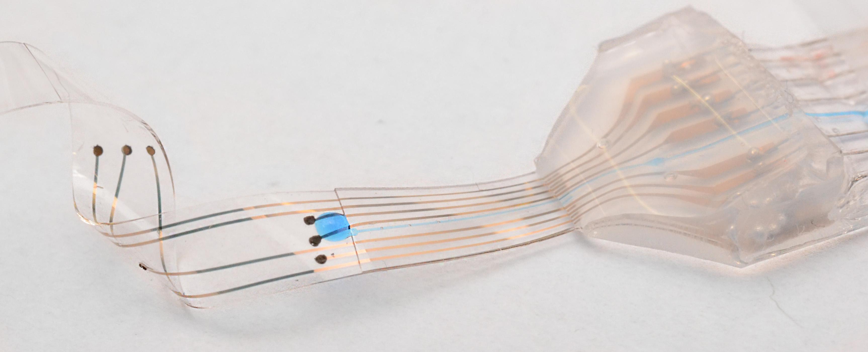
Made from state-of-the-art silicon transistors, an ultra-low power sensor enables real-time scanning of the contents of liquids such as perspiration. Compatible with advanced electronics, this technology boasts exceptional accuracy – enough to manufacture mobile sensors that monitor health.
Imagine that it is possible, through a tiny adhesive electronic stamp attached to the arm, to know in real time one’s level of hydration, stress or fatigue while jogging. A new sensor developed at the Nanoelectronic Devices Laboratory (Nanolab) at EPFL [École Polytechnique Fédérale de Lausanne in Switzerland] is the first step toward this application. “The ionic equilibrium in a person’s sweat could provide significant information on the state of his health,” says Adrian Ionescu, director of Nanolab. “Our technology detects the presence of elementary charged particles in ultra-small concentrations such as ions and protons, which reflects not only the pH balance of sweat but also more complex hydration of fatigues states. By an adapted functionalization I can also track different kinds of proteins.”
A May 15, 2015 EPFL press release by Laure-Anne Pessina, which originated the news item, includes a good technical explanation of the device for non-experts in the field,
Published in the journal ACS Nano, the device is based on transistors that are comparable to those used by the company Intel in advanced microprocessors. On the state-of-the-art “FinFET” transistor, researchers fixed a microfluidic channel through which the fluid to be analyzed flows. When the molecules pass, their electrical charge disturbs the sensor, which makes it possible to deduce the fluid’s composition.
The new device doesn’t host only sensors, but also transistors and circuits enabling the amplification of the signals – a significant innovation. The feat relies on a layered design that isolates the electronic part from the liquid substance. “Usually it is necessary to use separately a sensor for detection and a circuit for computing and signal amplification,” says Sara Rigante, lead author of the publication. “In our chip, sensors and circuits are in the same device – making it a ‘Sensing integrated circuit’. This proximity ensures that the signal is not disturbed or altered. We can thereby obtain extremely stable and accurate measurements.”
But that’s not all. Due to the size of the transistors – 20 nanometers, which is one hundred to one thousand times smaller than the thickness of a hair – it is possible to place a whole network of sensors on one chip, with each sensor locating a different particle. “We could also detect calcium, sodium or potassium in sweat,” the researcher elaborates.
As to what makes the device special (from the press release),
The technology developed at EPFL stands out from its competitors because it is extremely stable, compatible with existing electronics (CMOS), ultra-low power and easy to reproduce in large arrays of sensors. “In the field of biosensors, research around nanotechnology is intense, particularly regarding silicon nanowires and nanotubes. But these technologies are frequently unstable and therefore unusable for now in industrial applications,” says Ionescu. “In the case of our sensor, we started from extremely powerful, advanced technology and adapted it for sensing need in a liquid-gate FinFET configurations. The precision of the electronics is such that it is easy to clone our device in millions with identical characteristics.”
In addition, the technology is not energy intensive. “We could feed 10,000 sensors with a single solar cell,” Professor Ionescu asserts.
Of course, there does seem to be one shortcoming (from the press release),
Thus far, the tests have been carried out by circulating the liquid with a tiny pump. Researchers are currently working on a means of sucking the sweat into the microfluidic tube via wicking. This would rid the small analyzing “band-aid” of the need for an attached pump.
While they work on eliminating the pump part of the device, here’s a link to and a citation for the paper,
I have two items about implants and brains and an item about being able to exert remote control of the brain, all of which hint at a cyborg future for at least a few of us.
e-Dura, the spinal column, and the brain
The first item concerns some research, at the École Polytechnique de Lausanne (EPFL) which features flexible electronics. From a March 24, 2015 article by Ben Schiller for Fast Company (Note: Links have been removed),
Researchers at the Swiss Federal Institute of Technology, in Lausanne, have developed the e-Dura—a tiny skinlike device that attaches directly to damaged spinal cords. By sending out small electrical pulses, it stimulates the cord as if it were receiving signals from the brain, thus allowing movement.
“The purpose of the neuro-prosthesis is to excite the neurons that are on the spinal cord below the site of the injury and activate them, just like if they were receiving information from the brain,” says Stéphanie Lacour, a professor at the institute.
EPFL scientists have managed to get rats walking on their own again using a combination of electrical and chemical stimulation. But applying this method to humans would require multifunctional implants that could be installed for long periods of time on the spinal cord without causing any tissue damage. This is precisely what the teams of professors Stéphanie Lacour and Grégoire Courtine have developed. Their e-Dura implant is designed specifically for implantation on the surface of the brain or spinal cord. The small device closely imitates the mechanical properties of living tissue, and can simultaneously deliver electric impulses and pharmacological substances. The risks of rejection and/or damage to the spinal cord have been drastically reduced. An article about the implant will appear in early January [2015] in Science Magazine.
So-called “surface implants” have reached a roadblock; they cannot be applied long term to the spinal cord or brain, beneath the nervous system’s protective envelope, otherwise known as the “dura mater,” because when nerve tissues move or stretch, they rub against these rigid devices. After a while, this repeated friction causes inflammation, scar tissue buildup, and rejection.
Here’s what the implant looks like,
Courtesy: EPFL
The press release describes how the implant is placed (Note: A link has been removed),
Flexible and stretchy, the implant developed at EPFL is placed beneath the dura mater, directly onto the spinal cord. Its elasticity and its potential for deformation are almost identical to the living tissue surrounding it. This reduces friction and inflammation to a minimum. When implanted into rats, the e-Dura prototype caused neither damage nor rejection, even after two months. More rigid traditional implants would have caused significant nerve tissue damage during this period of time.
The researchers tested the device prototype by applying their rehabilitation protocol — which combines electrical and chemical stimulation – to paralyzed rats. Not only did the implant prove its biocompatibility, but it also did its job perfectly, allowing the rats to regain the ability to walk on their own again after a few weeks of training.
“Our e-Dura implant can remain for a long period of time on the spinal cord or the cortex, precisely because it has the same mechanical properties as the dura mater itself. This opens up new therapeutic possibilities for patients suffering from neurological trauma or disorders, particularly individuals who have become paralyzed following spinal cord injury,” explains Lacour, co-author of the paper, and holder of EPFL’s Bertarelli Chair in Neuroprosthetic Technology.
The press release goes on to describe the engineering achievements,
Developing the e-Dura implant was quite a feat of engineering. As flexible and stretchable as living tissue, it nonetheless includes electronic elements that stimulate the spinal cord at the point of injury. The silicon substrate is covered with cracked gold electric conducting tracks that can be pulled and stretched. The electrodes are made of an innovative composite of silicon and platinum microbeads. They can be deformed in any direction, while still ensuring optimal electrical conductivity. Finally, a fluidic microchannel enables the delivery of pharmacological substances – neurotransmitters in this case – that will reanimate the nerve cells beneath the injured tissue.
The implant can also be used to monitor electrical impulses from the brain in real time. When they did this, the scientists were able to extract with precision the animal’s motor intention before it was translated into movement.
“It’s the first neuronal surface implant designed from the start for long-term application. In order to build it, we had to combine expertise from a considerable number of areas,” explains Courtine, co-author and holder of EPFL’s IRP Chair in Spinal Cord Repair. “These include materials science, electronics, neuroscience, medicine, and algorithm programming. I don’t think there are many places in the world where one finds the level of interdisciplinary cooperation that exists in our Center for Neuroprosthetics.”
For the time being, the e-Dura implant has been primarily tested in cases of spinal cord injury in paralyzed rats. But the potential for applying these surface implants is huge – for example in epilepsy, Parkinson’s disease and pain management. The scientists are planning to move towards clinical trials in humans, and to develop their prototype in preparation for commercialization.
EPFL has provided a video of researcher Stéphanie Lacour describing e-Dura and expressing hopes for its commercialization,
Here’s a link to and a citation for the paper,
Electronic dura mater for long-term multimodal neural interfaces by Ivan R. Minev, Pavel Musienko, Arthur Hirsch, Quentin Barraud, Nikolaus Wenger, Eduardo Martin Moraud, Jérôme Gandar, Marco Capogrosso, Tomislav Milekovic, Léonie Asboth, Rafael Fajardo Torres, Nicolas Vachicouras, Qihan Liu, Natalia Pavlova, Simone Duis, Alexandre Larmagnac, Janos Vörös, Silvestro Micera, Zhigang Suo, Grégoire Courtine, Stéphanie P. Lacour. Science 9 January 2015: Vol. 347 no. 6218 pp. 159-163 DOI: 10.1126/science.1260318
This paper is behind a paywall.
Carbon nanotube fibres could connect to the brain
Researchers at Rice University (Texas, US) are excited about the possibilities that carbon nanotube fibres offer in the field of implantable electronics for the brain. From a March 25, 2015 news item on Nanowerk,
Carbon nanotube fibers invented at Rice University may provide the best way to communicate directly with the brain.
The fibers have proven superior to metal electrodes for deep brain stimulation and to read signals from a neuronal network. Because they provide a two-way connection, they show promise for treating patients with neurological disorders while monitoring the real-time response of neural circuits in areas that control movement, mood and bodily functions.
New experiments at Rice demonstrated the biocompatible fibers are ideal candidates for small, safe electrodes that interact with the brain’s neuronal system, according to the researchers. They could replace much larger electrodes currently used in devices for deep brain stimulation therapies in Parkinson’s disease patients.
They may also advance technologies to restore sensory or motor functions and brain-machine interfaces as well as deep brain stimulation therapies for other neurological disorders, including dystonia and depression, the researchers wrote.
The fibers created by the Rice lab of chemist and chemical engineer Matteo Pasquali consist of bundles of long nanotubes originally intended for aerospace applications where strength, weight and conductivity are paramount.
The individual nanotubes measure only a few nanometers across, but when millions are bundled in a process called wet spinning, they become thread-like fibers about a quarter the width of a human hair.
“We developed these fibers as high-strength, high-conductivity materials,” Pasquali said. “Yet, once we had them in our hand, we realized that they had an unexpected property: They are really soft, much like a thread of silk. Their unique combination of strength, conductivity and softness makes them ideal for interfacing with the electrical function of the human body.”
The simultaneous arrival in 2012 of Caleb Kemere, a Rice assistant professor who brought expertise in animal models of Parkinson’s disease, and lead author Flavia Vitale, a research scientist in Pasquali’s lab with degrees in chemical and biomedical engineering, prompted the investigation.
“The brain is basically the consistency of pudding and doesn’t interact well with stiff metal electrodes,” Kemere said. “The dream is to have electrodes with the same consistency, and that’s why we’re really excited about these flexible carbon nanotube fibers and their long-term biocompatibility.”
Weeks-long tests on cells and then in rats with Parkinson’s symptoms proved the fibers are stable and as efficient as commercial platinum electrodes at only a fraction of the size. The soft fibers caused little inflammation, which helped maintain strong electrical connections to neurons by preventing the body’s defenses from scarring and encapsulating the site of the injury.
The highly conductive carbon nanotube fibers also show much more favorable impedance – the quality of the electrical connection — than state-of-the-art metal electrodes, making for better contact at lower voltages over long periods, Kemere said.
The working end of the fiber is the exposed tip, which is about the width of a neuron. The rest is encased with a three-micron layer of a flexible, biocompatible polymer with excellent insulating properties.
The challenge is in placing the tips. “That’s really just a matter of having a brain atlas, and during the experiment adjusting the electrodes very delicately and putting them into the right place,” said Kemere, whose lab studies ways to connect signal-processing systems and the brain’s memory and cognitive centers.
Doctors who implant deep brain stimulation devices start with a recording probe able to “listen” to neurons that emit characteristic signals depending on their functions, Kemere said. Once a surgeon finds the right spot, the probe is removed and the stimulating electrode gently inserted. Rice carbon nanotube fibers that send and receive signals would simplify implantation, Vitale said.
The fibers could lead to self-regulating therapeutic devices for Parkinson’s and other patients. Current devices include an implant that sends electrical signals to the brain to calm the tremors that afflict Parkinson’s patients.
“But our technology enables the ability to record while stimulating,” Vitale said. “Current electrodes can only stimulate tissue. They’re too big to detect any spiking activity, so basically the clinical devices send continuous pulses regardless of the response of the brain.”
Kemere foresees a closed-loop system that can read neuronal signals and adapt stimulation therapy in real time. He anticipates building a device with many electrodes that can be addressed individually to gain fine control over stimulation and monitoring from a small, implantable device.
“Interestingly, conductivity is not the most important electrical property of the nanotube fibers,” Pasquali said. “These fibers are intrinsically porous and extremely stable, which are both great advantages over metal electrodes for sensing electrochemical signals and maintaining performance over long periods of time.”
The paper is open access provided you register on the website.
Remote control for stimulation of the brain
Mo Costandi, neuroscientist and freelance science writer, has written a March 24, 2015 post for the Guardian science blog network focusing on neuronal remote control,
Two teams of scientists have developed new ways of stimulating neurons with nanoparticles, allowing them to activate brain cells remotely using light or magnetic fields. The new methods are quicker and far less invasive than other hi-tech methods available, so could be more suitable for potential new treatments for human diseases.
Researchers have various methods for manipulating brain cell activity, arguably the most powerful being optogenetics, which enables them to switch specific brain cells on or off with unprecedented precision, and simultaneously record their behaviour, using pulses of light.
This is very useful for probing neural circuits and behaviour, but involves first creating genetically engineered mice with light-sensitive neurons, and then inserting the optical fibres that deliver light into the brain, so there are major technical and ethical barriers to its use in humans.
Nanomedicine could get around this. Francisco Bezanilla of the University of Chicago and his colleagues knew that gold nanoparticles can absorb light and convert it into heat, and several years ago they discovered that infrared light can make neurons fire nervous impulses by heating up their cell membranes.
…
Polina Anikeeva’s team at the Massachusetts Institute of Technology adopted a slightly different approach, using spherical iron oxide particles that give off heat when exposed to an alternating magnetic field.
…
Although still in the experimental stages, research like this may eventually allow for wireless and minimally invasive deep brain stimulation of the human brain. Bezanilla’s group aim to apply their method to develop treatments for macular degeneration and other conditions that kill off light-sensitive cells in the retina. This would involve injecting nanoparticles into the eye so that they bind to other retinal cells, allowing natural light to excite them into firing impulses to the optic nerve.
Costandi’s article is intended for an audience that either understands the science or can deal with the uncertainty of not understanding absolutely everything. Provided you fall into either of those categories, the article is well written and it provides links and citations to the papers for both research teams being featured.
Taken together, the research at EPFL, Rice University, University of Chicago, and Massachusetts Institute of Technology provides a clue as to how much money and intellectual power is being directed at the brain.