Tag Archives: germanium

Key to quantum electronics could be germanium-bonded aluminium

I have not seen aluminum called aluminium in quite some time. (I’ve always had a fondness for that extra syllable.) I first saw notice of this work from Austria in an October 11, 2021 news item on Nanowerk,

A novel electronic component from TU Wien (Vienna) could be an important key to the era of quantum information technology: Using a special manufacturing process, pure germanium is bonded with aluminium in a way that atomically sharp interfaces are created. This results in a so-called monolithic metal-semiconductor-metal heterostructure.

This structure shows unique effects that are particularly evident at low temperatures. The aluminium becomes superconducting – but not only that, this property is also transferred to the adjacent germanium semiconductor and can be specifically controlled with electric fields. This makes it excellently suited for complex applications in quantum technology, such as processing quantum bits.

A particular advantage is that using this approach, it is not necessary to develop completely new technologies. Instead, mature and well established semiconductor fabrication techniqueses can be used to enable germanium-based quantum electronics.

An October 6, 2021 Technical University of Vienna (TU Wien) press release (also on EurekAlert but published October 12, 2021), which originated the news item, delves into the technical details and the importance of temperature,

Germanium: difficult to form high-quality contacts

“Germanium is a material which will definitely play an important role in semiconductor technology for the development of faster and more energy-efficient components,” says Dr. Masiar Sistani from the Institute for Solid State Electronics at TU Wien. However, if it is used to produce components on a nanometre scale, major problems arise: the material makes it extremely difficult to produce high-quality electrical contacts. This is related to the high impact of even smallest impurities at the contact points that significantly alter the electrical properties. “We have therefore set ourselves the task of developing a new manufacturing method that enables reliable and reproducible contact properties”, says Masiar Sistani.

Diffusing atoms

The key is temperature: when nanometre-structured germanium and aluminium are brought into contact and heated, the atoms of both materials begin to diffuse into the neighbouring material – but to very different extents: the germanium atoms move rapidly into the aluminium, whereas aluminium hardly diffuses into the germanium at all. “Thus, if you connect two aluminium contacts to a thin germanium nanowire and raise the temperature to 350 degrees Celsius, the germanium atoms diffuse off the edge of the nanowire. This creates empty spaces into which the aluminium can then easily penetrate,” explains Masiar Sistani. “In the end, only a few nanometre area in the middle of the nanowire consists of germanium, the rest has been filled up by aluminium.”

Normally, aluminium is made up of tiny crystal grains, but this novel fabrication method forms a perfect single crystal in which the aluminium atoms are arranged in a uniform pattern. As can be seen under the transmission electron microscope, a perfectly clean and atomically sharp transition is formed between germanium and aluminium, with no disordered region in between. In contrast to conventional methods where electrical contacts are applied to a semiconductor, for example by evaporating a metal, no oxides can form at the boundary layer.

Quantum transport in Grenoble

In order to take a closer look at the properties of this monolithic metal-semiconductor heterostructure of germanium and aluminium at low temperature, we collaborated with Dr. Olivier Buisson and Dr. Cécile Naud from the quantum electronics circuits group at Néel Institute – CNRS-UGA [Centre National de la Recherche Scientifique; Université Grenoble Alpes] in Grenoble. It turned out that the novel structure indeed has quite remarkable properties: “Not only were we able to demonstrate superconductivity in pure, undoped germanium for the first time, we were also able to show that this structure can be switched between quite different operating states using electric fields. Such a germanium quantum dot device can not only be superconducting but also completely insulating, or it can behave like a Josephson transistor, an important basic element of quantum electronic circuits,” explains Masiar Sistani.

This new heterostructure combines a whole range of advantages: The structure has excellent physical properties needed for quantum technologies, such as high carrier mobility and excellent manipulability with electric fields, and it has the additional advantage of fitting well with already established microelectronics technologies: Germanium is already used in current chip architectures and the temperatures required for heterostructure formation are compatible with well-established semiconductor processing schemes. The novel structures not only have theoretically interesting quantum properties, but also opens up a technologically very realistic possibility of enabling further novel and energy-saving devices.

Here’s a link to and a citation for the paper,

Al–Ge–Al Nanowire Heterostructure: From Single-Hole Quantum Dot to Josephson Effect by Jovian Delaforce, Masiar Sistani, Roman B. G. Kramer, Minh A. Luong, Nicolas Roch, Walter M. Weber, Martien I. den Hertog, Eric Robin, Cecile Naud, Alois Lugstein, Olivier Buisson. Advanced Materials Volume 33, Issue 39 October 1, 2021 2101989 DOI: https://doi.org/10.1002/adma.202101989 First published [online]: 08 August 2021

This paper is behind a paywall.
Refining metals more sustainably

We don’t just extract and refine metals from the earth, increasingly, we extract and refine them from consumer goods. Researchers from McGill University (Montréal, Québec, Canada) have devised a ‘greener’ technique to do this. From a June 7, 2017 McGill University news release (received via email and also on EurekAlert),

A team of chemists in Canada has developed a way to process metals without using toxic solvents and reagents.

The system, which also consumes far less energy than conventional techniques, could greatly shrink the environmental impact of producing metals from raw materials or from post-consumer electronics.

“At a time when natural deposits of metals are on the decline, there is a great deal of interest in improving the efficiency of metal refinement and recycling, but few disruptive technologies are being put forth,” says Jean-Philip Lumb, an associate professor in McGill University’s Department of Chemistry. “That’s what makes our advance so important.”

The discovery stems from a collaboration between Lumb and Tomislav Friscic at McGill in Montreal, and Kim Baines of Western University in London, Ont. In an article published recently in Science Advances, the researchers outline an approach that uses organic molecules, instead of chlorine and hydrochloric acid, to help purify germanium, a metal used widely in electronic devices. Laboratory experiments by the researchers have shown that the same technique can be used with other metals, including zinc, copper, manganese and cobalt.

The research could mark an important milestone for the “green chemistry” movement, which seeks to replace toxic reagents used in conventional industrial manufacturing with more environmentally friendly alternatives. Most advances in this area have involved organic chemistry – the synthesis of carbon-based compounds used in pharmaceuticals and plastics, for example.

“Applications of green chemistry lag far behind in the area of metals,” Lumb says. “Yet metals are just as important for sustainability as any organic compound. For example, electronic devices require numerous metals to function.”

Taking a page from biology

There is no single ore rich in germanium, so it is generally obtained from mining operations as a minor component in a mixture with many other materials. Through a series of processes, that blend of matter can be reduced to germanium and zinc.

“Currently, in order to isolate germanium from zinc, it’s a pretty nasty process,” Baines explains. The new approach developed by the McGill and Western chemists “enables you to get germanium from zinc, without those nasty processes.”

To accomplish this, the researchers took a page from biology. Lumb’s lab for years has conducted research into the chemistry of melanin, the molecule in human tissue that gives skin and hair their color. Melanin also has the ability to bind to metals. “We asked the question: ‘Here’s this biomaterial with exquisite function, would it be possible to use it as a blueprint for new, more efficient technologies?'”

The scientists teamed up to synthesize a molecule that mimics some of the qualities of melanin. In particular, this “organic co-factor” acts as a mediator that helps to extract germanium at room temperature, without using solvents.

Next step: industrial scale

The system also taps into Friscic’s expertise in mechanochemistry, an emerging branch of chemistry that relies on mechanical force – rather than solvents and heat – to promote chemical reactions. Milling jars containing stainless-steel balls are shaken at high speeds to help purify the metal.

“This shows how collaborations naturally can lead to sustainability-oriented innovation,” Friscic says. “Combining elegant new chemistry with solvent-free mechanochemical techniques led us to a process that is cleaner by virtue of circumventing chlorine-based processing, but also eliminates the generation of toxic solvent waste”

The next step in developing the technology will be to show that it can be deployed economically on industrial scales, for a range of metals.

“There’s a tremendous amount of work that needs to be done to get from where we are now to where we need to go,” Lumb says. “But the platform works on many different kinds of metals and metal oxides, and we think that it could become a technology adopted by industry. We are looking for stakeholders with whom we can partner to move this technology forward.”

Here’s a link to and a citation for the paper,

A chlorine-free protocol for processing germanium by Martin Glavinovic, Michael Krause, Linju Yang, John A. McLeod, Lijia Liu, Kim M. Baines, Tomislav Friščić, and Jean-Philip Lumb. Science Advances 05 May 2017: Vol. 3, no. 5, e1700149 DOI: 10.1126/sciadv.1700149

This paper is open access.

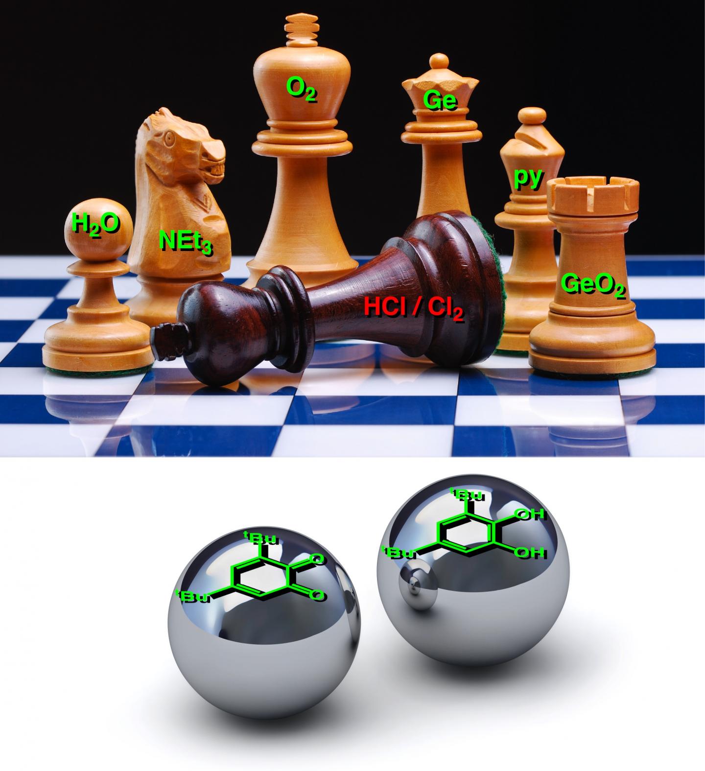
ETA June 9, 2017 at 1700 hours PDT: I have to give them marks for creativity. Here’s the image being used to illustrate the work,

Caption: Strategy for reducing the environmental impact of a refining process: replace hazardous chemicals with more benign and recyclable compounds. Credit: Michael J. Krause (Western University)

Harvard researchers look deeply into oily puddles as they rethink thin films and optical loss

For centuries it was thought that thin-film interference effects, such as those that cause oily pavements to reflect a rainbow of swirling colors, could not occur in opaque materials. Harvard physicists have now discovered that even very “lossy” thin films, if atomically thin, can be tailored to reflect a particular range of dramatic and vivid colors.

from the Oct. 14, 2012 news release on EurekAlert (also available on the Harvard School of Engineering and Applied Sciences [SEAS] news page),

The discovery is the latest to emerge from the laboratory of Federico Capasso, Robert L. Wallace Professor of Applied Physics and Vinton Hayes Senior Research Fellow in Electrical Engineering at SEAS, whose research group most recently produced ultrathin flat lenses and needle light beams that skim the surface of metals. The common thread in Capasso’s recent work is the manipulation of light at the interface of materials that are engineered at the nano- scale, a field referred to as nanophotonics. Graduate student and lead author Mikhail A. Kats carried that theme into the realm of color.

“In my group, we frequently reexamine old phenomena, where you think everything’s already known,” Capasso says. “If you have perceptive eyes, as many of my students do, you can discover exciting things that have been overlooked. In this particular case there was almost a bias among engineers that if you’re using interference, the waves have to bounce many times, so the material had better be transparent. What Mikhail’s done—and it’s admittedly simple to calculate—is to show that if you use a light-absorbing film like germanium, much thinner than the wavelength of light, then you can still see large interference effects.”

The result is a structure made of only two elements, gold and germanium (or many other possible pairings), that shines in whatever color one chooses.

These are gold films colored with nanometer-thick layers of germanium. Credit: Photo courtesy of Mikhail Kats, Romain Blanchard, and Patrice Genevet

The Oct. 14, 2012 news item on ScienceDaily notes,

“We are all familiar with the phenomenon that you see when there’s a thin film of gasoline on the road on a wet day, and you see all these different colors,” explains Capasso.

Those colors appear because the crests and troughs in the light waves interfere with each other as they pass through the oil into the water below and reflect back up into the air. Some colors (wavelengths) get a boost in brightness (amplitude), while other colors are lost.

That’s essentially the same effect that Capasso and Kats are exploiting, with coauthors Romain Blanchard and Patrice Genevet. The absorbing germanium coating traps certain colors of light while flipping the phase of others so that the crests and troughs of the waves line up closely and reflect one pure, vivid color.

“Instead of trying to minimize optical losses, we use them as an integral part of the design of thin-film coatings,” notes Kats. “In our design, reflection and absorption cooperate to give the maximum effect.”

Most astonishingly, though, a difference of only a few atoms’ thickness across the coating is sufficient to produce the dramatic color shifts. The germanium film is applied through standard manufacturing techniques — lithography and physical vapor deposition, which the researchers compare to stenciling and spray-painting — so with only a minimal amount of material (a thickness between 5 and 20 nanometers), elaborate colored designs can easily be patterned onto any surface, large or small.

“Just by changing the thickness of that film by about 15 atoms, you can change the color,” says Capasso. “It’s remarkable.”

I will never look at another oily puddle the same way again.