Tag Archives: gold

Shades of the Nokia Morph: a smartphone than conforms to your wrist

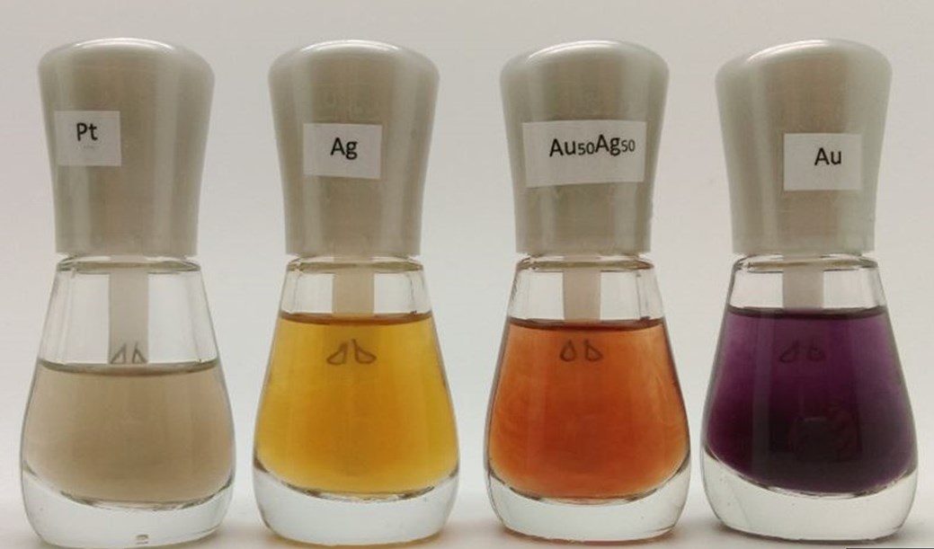
A March 16, 2017 news item on Nanowerk brought back some memories for me,

Some day, your smartphone might completely conform to your wrist, and when it does, it might be covered in pure gold, thanks to researchers at Missouri University of Science and Technology.

Nokia, a Finnish telecommunications company, was promoting its idea for a smartphone ‘and more’ that could be worn around your wrist in a concept called the Morph. It was introduced in 2008 at the Museum of Modern Art in New York City (see my March 20, 2010 posting for one of my last updates on this moribund project). Here’s Nokia’s Morph video (almost 6 mins.),

Getting back to the present day, here’s what the Missouri researchers are working on,

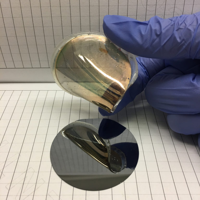
An example of a gold foil peeled from single crystal silicon. Reprinted with permission from Naveen Mahenderkar et al., Science [355]:[1203] (2017)

A March 16, 2017 Missouri University of Science and Technology news release, by Greg Katski, which originated the news item, provides more details about this Missouri version (Note: A link has been removed),

Writing in the March 17 [2017] issue of the journal Science, the S&T researchers say they have developed a way to “grow” thin layers of gold on single crystal wafers of silicon, remove the gold foils, and use them as substrates on which to grow other electronic materials. The research team’s discovery could revolutionize wearable or “flexible” technology research, greatly improving the versatility of such electronics in the future.

According to lead researcher Jay A. Switzer, the majority of research into wearable technology has been done using polymer substrates, or substrates made up of multiple crystals. “And then they put some typically organic semiconductor on there that ends up being flexible, but you lose the order that (silicon) has,” says Switzer, Donald L. Castleman/FCR Endowed Professor of Discovery in Chemistry at S&T.

Because the polymer substrates are made up of multiple crystals, they have what are called grain boundaries, says Switzer. These grain boundaries can greatly limit the performance of an electronic device.

“Say you’re making a solar cell or an LED,” he says. “In a semiconductor, you have electrons and you have holes, which are the opposite of electrons. They can combine at grain boundaries and give off heat. And then you end up losing the light that you get out of an LED, or the current or voltage that you might get out of a solar cell.”

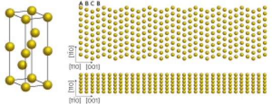
Most electronics on the market are made of silicon because it’s “relatively cheap, but also highly ordered,” Switzer says.

“99.99 percent of electronics are made out of silicon, and there’s a reason – it works great,” he says. “It’s a single crystal, and the atoms are perfectly aligned. But, when you have a single crystal like that, typically, it’s not flexible.”

By starting with single crystal silicon and growing gold foils on it, Switzer is able to keep the high order of silicon on the foil. But because the foil is gold, it’s also highly durable and flexible.

“We bent it 4,000 times, and basically the resistance didn’t change,” he says.

The gold foils are also essentially transparent because they are so thin. According to Switzer, his team has peeled foils as thin as seven nanometers.

Switzer says the challenge his research team faced was not in growing gold on the single crystal silicon, but getting it to peel off as such a thin layer of foil. Gold typically bonds very well to silicon.

“So we came up with this trick where we could photo-electrochemically oxidize the silicon,” Switzer says. “And the gold just slides off.”

Photoelectrochemical oxidation is the process by which light enables a semiconductor material, in this case silicon, to promote a catalytic oxidation reaction.

Switzer says thousands of gold foils—or foils of any number of other metals—can be made from a single crystal wafer of silicon.

The research team’s discovery can be considered a “happy accident.” Switzer says they were looking for a cheap way to make single crystals when they discovered this process.

“This is something that I think a lot of people who are interested in working with highly ordered materials like single crystals would appreciate making really easily,” he says. “Besides making flexible devices, it’s just going to open up a field for anybody who wants to work with single crystals.”

Here’s a link to and a citation for the paper,

Epitaxial lift-off of electrodeposited single-crystal gold foils for flexible electronics by Naveen K. Mahenderkar, Qingzhi Chen, Ying-Chau Liu, Alexander R. Duchild, Seth Hofheins, Eric Chason, Jay A. Switzer. Science  17 Mar 2017: Vol. 355, Issue 6330, pp. 1203-1206 DOI: 10.1126/science.aam5830

This paper is behind a paywall.

Plasmonic ‘Goldfinger’: antifungal nail polish with metallic nanoparticles

A March 29,.2017 news item on Nanowerk announces a new kind of nanopolish,

Since ancient times, people have used lustrous silver, platinum and gold to make jewelry and other adornments. Researchers have now developed a new way to add the metals to nail polish with minimal additives, resulting in durable, tinted — and potentially antibacterial — nail coloring.

Using metal nanoparticles in clear nail polish makes it durable and colorful without extra additives.
Credit: American Chemical Society

A March 29, 2017 American Chemical Society (ACS) news release (also on EurekAlert), which originated the news item, adds a little more detail (Note: A link has been removed),

Nail polish comes in a bewildering array of colors. Current coloring techniques commonly incorporate pigment powders and additives. Scientists have recently started exploring the use of nanoparticles in polishes and have found that they can improve their durability and, in the case of silver nanoparticles, can treat fungal toenail infections. Marcus Lau, Friedrich Waag and Stephan Barcikowski wanted to see if they could come up with a simple way to integrate metal nanoparticles in nail polish.

The researchers started with store-bought bottles of clear, colorless nail polish and added small pieces of silver, gold, platinum or an alloy to them. To break the metals into nanoparticles, they shone a laser on them in short bursts over 15 minutes. Analysis showed that the method resulted in a variety of colored, transparent polishes with a metallic sheen. The researchers also used laser ablation to produce a master batch of metal nanoparticles in ethyl acetate, a polish thinner, which could then be added to individual bottles of polish. This could help boost the amount of production for commercialization. The researchers say the technique could also be used to create coatings for medical devices.

The authors acknowledge funding from the INTERREG-Program Germany-Netherlands.

A transparent nail varnish can be colored simply and directly with laser-generated nanoparticles. This does not only enable coloring of the varnish for cosmetic purposes, but also gives direct access to nanodoped varnishes to be used on any solid surface. Therefore, nanoparticle properties such as plasmonic properties or antibacterial effects can be easily adapted to surfaces for medical or optical purposes. The presented method for integration of metal (gold, platinum, silver, and alloy) nanoparticles into varnishes is straightforward and gives access to nanodoped polishes with optical properties, difficult to be achieved by dispersing powder pigments in the high-viscosity liquids. Courtesy: Industrial and Engineering & Chemistry Research

Here’s a link to and a citation for the paper,

Direct Integration of Laser-Generated Nanoparticles into Transparent Nail Polish: The Plasmonic “Goldfinger” by Marcus Lau, Friedrich Waag, and Stephan Barcikowski. Ind. Eng. Chem. Res., 2017, 56 (12), pp 3291–3296 DOI: 10.1021/acs.iecr.7b00039 Publication Date (Web): March 7, 2017

Copyright © 2017 American Chemical Society

This paper is behind a paywall.

‘Golden’ protein crystals

Yet another use for gold. From a March 14, 2017 news item on Nanowerk (Note: A link has been removed),

Scientists from the London Centre for Nanotechnology (LCN) have revealed how materials such as gold can help create protein crystals. The team hope their findings, published in the journal Scientific Reports (“Protein crystal nucleation in pores”), could aid the discovery of new medicines and treatments. The Lead author; Professor Naomi Chayen states that “Gold doesn’t react with proteins, due to its inert nature, which makes it an ideal material to create crystals”.

Image: Crystals of an antibody peptide complex related to AIDS research Courtesy: LCN

A March 14, 2017 (?) LCN press release, which originated the news item, expands on the theme,

Proteins are crucial to numerous functions in the body – yet scientists are still in the dark about what most of them look like. This is because the most powerful way of revealing the structure of proteins is to turn them into crystals, and then analyse these with X-rays. However, persuading proteins to turn into useful crystals is notoriously difficult. All crystals start from a conception stage when the first molecules come together; this is called nucleation. But reaching nucleation is often difficult as it requires a lot of energy – and many proteins simply can’t overcome this barrier. Scientists also struggle to create medicines that bind to particular proteins – for instance a protein involved in cancer formation, if they don’t know the protein’s structure.

“How can you target a protein if you have no idea what it looks like? It’s like recognising a face in a crowd – you need a picture,” explained Professor Naomi Chayen, lead author of the research.

Forcing molecules together with gold

One technique for allowing proteins to reach their nucleation point is to trap them in tiny holes. This forces the molecules together, which helps them overcome the energy barrier needed to trigger the first crystal. One material that scientists have found to be effective at growing crystals is gold. Creating many holes in the metal creates a substance called porous gold, which acts as a perfect environment for growing crystals, explained Professor Chayen: “Gold doesn’t react with proteins, due to its inert nature, which makes it an ideal material to create crystals. Creating holes in the metal enable it to act a bit like coral, with each hole providing an ideal environment to harbour crystals.”

Creating crystals

In the latest research, the team investigated the best size hole needed to create crystals. They found that a variety of different sized holes produced the highest quality crystals. Most holes were around 5-10nm, just slightly larger than the width of a human hair. Professor Chayen explained: “Imagine walking down a street with many potholes – some of the holes will be big enough for me to step out of, while some will be too small for my foot to fall into. “However, some will be the exact size of my foot, and will trap me in them. This is the same principle as having different pore sizes – it allows us to trap different size protein molecules, enabling them to form crystals.”

She added that the findings which give a simple explanation of why, and under what conditions porous materials can induce protein crystal nucleation may help scientists design porous materials that would produce the highest quality crystals.

Here’s a link to and a citation for the paper,

Protein crystal nucleation in pores by Christo N. Nanev, Emmanuel Saridakis & Naomi E. Chayen. Scientific Reports 7, Article number: 35821 (2017) doi:10.1038/srep35821 Published online: 16 January 2017

This is an open access article.

Pure gold nanostructures

This Nov. 4, 2016 news item on ScienceDaily features another ‘alchemy’ story although this one is truer to the source material than some of the other stories,

The idea is reminiscent of the ancient alchemists’ attempts to create gold from worthless substances: Researchers have discovered a novel way to fabricate pure gold nanostructures using an additive direct-write lithography technique. An electron beam is used to turn an auriferous organic compound into pure gold. This new technique can now be used to create nanostructures, which are needed for many applications in electronics and sensor technology. Just like with a 3D-printer on the nanoscale, almost any arbitrary shape can be created.

Caption: Nanostructure made of gold. Credit: TU Wien

Caption: Nanostructure made of gold. Credit: TU Wien

A Nov. 3, 2016 Technical University of Vienna (Technische Universität Wien) press release (also so on EurekAlert), which originated the news item, expands on the theme,

“Gold is not only a noble metal of exceptional beauty, but also a highly desired material for functional nanostructures”, says Professor Heinz Wanzenböck from TU Wien. Especially patterned gold nanostructures are key enabling structures in plasmonic devices, for biosensors with immobilized antibodies and as electrical contacts. For decades the fabrication of pure gold nanostructures on non-planar surfaces as well as of 3-dimensional gold nanostructures has been the bottleneck. Up to now, only 2-dimensional gold nanostructures on planar surfaces were achievable by resist based lithography.

The new technology, developed at TU Wien, can now solve this problem. The principle is the local decomposition of a metalorganic precursor by the focused electron beam of an electron microscope. With extremely high precision, the electron beam can decompose the organic compound at exactly the right position, leaving behind a 3D-trail of solid gold.

The final obstacle was getting the material purity right, as the electron-induced decomposition of metalorganic precursors has typically yielded metals with high carbon contaminations. This last bottleneck on the road to custom-designed, pure gold nanostructures has now been overcome as described in the work on “Highly conductive and pure gold nanostructures grown by electron beam induced deposition” published in Scientific Reports.

While conventional gold deposition usually contains about 70 atomic % carbon and only 30 atomic % gold, the new approach developed by a research group lead by Dr. Heinz Wanzenboeck at TU Wien has allowed to fabricate pure gold structures by in-situ addition of an oxidizing agent during the gold deposition. “The whole community has been working hard for the last 10 years to directly deposit pure gold nanostructures”, says Heinz Wanzenböck. At last, the group’s expertise in engineering and chemical reactions paid off and direct deposition of pure gold was successful. “It’s a bit like discovering the legendary philosopher’s stone that turns common, ignoble material into gold” joked Wanzenboeck.

This deposited pure gold structure exhibits extremely low resistivity near that of bulk gold. Generally, a FEBID gold structure has a resistivity around 1-Ohm-cm which is about 1 million times worse than the resistivity of purest bulk gold. However, this specially enhanced FEBID process produces a resistivity of 8.8 micro-Ohm-cm which is only a factor 4 away from the bulk resistivity of purest gold (2.4 micro-Ohm-cm).

The authors of the paper Dr. Mostafa Moonir Shawrav and Dipl.Ing. Philipp Taus stated, “This highly conductive and pure gold structure will open a new door for novel nanoelectronic devices. For example, it will be easier to produce pure gold structures for nanoantennas and biomolecule immobilization which will change our everyday life”. Dr. Shawrav added “it is remarkable how a regular SEM (Scanning Electron Microscope) nowadays can deposit nanostructures compared to 20 years back when it was only a characterization device”. And with pure gold direct deposition available now, he expects nanodevices to be deposited directly and utilized in many different applications for technological revolution. Concluding, this work is a giant leap forward for 3D nano-printing of gold structures which will be the core part of nanoplasmonics and bioelectronics devices.

Here’s  a link to and a citation for the paper,

Highly conductive and pure gold nanostructures grown by electron beam induced deposition by Mostafa M. Shawrav, Philipp Taus, Heinz D. Wanzenboeck, M. Schinnerl, M. Stöger-Pollach, S. Schwarz, A. Steiger-Thirsfeld, & Emmerich Bertagnolli. Scientific Reports 6, Article number: 34003 (2016)  doi:10.1038/srep34003 Published online: 26 September 2016

This paper is open access.

Producing catalytically active gold nanoparticles at absolute zero

A Sept. 8, 2016 news item on Nanowerk describes research into producing remarkably stable gold nanoparticles with catalytic capabilities (Note: A link has been removed),

An ultra-high-vacuum chamber with temperatures approaching absolute zero—the coldest anything can get—may be the last place you would expect to find gold. But a group of researchers from Stony Brook University (SBU) in collaboration with scientists at the Air Force Research Lab (AFRL) and the U.S. Department of Energy’s (DOE) Brookhaven National Laboratory have just demonstrated that such a desolate place is ideal for producing catalytically active gold nanoparticles.

A paper describing the first catalyst ever produced using their new method, called Helium Nanodroplet Deposition (HND), was recently published in the Journal of Physical Chemistry Letters (“Development of a New Generation of Stable, Tunable, and Catalytically Active Nanoparticles Produced by the Helium Nanodroplet Deposition Method”).

A Sept. 7, 2016 Brookhaven National Laboratory news release by Alexander Orlov and Karen McNulty Walsh, which originated the news item, describes the work in more detail,

As lead researcher Alexander Orlov of SBU explains, HND works by boiling gold atoms in a vacuum to produce a vapor. The vaporized gold is then “picked up” by an extremely cold jet stream of liquid helium droplets that act to literally strike gold clusters against a solid collector downstream. Upon striking the collector, the liquid helium droplets instantly evaporate releasing helium gas and leaving behind unprecedentedly pure and stable gold nanoparticles.

“This new method to produce active nanoparticles offers unique opportunities to create materials with unprecedented properties to solve energy and environmental problems,” Orlov said.  “Our Brookhaven and AFRL collaborators made it possible for our students to access the most unique facilities in the world, which made all the difference in our research.”

Qiyuan Wu, a graduate student working in Orlov’s laboratory and first author on the paper, performed much of the work to develop the method. Michael Lindsay and Claron Ridge of AFRL provided state-of-the-art facilities at Eglin Air Force Base, one of only a few places in the world with the capabilities required to generate the gold nanoparticles using the new technique. And a team at the Center for Functional Nanomaterials (CFN), a DOE Office of Science User Facility at Brookhaven Lab, used advanced imaging and characterization tools to study the nanoparticles’ catalytic activity.

Specifically, Brookhaven scientists Eric Stach and Dmitri Zakharov of the CFN and Shen Zhao, then a postdoctoral fellow working under Stach, developed a method to deposit the gold nanoparticles onto a “catalyst support” structure they use for characterizing the stability of other nanomaterials. They then studied the characteristics of the nanoparticles, including their stability under reaction conditions, using the Titan Environmental Transmission Electron Microscope at the CFN. Further characterization by Zhao and CFN staff member Dong Su using aberration-corrected Scanning Transmission Electron Microscopy allowed the SBU researchers to understand how the droplets form.

“This was part of a User project, that morphed into a collaboration,” said Stach, who leads the electron microscopy group at CFN. “It was a very nice study”—and an example of how the Office of Science User Facilities offer not just unique scientific equipment but also scientific expertise that can be essential to the success of a research project.

Nanoparticles are of high research interest due to their improved properties compared to bulk materials. They have revolutionized technologies aimed at improving sustainability such as fuel cells, photocatalysts, and solar panels. The gold nanoparticle catalysts produced in this study are capable of converting poisonous carbon monoxide gas into carbon dioxide gas, an essential reaction that occurs in the catalytic converters of cars to reduce pollution and lower impacts on the environment.

According to Orlov, the HND method is not limited to the production of gold nanoparticles, but can be applied to nearly all metals and can even produce challenging multi-metallic nanoparticles. The technique’s versatility and ability to produce clean and well-defined samples make it a powerful tool for the discovery of new catalysts and studying factors that affect catalyst performance.

The collaboration is currently researching how the parameters of HND can be adjusted to control catalyst performance.

Here’s a link to and a citation for the paper,

Development of a New Generation of Stable, Tunable, and Catalytically Active Nanoparticles Produced by the Helium Nanodroplet Deposition Method by Qiyuan Wu, Claron J. Ridge, Shen Zhao, Dmitri Zakharov, Jiajie Cen, Xiao Tong, Eoghan Connors, Dong Su, Eric A. Stach, C. Michael Lindsay, and Alexander Orlov. J. Phys. Chem. Lett., 2016, 7 (15), pp 2910–2914 DOI: 10.1021/acs.jpclett.6b01305 Publication Date (Web): July 13, 2016

Copyright © 2016 American Chemical Society

This paper is behind a paywall.

Ultimate discovery tool?

For anyone familiar with the US nanomedicine scene, Chad Mirkin’s appearance in this announcement from Northwestern University isn’t much of a surprise.  From a June 23, 2016 news item on ScienceDaily,

The discovery power of the gene chip is coming to nanotechnology. A Northwestern University research team is developing a tool to rapidly test millions and perhaps even billions or more different nanoparticles at one time to zero in on the best particle for a specific use.

When materials are miniaturized, their properties—optical, structural, electrical, mechanical and chemical—change, offering new possibilities. But determining what nanoparticle size and composition are best for a given application, such as catalysts, biodiagnostic labels, pharmaceuticals and electronic devices, is a daunting task.

“As scientists, we’ve only just begun to investigate what materials can be made on the nanoscale,” said Northwestern’s Chad A. Mirkin, a world leader in nanotechnology research and its application, who led the study. “Screening a million potentially useful nanoparticles, for example, could take several lifetimes. Once optimized, our tool will enable researchers to pick the winner much faster than conventional methods. We have the ultimate discovery tool.”

A June 23, 2016 Northwestern University news release (also on EurekAlert), which originated the news item, describes the work in more detail,

Using a Northwestern technique that deposits materials on a surface, Mirkin and his team figured out how to make combinatorial libraries of nanoparticles in a very controlled way. (A combinatorial library is a collection of systematically varied structures encoded at specific sites on a surface.) Their study will be published June 24 by the journal Science.

The nanoparticle libraries are much like a gene chip, Mirkin says, where thousands of different spots of DNA are used to identify the presence of a disease or toxin. Thousands of reactions can be done simultaneously, providing results in just a few hours. Similarly, Mirkin and his team’s libraries will enable scientists to rapidly make and screen millions to billions of nanoparticles of different compositions and sizes for desirable physical and chemical properties.

“The ability to make libraries of nanoparticles will open a new field of nanocombinatorics, where size — on a scale that matters — and composition become tunable parameters,” Mirkin said. “This is a powerful approach to discovery science.”

“I liken our combinatorial nanopatterning approach to providing a broad palette of bold colors to an artist who previously had been working with a handful of dull and pale black, white and grey pastels,” said co-author Vinayak P. Dravid, the Abraham Harris Professor of Materials Science and Engineering in the McCormick School of Engineering.

Using five metallic elements — gold, silver, cobalt, copper and nickel — Mirkin and his team developed an array of unique structures by varying every elemental combination. In previous work, the researchers had shown that particle diameter also can be varied deliberately on the 1- to 100-nanometer length scale.

Some of the compositions can be found in nature, but more than half of them have never existed before on Earth. And when pictured using high-powered imaging techniques, the nanoparticles appear like an array of colorful Easter eggs, each compositional element contributing to the palette.

To build the combinatorial libraries, Mirkin and his team used Dip-Pen Nanolithography, a technique developed at Northwestern in 1999, to deposit onto a surface individual polymer “dots,” each loaded with different metal salts of interest. The researchers then heated the polymer dots, reducing the salts to metal atoms and forming a single nanoparticle. The size of the polymer dot can be varied to change the size of the final nanoparticle.

This control of both size and composition of nanoparticles is very important, Mirkin stressed. Having demonstrated control, the researchers used the tool to systematically generate a library of 31 nanostructures using the five different metals.

To help analyze the complex elemental compositions and size/shape of the nanoparticles down to the sub-nanometer scale, the team turned to Dravid, Mirkin’s longtime friend and collaborator. Dravid, founding director of Northwestern’s NUANCE Center, contributed his expertise and the advanced electron microscopes of NUANCE to spatially map the compositional trajectories of the combinatorial nanoparticles.

Now, scientists can begin to study these nanoparticles as well as build other useful combinatorial libraries consisting of billions of structures that subtly differ in size and composition. These structures may become the next materials that power fuel cells, efficiently harvest solar energy and convert it into useful fuels, and catalyze reactions that take low-value feedstocks from the petroleum industry and turn them into high-value products useful in the chemical and pharmaceutical industries.

Here’s a diagram illustrating the work,

 Caption: A combinatorial library of polyelemental nanoparticles was developed using Dip-Pen Nanolithography. This novel nanoparticle library opens up a new field of nanocombinatorics for rapid screening of nanomaterials for a multitude of properties. Credit: Peng-Cheng Chen/James Hedrick

Caption: A combinatorial library of polyelemental nanoparticles was developed using Dip-Pen Nanolithography. This novel nanoparticle library opens up a new field of nanocombinatorics for rapid screening of nanomaterials for a multitude of properties. Credit: Peng-Cheng Chen/James Hedrick

Here’s a link to and a citation for the paper,

Polyelemental nanoparticle libraries by Peng-Cheng Chen, Xiaolong Liu, James L. Hedrick, Zhuang Xie, Shunzhi Wang, Qing-Yuan Lin, Mark C. Hersam, Vinayak P. Dravid, Chad A. Mirkin. Science  24 Jun 2016: Vol. 352, Issue 6293, pp. 1565-1569 DOI: 10.1126/science.aaf8402

This paper is behind a paywall.

The origins of gold and other precious metals

The link between this research and my side project on gold nanoparticles is a bit tenuous but this work on the origins for gold and other precious metals being found in the stars is so fascinating and I’m determined to find a connection.

An artist's impression of two neutron stars colliding. (Credit: Dana Berry / Skyworks Digital, Inc.) Courtesy: Kavli Foundation

An artist’s impression of two neutron stars colliding. (Credit: Dana Berry / Skyworks Digital, Inc.) Courtesy: Kavli Foundation

From a May 19, 2016 news item on phys.org,

The origin of many of the most precious elements on the periodic table, such as gold, silver and platinum, has perplexed scientists for more than six decades. Now a recent study has an answer, evocatively conveyed in the faint starlight from a distant dwarf galaxy.

In a roundtable discussion, published today [May 19, 2016?], The Kavli Foundation spoke to two of the researchers behind the discovery about why the source of these heavy elements, collectively called “r-process” elements, has been so hard to crack.

From the Spring 2016 Kavli Foundation webpage hosting the  “Galactic ‘Gold Mine’ Explains the Origin of Nature’s Heaviest Elements” Roundtable ,

RESEARCHERS HAVE SOLVED a 60-year-old mystery regarding the origin of the heaviest elements in nature, conveyed in the faint starlight from a distant dwarf galaxy.

Most of the chemical elements, composing everything from planets to paramecia, are forged by the nuclear furnaces in stars like the Sun. But the cosmic wellspring for a certain set of heavy, often valuable elements like gold, silver, lead and uranium, has long evaded scientists.

Astronomers studying a galaxy called Reticulum II have just discovered that its stars contain whopping amounts of these metals—collectively known as “r-process” elements (See “What is the R-Process?”). Of the 10 dwarf galaxies that have been similarly studied so far, only Reticulum II bears such strong chemical signatures. The finding suggests some unusual event took place billions of years ago that created ample amounts of heavy elements and then strew them throughout the galaxy’s reservoir of gas and dust. This r-process-enriched material then went on to form Reticulum II’s standout stars.

Based on the new study, from a team of researchers at the Kavli Institute at the Massachusetts Institute of Technology, the unusual event in Reticulum II was likely the collision of two, ultra-dense objects called neutron stars. Scientists have hypothesized for decades that these collisions could serve as a primary source for r-process elements, yet the idea had lacked solid observational evidence. Now armed with this information, scientists can further hope to retrace the histories of galaxies based on the contents of their stars, in effect conducting “stellar archeology.”

The Kavli Foundation recently spoke with three astrophysicists about how this discovery can unlock clues about galactic evolution as well as the abundances of certain elements on Earth we use for everything from jewelry-making to nuclear power generation. The participants were:

  • Alexander Ji – is a graduate student in physics at the Massachusetts Institute of Technology (MIT) and a member of the MIT Kavli Institute for Astrophysics and Space Research (MKI). He is lead author of a paper in Nature describing this discovery.
  • Anna Frebel – is the Silverman Family Career Development Assistant Professor in the Department of Physics at MIT and also a member of MKI. Frebel is Ji’s advisor and coauthored the Nature paper. Her work delves into the chemical and physical conditions of the early universe as conveyed by the oldest stars.
  • Enrico Ramirez-Ruiz – is a Professor of Astronomy and Astrophysics at the University of California, Santa Cruz. His research explores violent events in the universe, including the mergers of neutron stars and their role in generating r-process elements.

Here’s a link to and citation for Ji’s and Frebel’s paper about r-process elements in the stars,

R-process enrichment from a single event in an ancient dwarf galaxy by Alexander P. Ji, Anna Frebel, Anirudh Chiti, & Joshua D. Simon. Nature 531, 610–613 (31 March 2016) doi:10.1038/nature17425 Published online 21 March 2016

This paper is behind a paywall but you can read an edited transcript of the roundtable discussion on the Galactic ‘Gold Mine’ Explains the Origin of Nature’s Heaviest Elements webpage (keep scrolling past the introductory text).

As for my side project, Steep (2) on gold nanoparticles, that’s still in the planning stages but if there’s a way to include this information, I’ll do it.

Gold nanoparticles and two different collective oscillations

An April 27, 2016 news item on phys.org describes research into gold nanoparticles and Surface Plasmon Resonance at Hokkaido University and the University of Tsukuba (Japan),

The research group of Professor Hiroaki Misawa of Research Institute for Electronic Science, Hokkaido University and Assistant Professor Atsushi Kubo of the Faculty of Pure and Applied Sciences, University of Tsukuba, have successfully observed the dephasing time of the two different types of collective motions of electrons generated on the surface of a gold nanoparticle for the first time in the world, by combining a laser that emits ultrashort light pulses with a photoemission electron microscope.

An April 26, 2016 Hokkaido University press release, which originated the news item, explains further,

When gold is reduced to the size in nanometer scale, its color is red instead of gold. When gold nanoparticles are exposed to light, the collective oscillations of electrons existing on the localized surface of the gold causes red light to be strongly absorbed and dispersed.

This phenomenon is called Surface Plasmon Resonance. The red color of stained glass is also a result of this phenomenon. Recently, gold nanoparticles have been widely used in various fields, such as application in pregnancy tests.

This collective oscillations of electrons on the surface of gold nanoparticles caused by light was considered to be a phenomenon that sustained only for an extremely short time, and difficult to measure due to this shortness.

Our research group developed a methodology to measure the dephasing time of the collective oscillations of electrons occurring on the surface of gold nanoparticles by combining a laser that emits ultrashort light pulses of a few femtoseconds (1 femtosecond: 1´10-15 seconds), and a photoemission electron microscope in high spatial resolution.

When measured by this technique, the different dephasing times of the two different collective oscillations, namely dipole and quadrupole surface plasmon modes, could be resolved and identified as 5 femtoseconds and 9 femtoseconds, respectively.

Research using gold nanoparticles as optical antennae to harvest light for photovoltaic cell and an artificial photosynthesis system that can split water to obtain hydrogen is progressing. The successful measurement of the dephasing time of the collective oscillations of electrons is considered to be a useful guideline in developing these systems.

Here’s a link to and a citation for the paper,

Dissecting the Few-Femtosecond Dephasing Time of Dipole and Quadrupole Modes in Gold Nanoparticles Using Polarized Photoemission Electron Microscopy by Quan Sun†, Han Yu, Kosei Ueno, Atsushi Kubo, Yasutaka Matsuo, and Hiroaki Misawa. ACS Nano, 2016, 10 (3), pp 3835–3842 DOI: 10.1021/acsnano.6b00715Publication Date (Web): February 15, 2016

Copyright © 2016 American Chemical Society

This paper appears to be open access.

South Africa, energy, and nanotechnology

South African academics Nosipho Moloto, Associate Professor, Department of Chemistry, University of the Witwatersrand and Siyabonga P. Ngubane, Lecturer in Chemistry, University of the Witwatersrand have written a Feb. 17, 2016 article for The Conversation (also available on the South African Broadcasting Corporation website) about South Africa’s energy needs and its nanotechnology efforts (Note: Links have been removed),

Energy is an economic driver of both developed and developing countries. South Africa over the past few years has faced an energy crisis with rolling blackouts between 2008 and 2015. Part of the problem has been attributed to mismanagement by the state-owned utility company Eskom, particularly the shortcomings of maintenance plans on several plants.

But South Africa has two things going for it that could help it out of its current crisis. By developing a strong nanotechnology capability and applying this to its rich mineral reserves the country is well-placed to develop new energy technologies.

Nanotechnology has already shown that it has the potential to alleviate energy problems. …

It can also yield materials with new properties and the miniaturisation of devices. For example, since the discovery of graphene, a single atomic layer of graphite, several applications in biological engineering, electronics and composite materials have been identified. These include economic and efficient devices like solar cells and lithium ion secondary batteries.

Nanotechnology has seen an incredible increase in commercialisation. Nearly 10,000 patents have been filed by large corporations since its beginning in 1991. There are already a number of nanotechnology products and solutions on the market. Examples include Miller’s beer bottling composites, Armor’s N-Force line bulletproof vests and printed solar cells produced by Nanosolar – as well as Samsung’s nanotechnology television.

The advent of nanotechnology in South Africa began with the South African Nanotechnology Initiative in 2002. This was followed by the a [sic] national nanotechnology strategy in 2003.

The government has spent more than R450 million [Rand] in nanotechnology and nanosciences research since 2006. For example, two national innovation centres have been set up and funding has been made available for equipment. There has also been flagship funding.

The country could be globally competitive in this field due to the infancy of the technology. As such, there are plenty of opportunities to make novel discoveries in South Africa.

Mineral wealth

There is another major advantage South Africa has that could help diversify its energy supply. It has an abundance of mineral wealth with an estimated value of US$2.5 trillion. The country has the world’s largest reserves of manganese and platinum group metals. It also has massive reserves of gold, diamonds, chromite ore and vanadium.

Through beneficiation and nanotechnology these resources could be used to cater for the development of new energy technologies. Research in beneficiation of minerals for energy applications is gaining momentum. For example, Anglo American and the Department of Science and Technology have embarked on a partnership to convert hydrogen into electricity.

The Council for Scientific and Industrial research also aims to develop low cost lithium ion batteries and supercapacitors using locally mined manganese and titanium ores. There is collaborative researchto use minerals like gold to synthesize nanomaterials for application in photovoltaics.

The current photovoltaic market relies on importing solar cells or panels from Europe, Asia and the US for local assembly to produce arrays. South African UV index is one of the highest in the world which reduces the lifespan of solar panels. The key to a thriving and profitable photovoltaic sector therefore lies in local production and research and development to support the sector.

It’s worth reading the article in its entirety if you’re interested in a perspective on South Africa’s energy and nanotechnology efforts.

Not the same old gold: there’s a brand new phase

A Dec. 7, 2015 news item on ScienceDaily announces a new phase for gold has been identified,

A new and stable phase of gold with different physical and optical properties from those of conventional gold has been synthesized by Agency for Science, Technology and Research (A*STAR) researchers [1], Singapore, and promises to be useful for a wide range of applications, including plasmonics and catalysis.

Many materials exist in a variety of crystal structures, known as phases or polymorphs. These different phases have the same chemical composition but different physical structures, which give rise to different properties. For example, two well-known polymorphs of carbon, graphite and diamond, arranged differently, have radically different physical properties, despite being the same element.

Gold has been used for many purposes throughout history, including jewelry, electronics and catalysis. Until now it has always been produced in one phase ― a face-centered cubic structure in which atoms are located at the corners and the center of each face of the constituent cubes.

Now, Lin Wu and colleagues at the Institute of the A*STAR Institute of High Performance Computing have modeled the optical and plasmonic properties of nanoscale ribbons of a new phase of gold — the 4H hexagonal phase (…) — produced and characterized by collaborators at other institutes in Singapore, China and the USA. The team synthesized nanoribbons of the new phase by simply heating the gold (III) chloride hydrate (HAuCl4) with a mixture of three organic solvents and then centrifuging and washing the product. This gave a high yield of about 60 per cent.

Here’s an image supplied by the researchers,

The atomic structure of the new phase of gold synthesized by A*STAR researchers. Reproduced from Ref. 1 and licensed under CC BY 4.0 © 2015 Z. Fan et al.

The atomic structure of the new phase of gold synthesized by A*STAR researchers. Reproduced from Ref. 1 and licensed under CC BY 4.0 © 2015 Z. Fan et al.

A Dec. 2, 2015 A*STAR news release, which originated the news item, provides more details,

The researchers also produced 4H hexagonal phases of the precious metals silver, platinum and palladium by growing them on top of the gold 4H hexagonal phase.

The cubic phase looks identical when viewed front on, from one side or from above. In contrast, the new 4H hexagonal phase lacks this cubic symmetry and hence varies more with direction — a property known as anisotropy. This lower symmetry gives it more directionally varying optical properties, which may make it useful for plasmonic applications. “Our finding is not only is of fundamental interest, but it also provides a new avenue for unconventional applications of plasmonic devices,” says Wu.

The team is keen to explore the potential of their new phase. “In the future, we hope to leverage the unconventional anisotropic properties of the new gold phase and design new devices with excellent performances not achievable with conventional face-centered-cubic gold,” says Wu. The synthesis method also gives rise to the potential for new strategies for controlling the crystalline phase of nanomaterials made from the noble metals.

Here’s a link to and a citation for the paper,

Stabilization of 4H hexagonal phase in gold nanoribbons by Zhanxi Fan, Michel Bosman, Xiao Huang, Ding Huang, Yi Yu, Khuong P. Ong, Yuriy A. Akimov, Lin Wu, Bing Li, Jumiati Wu, Ying Huang, Qing Liu, Ching Eng Png, Chee Lip Gan, Peidong Yang & Hua Zhang. Nature Communications 6, Article number: 7684 doi:10.1038/ncomms8684 Published 28 July 2015

This is an open access paper.