Tag Archives: gold nanocrystals

Graphene liquid cells and movies at the nanoscale

Here’s an Oct. 3, 2013 news item on Azonano about transmission electron microscopy (TEM) and graphene liquid cells enabling researchers at the Lawrence Berkeley National Laboratory (Berkeley Lab) to make movies,

Through a combination of transmission electron microscopy (TEM) and their own unique graphene liquid cell, the researchers have recorded the three-dimensional motion of DNA connected to gold nanocrystals. This is the first time TEM has been used for 3D dynamic imaging of so-called soft materials.

The researchers have produced an animation illustrating their work,

The Oct. 3, 2013 Berkeley Lab news release, which originated the news item, goes on to describe the challenge of imaging soft materials and how the researchers solved the problem,

In the past, liquid cells featured silicon-based viewing windows whose thickness limited resolution and perturbed the natural state of the soft materials. Zettl [physicist Alex Zettl] and Alivisatos [Paul Alivisatos, Berkeley Lab Director] and their respective research groups overcame these limitations with the development of a liquid cell based on a graphene membrane only a single atom thick. This development was done in close cooperation with researchers at the National Center for Electron Microscopy (NCEM), which is located at Berkeley Lab.

“Our graphene liquid cells pushed the spatial resolution of liquid phase TEM imaging to the atomic scale but still focused on growth trajectories of metallic nanocrystals,” says lead author Qian Chen, a postdoctoral fellow in Alivisatos’s research group. “Now we’ve adopted the technique to imaging the 3D dynamics of soft materials, starting with double-strand (dsDNA) connected to gold nanocrystals and achieved nanometer resolution.”

To create the cell, two opposing graphene sheets are bonded to one another by their van der Waals attraction. This forms a sealed nanoscale chamber and creates within the chamber a stable aqueous solution pocket approximately 100 nanometers in height and one micron in diameter. The single atom thick graphene membrane of the cells is essentially transparent to the TEM electron beam, minimizing the unwanted loss of imaging electrons and providing superior contrast and resolution compared to silicon-based windows. The aqueous pockets allow for up to two minutes of continuous imaging of soft material samples exposed to a 200 kilo Volt imaging electron beam. During this time, soft material samples can freely rotate.

After demonstrating that their graphene liquid cell can seal an aqueous sample solution against a TEM high vacuum, the Berkeley researchers used it to study the types of gold-dsDNA nanoconjugates that have been widely used as dynamic plasmonic probes.

“The presence of double-stranded DNA molecules incorporates the major challenges of studying the dynamics of biological samples with liquid phase TEM,” says Alivisatos. “The high-contrast gold nanocrystals facilitate tracking of our specimens.”

The Alivisatos and Zettl groups were able to observe dimers, pairs of gold nanoparticles, tethered by a single piece of dsDNA, and trimers, three gold nanoparticles, connected into a linear configuration by two single pieces of dsDNA. From a series of 2D projected TEM images captured while the samples were rotating, the researchers were to reconstruct 3D configuration and motions of the samples as they evolved over time.
Only for the truly obsessed: a movie featuring gold nanocrystal vibrations

Folks at the London Centre for Nanotechnology (at the University College of London) have released a film made with a pioneering 3D imaging technique that shows how gold nanocrystals vibrate. From the May 23, 2013 news release on EurekAlert,

A billon-frames-per-second film has captured the vibrations of gold nanocrystals in stunning detail for the first time.

The film, which was made using 3D imaging pioneered at the London Centre for Nanotechnology (LCN) at UCL [University College of London], reveals important information about the composition of gold. The findings are published in the journal Science.

Jesse Clark, from the LCN and lead author of the paper said: “Just as the sound quality of a musical instrument can provide great detail about its construction, so too can the vibrations seen in materials provide important information about their composition and functions.”

“It is absolutely amazing that we are able to capture snapshots of these nanoscale motions and create movies of these processes. This information is crucial to understanding the response of materials after perturbation. “

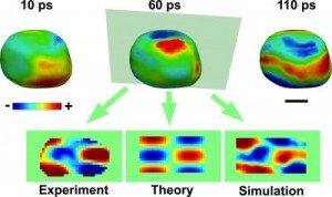
Caption: The acoustic phonons can be visualized on the surface as regions of contraction (blue) and expansion (red). Also shown are two-dimensional images comparing the experimental results with theory and molecular dynamics simulation. The scale bar is 100 nanometers. Credit: Jesse Clark/UCL

Caption: The acoustic phonons can be visualized on the surface as regions of contraction (blue) and expansion (red). Also shown are two-dimensional images comparing the experimental results with theory and molecular dynamics simulation. The scale bar is 100 nanometers. Credit: Jesse Clark/UCL

Here are more details from the news release,

Scientists found that the vibrations were unusual because they start off at exactly the same moment everywhere inside the crystal. It was previously expected that the effects of the excitation would travel across the gold nanocrystal at the speed of sound, but they were found to be much faster, i.e., supersonic.

The new images support theoretical models for light interaction with metals, where energy is first transferred to electrons, which are able to short-circuit the much slower motion of the atoms.

The team carried out the experiments at the SLAC National Accelerator Laboratory using a revolutionary X-ray laser called the “Linac Coherent Light Source”. The pulses of X-rays are extremely short (measured in femtoseconds, or quadrillionths of a second), meaning they are able to freeze all motion of the atoms in any sample, leaving only the electrons still moving.

However, the X-ray pulses are intense enough that the team was able to take single snapshots of the vibrations of the gold nanocrystals they were examining. The vibration was started with a short pulse of infrared light.

The real keeners can watch the movie if they click on the link to the May 23, 2013 news release on EurekAlert.

The team developing this movie was international in scope (from the news release),

The research team included contributors from UCL, University of Oxford, SLAC, Argonne National Laboratory [US] and LaTrobe University, Australia.

Shades of 1939! Advance in x-ray imaging of nanomaterials

The technique was first suggested in 1939 but wasn’t feasible until the advent of computers and their algorithms. Researchers at the University College of London have found a way to improve the quality of 3-D images of nanomaterials. From the Aug. 7, 2012 news release on EurekAlert,

A new advance in X-ray imaging has revealed the dramatic three-dimensional shape of gold nanocrystals, and is likely to shine a light on the structure of other nano-scale materials.

Described today in Nature Communications, the new technique improves the quality of nanomaterial images, made using X-ray diffraction, by accurately correcting distortions in the X-ray light.

Dr Jesse Clark, lead author of the study from the London Centre for Nanotechnology [at the University College of London] said: “With nanomaterials playing an increasingly important role in many applications, there is a real need to be able to obtain very high quality three dimensional images of these samples.

“Up until now we have been limited by the quality of our X-rays. Here we have demonstrated that with imperfect X-ray sources we can still obtain very high quality images of nanomaterials.”

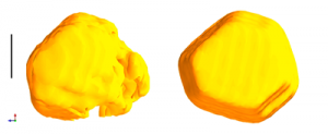
You can see the differences for yourself in this image provided by the researchers,

Figure: Shown on the left is the three dimensional image of a gold nanocrystal obtained previously while on the right is the image using the newly developed method. The features of the nanocrystal are vastly improved in the image on the left. The black scale bar is 100 nanometres (1 nanometre = 1 billionth of a meter). Downloaded from http://www.london-nano.com/research-and-facilities/highlight/advance-in-x-ray-imaging-shines-light-on-nanomaterials

The researchers have also provided two videos, the first features the current standard 3-D image of a gold nanocrystal and the second features the improved image,

Standard 3-D

Improved 3-D

The Aug. 7, 2012 news release originated from an article (Aug. 2012?) by Ian Robinson and Jesse Clark for the London Centre for Nanotechnology (part of the University College of London) giving context for the research and describing the technique (Note: I have removed a link),

Up until now, most nanomaterial imaging has been done using electron microscopy. X-ray imaging is an attractive alternative as X-rays penetrate further into the material than electrons and can be used in ambient or controlled environments.

However, making lenses that focus X-rays is very difficult. As an alternative, scientists use the indirect method of coherent diffraction imaging (CDI), where the diffraction pattern of the sample is measured (without lenses) and inverted to an image by computer.

Nobel Prize winner Lawrence Bragg suggested this method in 1939 but had no way to determine the missing phases of the diffraction, which are today provided by computer algorithms.

CDI can be performed very well at the latest synchrotron X-ray sources such as the UK’s Diamond Light Source which have much higher coherent flux than earlier machines.  CDI is gaining momentum in the study of nanomaterials, but, until now, has suffered from poor synchimage quality, with broken or non-uniform density.  This had been attributed to imperfect coherence of the X-ray light used.

The dramatic three-dimensional images of gold nanocrystals presented in this study demonstrate that this distortion can be corrected by appropriate modelling of the coherence function.

Professor Ian Robinson, London Centre for Nanotechnology and author of the paper said: “The corrected images are far more interpretable that ever obtained previously and will likely lead to new understanding of structure of nanoscale materials.”

The method should also work for free-electron-laser, electron- and atom-based diffractive imaging.

That mention of the UK’s Diamond Light Source reminded me of the Canadian Light Source located in Saskatoon, Saskatchewan. I imagine this work will open up some possibilities for the researchers there.

For those who would like to read more about the work, here’s a citation for the article,

High resolution three dimensional partially coherent diffraction imaging, Nature Communications.  J.N. Clark, X. Huang, R. Harder, & I.K. Robinson Nature Communications 3, Article number: 993 doi:10.1038/ncomms1994

This article is behind a paywall.