Tag Archives: Harvard John A. Paulson School of Engineering and Applied Sciences

Cyborg organoids?

Every time I think I’ve become inured to the idea of a fuzzy boundary between life and nonlife something new crosses my path such as integrating nanoelectronics with cells for cyborg organoids. An August 9, 2019 news item on ScienceDaily makes the announcement,

What happens in the early days of organ development? How do a small group of cells organize to become a heart, a brain, or a kidney? This critical period of development has long remained the black box of developmental biology, in part because no sensor was small or flexible enough to observe this process without damaging the cells.

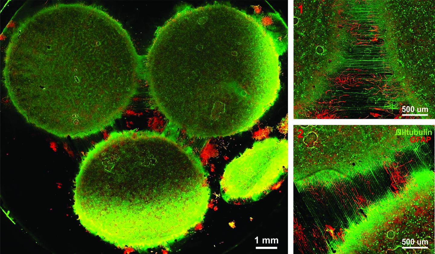
Now, researchers from the Harvard John A. Paulson School of Engineering and Applied Sciences (SEAS) have grown simplified organs known as organoids with fully integrated sensors. These so-called cyborg organoids offer a rare glimpse into the early stages of organ development.

An August 8, 2019 Harvard John A. Paulson School of Engineering and Applied Sciences news release (also on EurekAlert but published August 9, 2019) by Leah Burrows, which originated the news item, expands on the theme,

“I was so inspired by the natural organ development process in high school, in which 3D organs start from few cells in 2D structures. I think if we can develop nanoelectronics that are so flexible, stretchable, and soft that they can grow together with developing tissue through their natural development process, the embedded sensors can measure the entire activity of this developmental process,” said Jia Liu, Assistant Professor of Bioengineering at SEAS and senior author of the study. “The end result is a piece of tissue with a nanoscale device completely distributed and integrated across the entire three-dimensional volume of the tissue.”

This type of device emerges from the work that Liu began as a graduate student in the lab of Charles M. Lieber, the Joshua and Beth Friedman University Professor. In Lieber’s lab, Liu once developed flexible, mesh-like nanoelectronics that could be injected in specific regions of tissue.

Building on that design, Liu and his team increased the stretchability of the nanoelectronics by changing the shape of the mesh from straight lines to serpentine structures (similar structures are used in wearable electronics). Then, the team transferred the mesh nanoelectronics onto a 2D sheet of stem cells, where the cells covered and interwove with the nanoelectronics via cell-cell attraction forces. As the stem cells began to morph into a 3D structure, the nanoelectronics seamlessly reconfigured themselves along with the cells, resulting in fully-grown 3D organoids with embedded sensors.

The stem cells were then differentiated into cardiomyocytes — heart cells — and the researchers were able to monitor and record the electrophysiological activity for 90 days.

“This method allows us to continuously monitor the developmental process and understand how the dynamics of individual cells start to interact and synchronize during the entire developmental process,” said Liu. “It could be used to turn any organoid into cyborg organoids, including brain and pancreas organoids.”

In addition to helping answer fundamental questions about biology, cyborg organoids could be used to test and monitor patient-specific drug treatments and potentially used for transplantations.

Here’s a link to and a citation for the paper

Cyborg Organoids: Implantation of Nanoelectronics via Organogenesis for Tissue-Wide Electrophysiology by Qiang Li, Kewang Nan, Paul Le Floch, Zuwan Lin, Hao Sheng, Thomas S. Blum, Jia Liu. Nano Lett.20191985781-5789 DOI: https://doi.org/10.1021/acs.nanolett.9b02512 Publication Date:July 26, 2019 Copyright © 2019 American Chemical Society

This paper is behind a paywall.

What is a multiregional brain-on-a-chip?

In response to having created a multiregional brain-on-a-chip, there’s an explanation from the team at Harvard University (which answers my question) in a Jan. 13, 2017 Harvard John A. Paulson School of Engineering and Applied Sciences news release (also on EurekAlert) by Leah Burrows,

Harvard University researchers have developed a multiregional brain-on-a-chip that models the connectivity between three distinct regions of the brain. The in vitro model was used to extensively characterize the differences between neurons from different regions of the brain and to mimic the system’s connectivity.

“The brain is so much more than individual neurons,” said Ben Maoz, co-first author of the paper and postdoctoral fellow in the Disease Biophysics Group in the Harvard John A. Paulson School of Engineering and Applied Sciences (SEAS). “It’s about the different types of cells and the connectivity between different regions of the brain. When modeling the brain, you need to be able to recapitulate that connectivity because there are many different diseases that attack those connections.”

“Roughly twenty-six percent of the US healthcare budget is spent on neurological and psychiatric disorders,” said Kit Parker, the Tarr Family Professor of Bioengineering and Applied Physics Building at SEAS and Core Faculty Member of the Wyss Institute for Biologically Inspired Engineering at Harvard University. “Tools to support the development of therapeutics to alleviate the suffering of these patients is not only the human thing to do, it is the best means of reducing this cost.”

Researchers from the Disease Biophysics Group at SEAS and the Wyss Institute modeled three regions of the brain most affected by schizophrenia — the amygdala, hippocampus and prefrontal cortex.

They began by characterizing the cell composition, protein expression, metabolism, and electrical activity of neurons from each region in vitro.

“It’s no surprise that neurons in distinct regions of the brain are different but it is surprising just how different they are,” said Stephanie Dauth, co-first author of the paper and former postdoctoral fellow in the Disease Biophysics Group. “We found that the cell-type ratio, the metabolism, the protein expression and the electrical activity all differ between regions in vitro. This shows that it does make a difference which brain region’s neurons you’re working with.”

Next, the team looked at how these neurons change when they’re communicating with one another. To do that, they cultured cells from each region independently and then let the cells establish connections via guided pathways embedded in the chip.

The researchers then measured cell composition and electrical activity again and found that the cells dramatically changed when they were in contact with neurons from different regions.

“When the cells are communicating with other regions, the cellular composition of the culture changes, the electrophysiology changes, all these inherent properties of the neurons change,” said Maoz. “This shows how important it is to implement different brain regions into in vitro models, especially when studying how neurological diseases impact connected regions of the brain.”

To demonstrate the chip’s efficacy in modeling disease, the team doped different regions of the brain with the drug Phencyclidine hydrochloride — commonly known as PCP — which simulates schizophrenia. The brain-on-a-chip allowed the researchers for the first time to look at both the drug’s impact on the individual regions as well as its downstream effect on the interconnected regions in vitro.

The brain-on-a-chip could be useful for studying any number of neurological and psychiatric diseases, including drug addiction, post traumatic stress disorder, and traumatic brain injury.

“To date, the Connectome project has not recognized all of the networks in the brain,” said Parker. “In our studies, we are showing that the extracellular matrix network is an important part of distinguishing different brain regions and that, subsequently, physiological and pathophysiological processes in these brain regions are unique. This advance will not only enable the development of therapeutics, but fundamental insights as to how we think, feel, and survive.”

Here’s an image from the researchers,

Caption: Image of the in vitro model showing three distinct regions of the brain connected by axons. Credit: Disease Biophysics Group/Harvard University

Here’s a link to and a citation for the paper,

Neurons derived from different brain regions are inherently different in vitro: A novel multiregional brain-on-a-chip by Stephanie Dauth, Ben M Maoz, Sean P Sheehy, Matthew A Hemphill, Tara Murty, Mary Kate Macedonia, Angie M Greer, Bogdan Budnik, Kevin Kit Parker. Journal of Neurophysiology Published 28 December 2016 Vol. no. [?] , DOI: 10.1152/jn.00575.2016

This paper is behind a paywall and they haven’t included the vol. no. in the citation I’ve found.

Printing in midair

Dexter Johnson’s May 16, 2016 posting on his Nanoclast blog (on the IEEE [Institute of Electrical and Electronics Engineers] website) was my first introduction to something wonder-inducing (Note: Links have been removed),

While the growth of 3-D printing has led us to believe we can produce just about any structure with it, the truth is that it still falls somewhat short.

Researchers at Harvard University are looking to realize a more complete range of capabilities for 3-D printing in fabricating both planar and freestanding 3-D structures and do it relatively quickly and on low-cost plastic substrates.

In research published in the journal Proceedings of the National Academy of Sciences (PNAS),  the researchers extruded a silver-nanoparticle ink and annealed it with a laser so quickly that the system let them easily “write” free-standing 3-D structures.

While this may sound humdrum, what really takes one’s breath away with this technique is that it can create 3-D structures seemingly suspended in air without any signs of support as though they were drawn there with a pen.

Laser-assisted direct ink writing allowed this delicate 3D butterfly to be printed without any auxiliary support structure (Image courtesy of the Lewis Lab/Harvard University)

Laser-assisted direct ink writing allowed this delicate 3D butterfly to be printed without any auxiliary support structure (Image courtesy of the Lewis Lab/Harvard University)

A May 16, 2016 Harvard University press release (also on EurekAlert) provides more detail about the work,

“Flat” and “rigid” are terms typically used to describe electronic devices. But the increasing demand for flexible, wearable electronics, sensors, antennas and biomedical devices has led a team at Harvard’s John A. Paulson School of Engineering and Applied Sciences (SEAS) and Wyss Institute for Biologically Inspired Engineering to innovate an eye-popping new way of printing complex metallic architectures – as though they are seemingly suspended in midair.

“I am truly excited by this latest advance from our lab, which allows one to 3D print and anneal flexible metal electrodes and complex architectures ‘on-the-fly,’ ” said Lewis [Jennifer Lewis, the Hansjörg Wyss Professor of Biologically Inspired Engineering at SEAS and Wyss Core Faculty member].

Lewis’ team used an ink composed of silver nanoparticles, sending it through a printing nozzle and then annealing it using a precisely programmed laser that applies just the right amount of energy to drive the ink’s solidification. The printing nozzle moves along x, y, and z axes and is combined with a rotary print stage to enable freeform curvature. In this way, tiny hemispherical shapes, spiral motifs, even a butterfly made of silver wires less than the width of a hair can be printed in free space within seconds. The printed wires exhibit excellent electrical conductivity, almost matching that of bulk silver.

When compared to conventional 3D printing techniques used to fabricate conductive metallic features, laser-assisted direct ink writing is not only superior in its ability to produce curvilinear, complex wire patterns in one step, but also in the sense that localized laser heating enables electrically conductive silver wires to be printed directly on low-cost plastic substrates.

According to the study’s first author, Wyss Institute Postdoctoral Fellow Mark Skylar-Scott, Ph.D., the most challenging aspect of honing the technique was optimizing the nozzle-to-laser separation distance.

“If the laser gets too close to the nozzle during printing, heat is conducted upstream which clogs the nozzle with solidified ink,” said Skylar-Scott. “To address this, we devised a heat transfer model to account for temperature distribution along a given silver wire pattern, allowing us to modulate the printing speed and distance between the nozzle and laser to elegantly control the laser annealing process ‘on the fly.’ ”

The result is that the method can produce not only sweeping curves and spirals but also sharp angular turns and directional changes written into thin air with silver inks, opening up near limitless new potential applications in electronic and biomedical devices that rely on customized metallic architectures.

Seeing is believing, eh?

Here’s a link to and a citation for the paper,

Laser-assisted direct ink writing of planar and 3D metal architectures by Mark A. Skylar-Scott, Suman Gunasekaran, and Jennifer A. Lewis. PNAS [Proceedings of the National Academy of Sciences] 2016 doi: 10.1073/pnas.1525131113

I believe this paper is open access.

A question: I wonder what conditions are necessary before you can 3D print something in midair? Much as I’m dying to try this at home, I’m pretty that’s not possible.

Tune your windows for privacy

Caption: With an applied voltage, the nanowires on either side of the glass become attracted to each other and move toward each other, squeezing and deforming the soft elastomer. Because the nanowires are scattered unevenly across the surface, the elastomer deforms unevenly. That uneven roughness causes light to scatter, turning the glass opaque. Credit: David Clarke/Harvard SEAS [School of Engineering and Applied Sciences]

Right now, this is my favourite science illustration. A March 14, 2016 news item on Nanowerk announces Harvard’s new technology that can turn a clear window into an opaque one at the touch of a switch,

Say goodbye to blinds.

Researchers at the Harvard John A. Paulson School of Engineering and Applied Sciences have developed a technique that can quickly change the opacity of a window, turning it cloudy, clear or somewhere in between with the flick of a switch.

Tunable windows aren’t new but most previous technologies have relied on electrochemical reactions achieved through expensive manufacturing. This technology, developed by David Clarke, the Extended Tarr Family Professor of Materials, and postdoctoral fellow Samuel Shian, uses geometry [to] adjust the transparency of a window.

A March 14, 2016 Harvard University news release (also on EurekAlert) by Leah Burrows, which originated the news item, describes the technology in more detail,

The tunable window is comprised of a sheet of glass or plastic, sandwiched between transparent, soft elastomers sprayed with a coating of silver nanowires, too small to scatter light on their own.

But apply an electric voltage and things change quickly.

With an applied voltage, the nanowires on either side of the glass are energized to move toward each other, squeezing and deforming the soft elastomer. Because the nanowires are distributed unevenly across the surface, the elastomer deforms unevenly. The resulting uneven roughness causes light to scatter, turning the glass opaque.

The change happens in less than a second.

It’s like a frozen pond, said Shian.

“If the frozen pond is smooth, you can see through the ice. But if the ice is heavily scratched, you can’t see through,” said Shian.

Clarke and Shian found that the roughness of the elastomer surface depended on the voltage, so if you wanted a window that is only light clouded, you would apply less voltage than if you wanted a totally opaque window.

“Because this is a physical phenomenon rather than based on a chemical reaction, it is a simpler and potentially cheaper way to achieve commercial tunable windows,” said Clarke.

Current chemical-based controllable windows use vacuum deposition to coat the glass, a process that deposits layers of a material molecule by molecule. It’s expensive and painstaking. In Clarke and Shian’s method, the nanowire layer can be sprayed or peeled onto the elastomer, making the technology scalable for larger architectural projects.

Next the team is working on incorporating thinner elastomers, which would require lower voltages, more suited for standard electronical supplies.

Here’s a link to and a citation for the paper,

Electrically tunable window device by Samuel Shian and David R. Clarke. Optics Letters Vol. 41, Issue 6, pp. 1289-1292 (2016) •doi: 10.1364/OL.41.001289

This is an open access paper.