Tag Archives: IEEE

Drive to operationalize transistors that outperform silicon gets a boost

Dexter Johnson has written a Jan. 19, 2017 posting on his Nanoclast blog (on the IEEE [Institute of Electrical and Electronics Engineers]) about work which could lead to supplanting silicon-based transistors with carbon nanotube-based transistors in the future (Note: Links have been removed),

The end appears nigh for scaling down silicon-based complimentary metal-oxide semiconductor (CMOS) transistors, with some experts seeing the cutoff date as early as 2020.

While carbon nanotubes (CNTs) have long been among the nanomaterials investigated to serve as replacement for silicon in CMOS field-effect transistors (FETs) in a post-silicon future, they have always been bogged down by some frustrating technical problems. But, with some of the main technical showstoppers having been largely addressed—like sorting between metallic and semiconducting carbon nanotubes—the stage has been set for CNTs to start making their presence felt a bit more urgently in the chip industry.

Peking University scientists in China have now developed carbon nanotube field-effect transistors (CNT FETs) having a critical dimension—the gate length—of just five nanometers that would outperform silicon-based CMOS FETs at the same scale. The researchers claim in the journal Science that this marks the first time that sub-10 nanometer CNT CMOS FETs have been reported.

More importantly than just being the first, the Peking group showed that their CNT-based FETs can operate faster and at a lower supply voltage than their silicon-based counterparts.

A Jan. 20, 2017 article by Bob Yirka for phys.org provides more insight into the work at Peking University,

One of the most promising candidates is carbon nanotubes—due to their unique properties, transistors based on them could be smaller, faster and more efficient. Unfortunately, the difficulty in growing carbon nanotubes and their sometimes persnickety nature means that a way to make them and mass produce them has not been found. In this new effort, the researchers report on a method of creating carbon nanotube transistors that are suitable for testing, but not mass production.

To create the transistors, the researchers took a novel approach—instead of growing carbon nanotubes that had certain desired properties, they grew some and put them randomly on a silicon surface and then added electronics that would work with the properties they had—clearly not a strategy that would work for mass production, but one that allowed for building a carbon nanotube transistor that could be tested to see if it would verify theories about its performance. Realizing there would still be scaling problems using traditional electrodes, the researchers built a new kind by etching very tiny sheets of graphene. The result was a very tiny transistor, the team reports, capable of moving more current than a standard CMOS transistor using just half of the normal amount of voltage. It was also faster due to a much shorter switch delay, courtesy of a gate capacitance of just 70 femtoseconds.

Peking University has published an edited and more comprehensive version of the phys.org article first reported by Lisa Zyga and edited by Arthars,

Now in a new paper published in Nano Letters, researchers Tian Pei, et al., at Peking University in Beijing, China, have developed a modular method for constructing complicated integrated circuits (ICs) made from many FETs on individual CNTs. To demonstrate, they constructed an 8-bits BUS system–a circuit that is widely used for transferring data in computers–that contains 46 FETs on six CNTs. This is the most complicated CNT IC fabricated to date, and the fabrication process is expected to lead to even more complex circuits.

SEM image of an eight-transistor (8-T) unit that was fabricated on two CNTs (marked with two white dotted lines). The scale bar is 100 μm. (Copyright: 2014 American Chemical Society)

Ever since the first CNT FET was fabricated in 1998, researchers have been working to improve CNT-based electronics. As the scientists explain in their paper, semiconducting CNTs are promising candidates for replacing silicon wires because they are thinner, which offers better scaling-down potential, and also because they have a higher carrier mobility, resulting in higher operating speeds.

Yet CNT-based electronics still face challenges. One of the most significant challenges is obtaining arrays of semiconducting CNTs while removing the less-suitable metallic CNTs. Although scientists have devised a variety of ways to separate semiconducting and metallic CNTs, these methods almost always result in damaged semiconducting CNTs with degraded performance.

To get around this problem, researchers usually build ICs on single CNTs, which can be individually selected based on their condition. It’s difficult to use more than one CNT because no two are alike: they each have slightly different diameters and properties that affect performance. However, using just one CNT limits the complexity of these devices to simple logic and arithmetical gates.

The 8-T unit can be used as the basic building block of a variety of ICs other than BUS systems, making this modular method a universal and efficient way to construct large-scale CNT ICs. Building on their previous research, the scientists hope to explore these possibilities in the future.

“In our earlier work, we showed that a carbon nanotube based field-effect transistor is about five (n-type FET) to ten (p-type FET) times faster than its silicon counterparts, but uses much less energy, about a few percent of that of similar sized silicon transistors,” Peng said.

“In the future, we plan to construct large-scale integrated circuits that outperform silicon-based systems. These circuits are faster, smaller, and consume much less power. They can also work at extremely low temperatures (e.g., in space) and moderately high temperatures (potentially no cooling system required), on flexible and transparent substrates, and potentially be bio-compatible.”

Here’s a link to and a citation for the paper,

Scaling carbon nanotube complementary transistors to 5-nm gate lengths by Chenguang Qiu, Zhiyong Zhang, Mengmeng Xiao, Yingjun Yang, Donglai Zhong, Lian-Mao Peng. Science  20 Jan 2017: Vol. 355, Issue 6322, pp. 271-276 DOI: 10.1126/science.aaj1628

This paper is behind a paywall.

Nanotechnology cracks Wall Street (Daily)

David Dittman’s Jan. 11, 2017 article for wallstreetdaily.com portrays a great deal of excitement about nanotechnology and the possibilities (I’m highlighting the article because it showcases Dexter Johnson’s Nanoclast blog),

When we talk about next-generation aircraft, next-generation wearable biomedical devices, and next-generation fiber-optic communication, the consistent theme is nano: nanotechnology, nanomaterials, nanophotonics.

For decades, manufacturers have used carbon fiber to make lighter sports equipment, stronger aircraft, and better textiles.

Now, as Dexter Johnson of IEEE [Institute of Electrical and Electronics Engineers] Spectrum reports [on his Nanoclast blog], carbon nanotubes will help make aerospace composites more efficient:

Now researchers at the University of Surrey’s Advanced Technology Institute (ATI), the University of Bristol’s Advanced Composite Centre for Innovation and Science (ACCIS), and aerospace company Bombardier [headquartered in Montréal, Canada] have collaborated on the development of a carbon nanotube-enabled material set to replace the polymer sizing. The reinforced polymers produced with this new material have enhanced electrical and thermal conductivity, opening up new functional possibilities. It will be possible, say the British researchers, to embed gadgets such as sensors and energy harvesters directly into the material.

When it comes to flight, lighter is better, so building sensors and energy harvesters into the body of aircraft marks a significant leap forward.

Johnson also reports for IEEE Spectrum on a “novel hybrid nanomaterial” based on oscillations of electrons — a major advance in nanophotonics:

Researchers at the University of Texas at Austin have developed a hybrid nanomaterial that enables the writing, erasing and rewriting of optical components. The researchers believe that this nanomaterial and the techniques used in exploiting it could create a new generation of optical chips and circuits.

Of course, the concept of rewritable optics is not altogether new; it forms the basis of optical storage mediums like CDs and DVDs. However, CDs and DVDs require bulky light sources, optical media and light detectors. The advantage of the rewritable integrated photonic circuits developed here is that it all happens on a 2-D material.

“To develop rewritable integrated nanophotonic circuits, one has to be able to confine light within a 2-D plane, where the light can travel in the plane over a long distance and be arbitrarily controlled in terms of its propagation direction, amplitude, frequency and phase,” explained Yuebing Zheng, a professor at the University of Texas who led the research… “Our material, which is a hybrid, makes it possible to develop rewritable integrated nanophotonic circuits.”

Who knew that mixing graphene with homemade Silly Putty would create a potentially groundbreaking new material that could make “wearables” actually useful?

Next-generation biomedical devices will undoubtedly include some of this stuff:

A dash of graphene can transform the stretchy goo known as Silly Putty into a pressure sensor able to monitor a human pulse or even track the dainty steps of a small spider.

The material, dubbed G-putty, could be developed into a device that continuously monitors blood pressure, its inventors hope.

The guys who made G-putty often rely on “household stuff” in their research.

It’s nice to see a blogger’s work be highlighted. Congratulations Dexter.

G-putty was mentioned here in a Dec. 30, 2016 posting which also includes a link to Dexter’s piece on the topic.

Keeping up with science is impossible: ruminations on a nanotechnology talk

I think it’s time to give this suggestion again. Always hold a little doubt about the science information you read and hear. Everybody makes mistakes.

Here’s an example of what can happen. George Tulevski who gave a talk about nanotechnology in Nov. 2016 for TED@IBM is an accomplished scientist who appears to have made an error during his TED talk. From Tulevski’s The Next Step in Nanotechnology talk transcript page,

When I was a graduate student, it was one of the most exciting times to be working in nanotechnology. There were scientific breakthroughs happening all the time. The conferences were buzzing, there was tons of money pouring in from funding agencies. And the reason is when objects get really small, they’re governed by a different set of physics that govern ordinary objects, like the ones we interact with. We call this physics quantum mechanics. [emphases mine] And what it tells you is that you can precisely tune their behavior just by making seemingly small changes to them, like adding or removing a handful of atoms, or twisting the material. It’s like this ultimate toolkit. You really felt empowered; you felt like you could make anything.

In September 2016, scientists at Cambridge University (UK) announced they had concrete proof that the physics governing materials at the nanoscale is unique, i.e., it does not follow the rules of either classical or quantum physics. From my Oct. 27, 2016 posting,

A Sept. 29, 2016 University of Cambridge press release, which originated the news item, hones in on the peculiarities of the nanoscale,

In the middle, on the order of around 10–100,000 molecules, something different is going on. Because it’s such a tiny scale, the particles have a really big surface-area-to-volume ratio. This means the energetics of what goes on at the surface become very important, much as they do on the atomic scale, where quantum mechanics is often applied.

Classical thermodynamics breaks down. But because there are so many particles, and there are many interactions between them, the quantum model doesn’t quite work either.

It is very, very easy to miss new developments no matter how tirelessly you scan for information.

Tulevski is a good, interesting, and informed speaker but I do have one other hesitation regarding his talk. He seems to think that over the last 15 years there should have been more practical applications arising from the field of nanotechnology. There are two aspects here. First, he seems to be dating the ‘nanotechnology’ effort from the beginning of the US National Nanotechnology Initiative and there are many scientists who would object to that as the starting point. Second, 15 or even 30 or more years is a brief period of time especially when you are investigating that which hasn’t been investigated before. For example, you might want to check out the book, “Leviathan and the Air-Pump: Hobbes, Boyle, and the Experimental Life” (published 1985) is a book by Steven Shapin and Simon Schaffer (Wikipedia entry for the book). The amount of time (years) spent on how to make just the glue which held the various experimental apparatuses together was a revelation to me. Of  course, it makes perfect sense that if you’re trying something new, you’re going to have figure out everything.

By the way, I include my blog as one of the sources of information that can be faulty despite efforts to make corrections and to keep up with the latest. Even the scientists at Cambridge University can run into some problems as I noted in my Jan. 28, 2016 posting.

Getting back to Tulevsk, herei’s a link to his lively, informative talk :
https://www.ted.com/talks/george_tulevski_the_next_step_in_nanotechnology#t-562570

ETA Jan. 24, 2017: For some insight into how uncertain, tortuous, and expensive commercializing technology can be read Dexter Johnson’s Jan. 23, 2017 posting on his Nanoclast blog (on the IEEE [Institute of Electrical and Electronics Engineers] website). Here’s an excerpt (Note: Links have been removed),

The brief description of this odyssey includes US $78 million in financing over 15 years and $50 million in revenues over that period through licensing of its technology and patents. That revenue includes a back-against-the-wall sell-off of a key business unit to Lockheed Martin in 2008.  Another key moment occured back in 2012 when Belgian-based nanoelectronics powerhouse Imec took on the job of further developing Nantero’s carbon-nanotube-based memory back in 2012. Despite the money and support from major electronics players, the big commercial breakout of their NRAM technology seemed ever less likely to happen with the passage of time.

Colours in bendable electronic paper

Scientists at Chalmers University of Technology (Sweden) are able to produce a rainbow of colours in a new electronic paper according to an Oct. 14, 2016 news item on Nanowerk,

Less than a micrometre thin, bendable and giving all the colours that a regular LED display does, it still needs ten times less energy than a Kindle tablet. Researchers at Chalmers University of Technology have developed the basis for a new electronic “paper.”

When Chalmers researcher Andreas Dahlin and his PhD student Kunli Xiong were working on placing conductive polymers on nanostructures, they discovered that the combination would be perfectly suited to creating electronic displays as thin as paper. A year later the results were ready for publication. A material that is less than a micrometre thin, flexible and giving all the colours that a standard LED display does.

An Oct. 14, 2016 Chalmers University of Technology press release (also on EurekAlert) by Mats Tiborn, which originated the news item, expands on the theme,

“The ’paper’ is similar to the Kindle tablet. It isn’t lit up like a standard display, but rather reflects the external light which illuminates it. Therefore it works very well where there is bright light, such as out in the sun, in contrast to standard LED displays that work best in darkness. At the same time it needs only a tenth of the energy that a Kindle tablet uses, which itself uses much less energy than a tablet LED display”, says Andreas Dahlin.

It all depends on the polymers’ ability to control how light is absorbed and reflected. The polymers that cover the whole surface lead the electric signals throughout the full display and create images in high resolution. The material is not yet ready for application, but the basis is there. The team has tested and built a few pixels. These use the same red, green and blue (RGB) colours that together can create all the colours in standard LED displays. The results so far have been positive, what remains now is to build pixels that cover an area as large as a display.

“We are working at a fundamental level but even so, the step to manufacturing a product out of it shouldn’t be too far away. What we need now are engineers”, says Andreas Dahlin.

One obstacle today is that there is gold and silver in the display.

“The gold surface is 20 nanometres thick so there is not that much gold in it. But at present there is a lot of gold wasted in manufacturing it. Either we reduce the waste or we find another way to reduce the production cost”, says Andreas Dahlin.

Caption: Chalmers' e-paper contains gold, silver and PET plastic. The layer that produces the colours is less than a micrometre thin. Credit: Mats Tiborn

Caption: Chalmers’ e-paper contains gold, silver and PET plastic. The layer that produces the colours is less than a micrometre thin. Credit: Mats Tiborn

Here’s a link to and a citation for the paper,

Plasmonic Metasurfaces with Conjugated Polymers for Flexible Electronic Paper in Color by Kunli Xiong, Gustav Emilsson, Ali Maziz, Xinxin Yang, Lei Shao, Edwin W. H. Jager, and Andreas B. Dahlin. Advanced Materials DOI: 10.1002/adma.201603358 Version of Record online: 27 SEP 2016

© 2016 WILEY-VCH Verlag GmbH & Co. KGaA, Weinheim

This paper is behind a paywall.

Finally, Dexter Johnson in an Oct. 18, 2016 posting on his Nanoclast blog (on the IEEE [Institute of Electrical and Electronics Engineers] website) offers some broader insight into this development (Note: Links have been removed),

Plasmonic nanostructures leverage the oscillations in the density of electrons that are generated when photons hit a metal surface. Researchers have used these structures for applications including increasing the light absorption of solar cells and creating colors without the need for dyes. As a demonstration of how effective these nanostructures are as a replacement for color dyes, a the technology has been used to produce a miniature copy of the Mona Lisa in a space smaller than the footprint taken up by a single pixel on an iPhone Retina display.

Cooling the skin with plastic clothing

Rather that cooling or heating an entire room, why not cool or heat the person? Engineers at Stanford University (California, US) have developed a material that helps with half of that premise: cooling. From a Sept. 1, 2016 news item on ScienceDaily,

Stanford engineers have developed a low-cost, plastic-based textile that, if woven into clothing, could cool your body far more efficiently than is possible with the natural or synthetic fabrics in clothes we wear today.

Describing their work in Science, the researchers suggest that this new family of fabrics could become the basis for garments that keep people cool in hot climates without air conditioning.

“If you can cool the person rather than the building where they work or live, that will save energy,” said Yi Cui, an associate professor of materials science and engineering and of photon science at Stanford.

A Sept. 1, 2016 Stanford University news release (also on EurekAlert) by Tom Abate, which originated the news item, further explains the information in the video,

This new material works by allowing the body to discharge heat in two ways that would make the wearer feel nearly 4 degrees Fahrenheit cooler than if they wore cotton clothing.

The material cools by letting perspiration evaporate through the material, something ordinary fabrics already do. But the Stanford material provides a second, revolutionary cooling mechanism: allowing heat that the body emits as infrared radiation to pass through the plastic textile.

All objects, including our bodies, throw off heat in the form of infrared radiation, an invisible and benign wavelength of light. Blankets warm us by trapping infrared heat emissions close to the body. This thermal radiation escaping from our bodies is what makes us visible in the dark through night-vision goggles.

“Forty to 60 percent of our body heat is dissipated as infrared radiation when we are sitting in an office,” said Shanhui Fan, a professor of electrical engineering who specializes in photonics, which is the study of visible and invisible light. “But until now there has been little or no research on designing the thermal radiation characteristics of textiles.”

Super-powered kitchen wrap

To develop their cooling textile, the Stanford researchers blended nanotechnology, photonics and chemistry to give polyethylene – the clear, clingy plastic we use as kitchen wrap – a number of characteristics desirable in clothing material: It allows thermal radiation, air and water vapor to pass right through, and it is opaque to visible light.

The easiest attribute was allowing infrared radiation to pass through the material, because this is a characteristic of ordinary polyethylene food wrap. Of course, kitchen plastic is impervious to water and is see-through as well, rendering it useless as clothing.

The Stanford researchers tackled these deficiencies one at a time.

First, they found a variant of polyethylene commonly used in battery making that has a specific nanostructure that is opaque to visible light yet is transparent to infrared radiation, which could let body heat escape. This provided a base material that was opaque to visible light for the sake of modesty but thermally transparent for purposes of energy efficiency.

They then modified the industrial polyethylene by treating it with benign chemicals to enable water vapor molecules to evaporate through nanopores in the plastic, said postdoctoral scholar and team member Po-Chun Hsu, allowing the plastic to breathe like a natural fiber.

Making clothes

That success gave the researchers a single-sheet material that met their three basic criteria for a cooling fabric. To make this thin material more fabric-like, they created a three-ply version: two sheets of treated polyethylene separated by a cotton mesh for strength and thickness.

To test the cooling potential of their three-ply construct versus a cotton fabric of comparable thickness, they placed a small swatch of each material on a surface that was as warm as bare skin and measured how much heat each material trapped.

“Wearing anything traps some heat and makes the skin warmer,” Fan said. “If dissipating thermal radiation were our only concern, then it would be best to wear nothing.”

The comparison showed that the cotton fabric made the skin surface 3.6 F warmer than their cooling textile. The researchers said this difference means that a person dressed in their new material might feel less inclined to turn on a fan or air conditioner.

The researchers are continuing their work on several fronts, including adding more colors, textures and cloth-like characteristics to their material. Adapting a material already mass produced for the battery industry could make it easier to create products.

“If you want to make a textile, you have to be able to make huge volumes inexpensively,” Cui said.

Fan believes that this research opens up new avenues of inquiry to cool or heat things, passively, without the use of outside energy, by tuning materials to dissipate or trap infrared radiation.

“In hindsight, some of what we’ve done looks very simple, but it’s because few have really been looking at engineering the radiation characteristics of textiles,” he said.

Dexter Johnson (Nanoclast blog on the IEEE [Institute of Electrical and Electronics Engineers] website) has written a Sept. 2, 2016 posting where he provides more technical detail about this work,

The nanoPE [nanoporous polyethylene] material is able to achieve this release of the IR heat because of the size of the interconnected pores. The pores can range in size from 50 to 1000 nanometers. They’re therefore comparable in size to wavelengths of visible light, which allows the material to scatter that light. However, because the pores are much smaller than the wavelength of infrared light, the nanoPE is transparent to the IR.

It is this combination of blocking visible light and allowing IR to pass through that distinguishes the nanoPE material from regular polyethylene, which allows similar amounts of IR to pass through, but can only block 20 percent of the visible light compared to nanoPE’s 99 percent opacity.

The Stanford researchers were also able to improve on the water wicking capability of the nanoPE material by using a microneedle punching technique and coating the material with a water-repelling agent. The result is that perspiration can evaporate through the material unlike with regular polyethylene.

For those who wish to further pursue their interest, Dexter has a lively writing style and he provides more detail and insight in his posting.

Here’s a link to and a citation for the paper,

Radiative human body cooling by nanoporous polyethylene textile by Po-Chun Hsu, Alex Y. Song, Peter B. Catrysse, Chong Liu, Yucan Peng, Jin Xie, Shanhui Fan, Yi Cui. Science  02 Sep 2016: Vol. 353, Issue 6303, pp. 1019-1023 DOI: 10.1126/science.aaf5471

This paper is open access.

First carbon nanotube mirrors for Cubesat telescope

A July 12, 2016 news item on phys.org describes a project that could lead to the first carbon nanotube mirrors to be used in a Cubesat telescope in space,

A lightweight telescope that a team of NASA scientists and engineers is developing specifically for CubeSat scientific investigations could become the first to carry a mirror made of carbon nanotubes in an epoxy resin.

Led by Theodor Kostiuk, a scientist at NASA’s [US National Aeronautics and Space Administration] Goddard Space Flight Center in Greenbelt, Maryland, the technology-development effort is aimed at giving the scientific community a compact, reproducible, and relatively inexpensive telescope that would fit easily inside a CubeSat. Individual CubeSats measure four inches on a side.

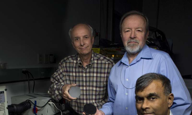
John Kolasinski (left), Ted Kostiuk (center), and Tilak Hewagama (right) hold mirrors made of carbon nanotubes in an epoxy resin. The mirror is being tested for potential use in a lightweight telescope specifically for CubeSat scientific investigations. Credit: NASA/W. Hrybyk

John Kolasinski (left), Ted Kostiuk (center), and Tilak Hewagama (right) hold mirrors made of carbon nanotubes in an epoxy resin. The mirror is being tested for potential use in a lightweight telescope specifically for CubeSat scientific investigations. Credit: NASA/W. Hrybyk

A July 12, 2016 US National Aeronautics and Space Administration (NASA) news release, which originated the news item, provides more information about Cubesats,

Small satellites, including CubeSats, are playing an increasingly larger role in exploration, technology demonstration, scientific research and educational investigations at NASA. These miniature satellites provide a low-cost platform for NASA missions, including planetary space exploration; Earth observations; fundamental Earth and space science; and developing precursor science instruments like cutting-edge laser communications, satellite-to-satellite communications and autonomous movement capabilities. They also allow an inexpensive means to engage students in all phases of satellite development, operation and exploitation through real-world, hands-on research and development experience on NASA-funded rideshare launch opportunities.

Under this particular R&D effort, Kostiuk’s team seeks to develop a CubeSat telescope that would be sensitive to the ultraviolet, visible, and infrared wavelength bands. It would be equipped with commercial-off-the-shelf spectrometers and imagers and would be ideal as an “exploratory tool for quick looks that could lead to larger missions,” Kostiuk explained. “We’re trying to exploit commercially available components.”

While the concept won’t get the same scientific return as say a flagship-style mission or a large, ground-based telescope, it could enable first order of scientific investigations or be flown as a constellation of similarly equipped CubeSats, added Kostiuk.

With funding from Goddard’s Internal Research and Development program, the team has created a laboratory optical bench made up of three commercially available, miniaturized spectrometers optimized for the ultraviolet, visible, and near-infrared wavelength bands. The spectrometers are connected via fiber optic cables to the focused beam of a three-inch diameter carbon-nanotube mirror. The team is using the optical bench to test the telescope’s overall design.

The news release then describes the carbon nanotube mirrors,

By all accounts, the new-fangled mirror could prove central to creating a low-cost space telescope for a range of CubeSat scientific investigations.

Unlike most telescope mirrors made of glass or aluminum, this particular optic is made of carbon nanotubes embedded in an epoxy resin. Sub-micron-size, cylindrically shaped, carbon nanotubes exhibit extraordinary strength and unique electrical properties, and are efficient conductors of heat. Owing to these unusual properties, the material is valuable to nanotechnology, electronics, optics, and other fields of materials science, and, as a consequence, are being used as additives in various structural materials.

“No one has been able to make a mirror using a carbon-nanotube resin,” said Peter Chen, a Goddard contractor and president of Lightweight Telescopes, Inc., a Columbia, Maryland-based company working with the team to create the CubeSat-compatible telescope.

“This is a unique technology currently available only at Goddard,” he continued. “The technology is too new to fly in space, and first must go through the various levels of technological advancement. But this is what my Goddard colleagues (Kostiuk, Tilak Hewagama, and John Kolasinski) are trying to accomplish through the CubeSat program.”

The use of a carbon-nanotube optic in a CubeSat telescope offers a number of advantages, said Hewagama, who contacted Chen upon learning of a NASA Small Business Innovative Research program awarded to Chen’s company to further advance the mirror technology. In addition to being lightweight, highly stable, and easily reproducible, carbon-nanotube mirrors do not require polishing — a time-consuming and often times expensive process typically required to assure a smooth, perfectly shaped mirror, said Kolasinski, an engineer and science collaborator on the project.

To make a mirror, technicians simply pour the mixture of epoxy and carbon nanotubes into a mandrel or mold fashioned to meet a particular optical prescription. They then heat the mold to to cure and harden the epoxy. Once set, the mirror then is coated with a reflective material of aluminum and silicon dioxide.

“After making a specific mandrel or mold, many tens of identical low-mass, highly uniform replicas can be produced at low cost,” Chen said. “Complete telescope assemblies can be made this way, which is the team’s main interest. For the CubeSat program, this capability will enable many spacecraft to be equipped with identical optics and different detectors for a variety of experiments. They also can be flown in swarms and constellations.”

There could be other applications for these carbon nanotube mirrors according to the news release,

A CubeSat telescope is one possible application for the optics technology, Chen added.

He believes it also would work for larger telescopes, particularly those comprised of multiple mirror segments. Eighteen hexagonal-shape mirrors, for example, form the James Webb Space Telescope’s 21-foot primary mirror and each of the twin telescopes at the Keck Observatory in Mauna Kea, Hawaii, contain 36 segments to form a 32-foot mirror.

Many of the mirror segments in these telescopes are identical and can therefore be produced using a single mandrel. This approach avoids the need to grind and polish many individual segments to the same shape and focal length, thus potentially leading to significant savings in schedule and cost.

Moreover, carbon-nanotube mirrors can be made into ‘smart optics’. To maintain a single perfect focus in the Keck telescopes, for example, each mirror segment has several externally mounted actuators that deform the mirrors into the specific shapes required at different telescope orientations.

In the case of carbon-nanotube mirrors, the actuators can be formed into the optics at the time of fabrication. This is accomplished by applying electric fields to the resin mixture before cure, which leads to the formation of carbon-nanotube chains and networks. After curing, technicians then apply power to the mirror, thereby changing the shape of the optical surface. This concept has already been proven in the laboratory.

“This technology can potentially enable very large-area technically active optics in space,” Chen said. “Applications address everything from astronomy and Earth observing to deep-space communications.”

Dexter Johnson provides some additional tidbits in his July 14, 2016 post (on his Nanoclast blog on the IEEE [Institute for Electrical and Electronics Engineers] about the Cubesat mirrors.

Robots, Dallas (US), ethics, and killing

I’ve waited a while before posting this piece in the hope that the situation would calm. Sadly, it took longer than hoped as there was an additional shooting incident of police officers in Baton Rouge on July 17, 2016. There’s more about that shooting in a July 18, 2016 news posting by Steve Visser for CNN.)

Finally: Robots, Dallas, ethics, and killing: In the wake of the Thursday, July 7, 2016 shooting in Dallas (Texas, US) and subsequent use of a robot armed with a bomb to kill  the suspect, a discussion about ethics has been raised.

This discussion comes at a difficult period. In the same week as the targeted shooting of white police officers in Dallas, two African-American males were shot and killed in two apparently unprovoked shootings by police. The victims were Alton Sterling in Baton Rouge, Louisiana on Tuesday, July 5, 2016 and, Philando Castile in Minnesota on Wednesday, July 6, 2016. (There’s more detail about the shootings prior to Dallas in a July 7, 2016 news item on CNN.) The suspect in Dallas, Micah Xavier Johnson, a 25-year-old African-American male had served in the US Army Reserve and been deployed in Afghanistan (there’s more in a July 9, 2016 news item by Emily Shapiro, Julia Jacobo, and Stephanie Wash for abcnews.go.com). All of this has taken place within the context of a movement started in 2013 in the US, Black Lives Matter.

Getting back to robots, most of the material I’ve seen about ‘killing or killer’ robots has so far involved industrial accidents (very few to date) and ethical issues for self-driven cars (see a May 31, 2016 posting by Noah J. Goodall on the IEEE [Institute of Electrical and Electronics Engineers] Spectrum website).

The incident in Dallas is apparently the first time a US police organization has used a robot as a bomb, although it has been an occasional practice by US Armed Forces in combat situations. Rob Lever in a July 8, 2016 Agence France-Presse piece on phys.org focuses on the technology aspect,

The “bomb robot” killing of a suspected Dallas shooter may be the first lethal use of an automated device by American police, and underscores growing role of technology in law enforcement.

Regardless of the methods in Dallas, the use of robots is expected to grow, to handle potentially dangerous missions in law enforcement and the military.


Researchers at Florida International University meanwhile have been working on a TeleBot that would allow disabled police officers to control a humanoid robot.

The robot, described in some reports as similar to the “RoboCop” in films from 1987 and 2014, was designed “to look intimidating and authoritative enough for citizens to obey the commands,” but with a “friendly appearance” that makes it “approachable to citizens of all ages,” according to a research paper.

Robot developers downplay the potential for the use of automated lethal force by the devices, but some analysts say debate on this is needed, both for policing and the military.

A July 9, 2016 Associated Press piece by Michael Liedtke and Bree Fowler on phys.org focuses more closely on ethical issues raised by the Dallas incident,

When Dallas police used a bomb-carrying robot to kill a sniper, they also kicked off an ethical debate about technology’s use as a crime-fighting weapon.

The strategy opens a new chapter in the escalating use of remote and semi-autonomous devices to fight crime and protect lives. It also raises new questions over when it’s appropriate to dispatch a robot to kill dangerous suspects instead of continuing to negotiate their surrender.

“If lethally equipped robots can be used in this situation, when else can they be used?” says Elizabeth Joh, a University of California at Davis law professor who has followed U.S. law enforcement’s use of technology. “Extreme emergencies shouldn’t define the scope of more ordinary situations where police may want to use robots that are capable of harm.”

In approaching the question about the ethics, Mike Masnick’s July 8, 2016 posting on Techdirt provides a surprisingly sympathetic reading for the Dallas Police Department’s actions, as well as, asking some provocative questions about how robots might be better employed by police organizations (Note: Links have been removed),

The Dallas Police have a long history of engaging in community policing designed to de-escalate situations, rather than encourage antagonism between police and the community, have been handling all of this with astounding restraint, frankly. Many other police departments would be lashing out, and yet the Dallas Police Dept, while obviously grieving for a horrible situation, appear to be handling this tragic situation professionally. And it appears that they did everything they could in a reasonable manner. They first tried to negotiate with Johnson, but after that failed and they feared more lives would be lost, they went with the robot + bomb option. And, obviously, considering he had already shot many police officers, I don’t think anyone would question the police justification if they had shot Johnson.

But, still, at the very least, the whole situation raises a lot of questions about the legality of police using a bomb offensively to blow someone up. And, it raises some serious questions about how other police departments might use this kind of technology in the future. The situation here appears to be one where people reasonably concluded that this was the most effective way to stop further bloodshed. And this is a police department with a strong track record of reasonable behavior. But what about other police departments where they don’t have that kind of history? What are the protocols for sending in a robot or drone to kill someone? Are there any rules at all?

Furthermore, it actually makes you wonder, why isn’t there a focus on using robots to de-escalate these situations? What if, instead of buying military surplus bomb robots, there were robots being designed to disarm a shooter, or detain him in a manner that would make it easier for the police to capture him alive? Why should the focus of remote robotic devices be to kill him? This isn’t faulting the Dallas Police Department for its actions last night. But, rather, if we’re going to enter the age of robocop, shouldn’t we be looking for ways to use such robotic devices in a manner that would help capture suspects alive, rather than dead?

Gordon Corera’s July 12, 2016 article on the BBC’s (British Broadcasting Corporation) news website provides an overview of the use of automation and of ‘killing/killer robots’,

Remote killing is not new in warfare. Technology has always been driven by military application, including allowing killing to be carried out at distance – prior examples might be the introduction of the longbow by the English at Crecy in 1346, then later the Nazi V1 and V2 rockets.

More recently, unmanned aerial vehicles (UAVs) or drones such as the Predator and the Reaper have been used by the US outside of traditional military battlefields.

Since 2009, the official US estimate is that about 2,500 “combatants” have been killed in 473 strikes, along with perhaps more than 100 non-combatants. Critics dispute those figures as being too low.

Back in 2008, I visited the Creech Air Force Base in the Nevada desert, where drones are flown from.

During our visit, the British pilots from the RAF deployed their weapons for the first time.

One of the pilots visibly bristled when I asked him if it ever felt like playing a video game – a question that many ask.

The military uses encrypted channels to control its ordnance disposal robots, but – as any hacker will tell you – there is almost always a flaw somewhere that a determined opponent can find and exploit.

We have already seen cars being taken control of remotely while people are driving them, and the nightmare of the future might be someone taking control of a robot and sending a weapon in the wrong direction.

The military is at the cutting edge of developing robotics, but domestic policing is also a different context in which greater separation from the community being policed risks compounding problems.

The balance between risks and benefits of robots, remote control and automation remain unclear.

But Dallas suggests that the future may be creeping up on us faster than we can debate it.

The excerpts here do not do justice to the articles, if you’re interested in this topic and have the time, I encourage you to read all the articles cited here in their entirety.

*(ETA: July 25, 2016 at 1405 hours PDT: There is a July 25, 2016 essay by Carrie Sheffield for Salon.com which may provide some insight into the Black Lives matter movement and some of the generational issues within the US African-American community as revealed by the movement.)*

Pushing efficiency of perovskite-based solar cells to 31%

This atomic force microscopy image of the grainy surface of a perovskite solar cell reveals a new path to much greater efficiency. Individual grains are outlined in black, low-performing facets are red, and high-performing facets are green. A big jump in efficiency could possibly be obtained if the material can be grown so that more high-performing facets develop. (Credit: Berkeley Lab)

This atomic force microscopy image of the grainy surface of a perovskite solar cell reveals a new path to much greater efficiency. Individual grains are outlined in black, low-performing facets are red, and high-performing facets are green. A big jump in efficiency could possibly be obtained if the material can be grown so that more high-performing facets develop. (Credit: Berkeley Lab)

It’s always fascinating to observe a trend (or a craze) in science, an endeavour that outsiders (like me) tend to think of as impervious to such vagaries. Perovskite seems to be making its way past the trend/craze phase and moving into a more meaningful phase. From a July 4, 2016 news item on Nanowerk,

Scientists from the Department of Energy’s Lawrence Berkeley National Laboratory (Berkeley Lab) have discovered a possible secret to dramatically boosting the efficiency of perovskite solar cells hidden in the nanoscale peaks and valleys of the crystalline material.

Solar cells made from compounds that have the crystal structure of the mineral perovskite have captured scientists’ imaginations. They’re inexpensive and easy to fabricate, like organic solar cells. Even more intriguing, the efficiency at which perovskite solar cells convert photons to electricity has increased more rapidly than any other material to date, starting at three percent in 2009 — when researchers first began exploring the material’s photovoltaic capabilities — to 22 percent today. This is in the ballpark of the efficiency of silicon solar cells.

Now, as reported online July 4, 2016 in the journal Nature Energy (“Facet-dependent photovoltaic efficiency variations in single grains of hybrid halide perovskite”), a team of scientists from the Molecular Foundry and the Joint Center for Artificial Photosynthesis, both at Berkeley Lab, found a surprising characteristic of a perovskite solar cell that could be exploited for even higher efficiencies, possibly up to 31 percent.

A July 4, 2016 Berkeley Lab news release (also on EurekAlert), which originated the news item, details the research,

Using photoconductive atomic force microscopy, the scientists mapped two properties on the active layer of the solar cell that relate to its photovoltaic efficiency. The maps revealed a bumpy surface composed of grains about 200 nanometers in length, and each grain has multi-angled facets like the faces of a gemstone.

Unexpectedly, the scientists discovered a huge difference in energy conversion efficiency between facets on individual grains. They found poorly performing facets adjacent to highly efficient facets, with some facets approaching the material’s theoretical energy conversion limit of 31 percent.

The scientists say these top-performing facets could hold the secret to highly efficient solar cells, although more research is needed.

“If the material can be synthesized so that only very efficient facets develop, then we could see a big jump in the efficiency of perovskite solar cells, possibly approaching 31 percent,” says Sibel Leblebici, a postdoctoral researcher at the Molecular Foundry.

Leblebici works in the lab of Alexander Weber-Bargioni, who is a corresponding author of the paper that describes this research. Ian Sharp, also a corresponding author, is a Berkeley Lab scientist at the Joint Center for Artificial Photosynthesis. Other Berkeley Lab scientists who contributed include Linn Leppert, Francesca Toma, and Jeff Neaton, the director of the Molecular Foundry.

A team effort

The research started when Leblebici was searching for a new project. “I thought perovskites are the most exciting thing in solar right now, and I really wanted to see how they work at the nanoscale, which has not been widely studied,” she says.

She didn’t have to go far to find the material. For the past two years, scientists at the nearby Joint Center for Artificial Photosynthesis have been making thin films of perovskite-based compounds, and studying their ability to convert sunlight and CO2 into useful chemicals such as fuel. Switching gears, they created pervoskite solar cells composed of methylammonium lead iodide. They also analyzed the cells’ performance at the macroscale.

The scientists also made a second set of half cells that didn’t have an electrode layer. They packed eight of these cells on a thin film measuring one square centimeter. These films were analyzed at the Molecular Foundry, where researchers mapped the cells’ surface topography at a resolution of ten nanometers. They also mapped two properties that relate to the cells’ photovoltaic efficiency: photocurrent generation and open circuit voltage.

This was performed using a state-of-the-art atomic force microscopy technique, developed in collaboration with Park Systems, which utilizes a conductive tip to scan the material’s surface. The method also eliminates friction between the tip and the sample. This is important because the material is so rough and soft that friction can damage the tip and sample, and cause artifacts in the photocurrent.

Surprise discovery could lead to better solar cells

The resulting maps revealed an order of magnitude difference in photocurrent generation, and a 0.6-volt difference in open circuit voltage, between facets on the same grain. In addition, facets with high photocurrent generation had high open circuit voltage, and facets with low photocurrent generation had low open circuit voltage.

“This was a big surprise. It shows, for the first time, that perovskite solar cells exhibit facet-dependent photovoltaic efficiency,” says Weber-Bargioni.

Adds Toma, “These results open the door to exploring new ways to control the development of the material’s facets to dramatically increase efficiency.”

In practice, the facets behave like billions of tiny solar cells, all connected in parallel. As the scientists discovered, some cells operate extremely well and others very poorly. In this scenario, the current flows towards the bad cells, lowering the overall performance of the material. But if the material can be optimized so that only highly efficient facets interface with the electrode, the losses incurred by the poor facets would be eliminated.

“This means, at the macroscale, the material could possibly approach its theoretical energy conversion limit of 31 percent,” says Sharp.

A theoretical model that describes the experimental results predicts these facets should also impact the emission of light when used as an LED. …

The Molecular Foundry is a DOE Office of Science User Facility located at Berkeley Lab. The Joint Center for Artificial Photosynthesis is a DOE Energy Innovation Hub led by the California Institute of Technology in partnership with Berkeley Lab.

Here’s a link to and a citation for the paper,

Facet-dependent photovoltaic efficiency variations in single grains of hybrid halide perovskite by Sibel Y. Leblebici, Linn Leppert, Yanbo Li, Sebastian E. Reyes-Lillo, Sebastian Wickenburg, Ed Wong, Jiye Lee, Mauro Melli, Dominik Ziegler, Daniel K. Angell, D. Frank Ogletree, Paul D. Ashby, Francesca M. Toma, Jeffrey B. Neaton, Ian D. Sharp, & Alexander Weber-Bargioni. Nature Energy 1, Article number: 16093 (2016  doi:10.1038/nenergy.2016.93 Published online: 04 July 2016

This paper is behind a paywall.

Dexter Johnson’s July 6, 2016 posting on his Nanoclast blog (on the IEEE [Institute of Electrical and Electronics Engineers] website} presents his take on the impact that this new finding may have,

The rise of the crystal perovskite as a potential replacement for silicon in photovoltaics has been impressive over the last decade, with its conversion efficiency improving from 3.8 to 22.1 percent over that time period. Nonetheless, there has been a vague sense that this rise is beginning to peter out of late, largely because when a solar cell made from perovskite gets larger than 1 square centimeter the best conversion efficiency had been around 15.6 percent. …

Skin as a touchscreen (“smart” hands)

An April 11, 2016 news item on phys.org highlights some research presented at the IEEE (Institute of Electrical and Electronics Engineers) Haptics (touch) Symposium 2016,

Using your skin as a touchscreen has been brought a step closer after UK scientists successfully created tactile sensations on the palm using ultrasound sent through the hand.

The University of Sussex-led study – funded by the Nokia Research Centre and the European Research Council – is the first to find a way for users to feel what they are doing when interacting with displays projected on their hand.

This solves one of the biggest challenges for technology companies who see the human body, particularly the hand, as the ideal display extension for the next generation of smartwatches and other smart devices.

Current ideas rely on vibrations or pins, which both need contact with the palm to work, interrupting the display.

However, this new innovation, called SkinHaptics, sends sensations to the palm from the other side of the hand, leaving the palm free to display the screen.

An April 11, 2016 University of Sussex press release (also on EurekAlert) by James Hakmer, which originated the news item, provides more detail,

The device uses ‘time-reversal’ processing to send ultrasound waves through the hand. This technique is effectively like ripples in water but in reverse – the waves become more targeted as they travel through the hand, ending at a precise point on the palm.

It draws on a rapidly growing field of technology called haptics, which is the science of applying touch sensation and control to interaction with computers and technology.

Professor Sriram Subramanian, who leads the research team at the University of Sussex, says that technologies will inevitably need to engage other senses, such as touch, as we enter what designers are calling an ‘eye-free’ age of technology.

He says: “Wearables are already big business and will only get bigger. But as we wear technology more, it gets smaller and we look at it less, and therefore multisensory capabilities become much more important.

“If you imagine you are on your bike and want to change the volume control on your smartwatch, the interaction space on the watch is very small. So companies are looking at how to extend this space to the hand of the user.

“What we offer people is the ability to feel their actions when they are interacting with the hand.”

The findings were presented at the IEEE Haptics Symposium [April 8 – 11] 2016 in Philadelphia, USA, by the study’s co-author Dr Daniel Spelmezan, a research assistant in the Interact Lab.

There is a video of the work (I was not able to activate sound, if there is any accompanying this video),

The consequence of watching this silent video was that I found the whole thing somewhat mysterious.

2-D boron as a superconductor

A March 31, 2016 news item on ScienceDaily highlights some research into 2D (two-dimensional) boron at Rice University (Texas, US),

Rice University scientists have determined that two-dimensional boron is a natural low-temperature superconductor. In fact, it may be the only 2-D material with such potential.

Rice theoretical physicist Boris Yakobson and his co-workers published their calculations that show atomically flat boron is metallic and will transmit electrons with no resistance. …

The hitch, as with most superconducting materials, is that it loses its resistivity only when very cold, in this case between 10 and 20 kelvins (roughly, minus-430 degrees Fahrenheit). But for making very small superconducting circuits, it might be the only game in town.

A March 30, 2016 Rice University news release (also on EurekAlert but dated March 31, 2016), which originated the news item, expands on the theme,

The basic phenomenon of superconductivity has been known for more than 100 years, said Evgeni Penev, a research scientist in the Yakobson group, but had not been tested for its presence in atomically flat boron.

“It’s well-known that the material is pretty light because the atomic mass is small,” Penev said. “If it’s metallic too, these are two major prerequisites for superconductivity. That means at low temperatures, electrons can pair up in a kind of dance in the crystal.”

“Lower dimensionality is also helpful,” Yakobson said. “It may be the only, or one of very few, two-dimensional metals. So there are three factors that gave the initial motivation for us to pursue the research. Then we just got more and more excited as we got into it.”

Electrons with opposite momenta and spins effectively become Cooper pairs; they attract each other at low temperatures with the help of lattice vibrations, the so-called “phonons,” and give the material its superconducting properties, Penev said. “Superconductivity becomes a manifestation of the macroscopic wave function that describes the whole sample. It’s an amazing phenomenon,” he said.

It wasn’t entirely by chance that the first theoretical paper establishing conductivity in a 2-D material appeared at roughly the same time the first samples of the material were made by laboratories in the United States and China. In fact, an earlier paper by the Yakobson group had offered a road map for doing so.

That 2-D boron has now been produced is a good thing, according to Yakobson and lead authors Penev and Alex Kutana, a postdoctoral researcher at Rice. “We’ve been working to characterize boron for years, from cage clusters to nanotubes to planer sheets, but the fact that these papers appeared so close together means these labs can now test our theories,” Yakobson said.

“In principle, this work could have been done three years ago as well,” he said. “So why didn’t we? Because the material remained hypothetical; okay, theoretically possible, but we didn’t have a good reason to carry it too far.

“But then last fall it became clear from professional meetings and interactions that it can be made. Now those papers are published. When you think it’s coming for real, the next level of exploration becomes more justifiable,” Yakobson said.

Boron atoms can make more than one pattern when coming together as a 2-D material, another characteristic predicted by Yakobson and his team that has now come to fruition. These patterns, known as polymorphs, may allow researchers to tune the material’s conductivity “just by picking a selective arrangement of the hexagonal holes,” Penev said.

He also noted boron’s qualities were hinted at when researchers discovered more than a decade ago that magnesium diborite is a high-temperature electron-phonon superconductor. “People realized a long time ago the superconductivity is due to the boron layer,” Penev said. “The magnesium acts to dope the material by spilling some electrons into the boron layer. In this case, we don’t need them because the 2-D boron is already metallic.”

Penev suggested that isolating 2-D boron between layers of inert hexagonal boron nitride (aka “white graphene”) might help stabilize its superconducting nature.

Without the availability of a block of time on several large government supercomputers, the study would have taken a lot longer, Yakobson said. “Alex did the heavy lifting on the computational work,” he said. “To turn it from a lunchtime discussion into a real quantitative research result took a very big effort.”

The paper is the first by Yakobson’s group on the topic of superconductivity, though Penev is a published author on the subject. “I started working on superconductivity in 1993, but it was always kind of a hobby, and I hadn’t done anything on the topic in 10 years,” Penev said. “So this paper brings it full circle.”

Here’s a link to and a citation for the paper,

Can Two-Dimensional Boron Superconduct? by Evgeni S. Penev, Alex Kutana, and Boris I. Yakobson. Nano Lett., Article ASAP DOI: 10.1021/acs.nanolett.6b00070 Publication Date (Web): March 22, 2016

Copyright © 2016 American Chemical Society

This paper is behind a paywall.

Dexter Johnson has published an April 5, 2016 post on his Nanoclast blog (on the IEEE [Institute of Electrical and Electronics Engineers] website) about this latest Rice University work on 2D boron that includes comments from his email interview with Penev.