A June 14, 2016 news item on ScienceDaily focuses on memristors. (It’s been about two months since my last memristor posting on April 22, 2016 regarding electronic synapses and neural networks). This piece announces new insight into how memristors function at the atomic scale,
In experiments at two Department of Energy national labs — SLAC National Accelerator Laboratory and Lawrence Berkeley National Laboratory — scientists at Hewlett Packard Enterprise (HPE) [also referred to as HP Labs or Hewlett Packard Laboratories] have experimentally confirmed critical aspects of how a new type of microelectronic device, the memristor, works at an atomic scale.
This result is an important step in designing these solid-state devices for use in future computer memories that operate much faster, last longer and use less energy than today’s flash memory. …
“We need information like this to be able to design memristors that will succeed commercially,” said Suhas Kumar, an HPE scientist and first author on the group’s technical paper.
A June 13, 2016 SLAC news release, which originated the news item, offers a brief history according to HPE and provides details about the latest work,
The memristor was proposed theoretically [by Dr. Leon Chua] in 1971 as the fourth basic electrical device element alongside the resistor, capacitor and inductor. At its heart is a tiny piece of a transition metal oxide sandwiched between two electrodes. Applying a positive or negative voltage pulse dramatically increases or decreases the memristor’s electrical resistance. This behavior makes it suitable for use as a “non-volatile” computer memory that, like flash memory, can retain its state without being refreshed with additional power.
Over the past decade, an HPE group led by senior fellow R. Stanley Williams has explored memristor designs, materials and behavior in detail. Since 2009 they have used intense synchrotron X-rays to reveal the movements of atoms in memristors during switching. Despite advances in understanding the nature of this switching, critical details that would be important in designing commercially successful circuits remained controversial. For example, the forces that move the atoms, resulting in dramatic resistance changes during switching, remain under debate.
In recent years, the group examined memristors made with oxides of titanium, tantalum and vanadium. Initial experiments revealed that switching in the tantalum oxide devices could be controlled most easily, so it was chosen for further exploration at two DOE Office of Science User Facilities – SLAC’s Stanford Synchrotron Radiation Lightsource (SSRL) and Berkeley Lab’s Advanced Light Source (ALS).
At ALS, the HPE researchers mapped the positions of oxygen atoms before and after switching. For this, they used a scanning transmission X-ray microscope and an apparatus they built to precisely control the position of their sample and the timing and intensity of the 500-electronvolt ALS X-rays, which were tuned to see oxygen.
The experiments revealed that even weak voltage pulses create a thin conductive path through the memristor. During the pulse the path heats up, which creates a force that pushes oxygen atoms away from the path, making it even more conductive. Reversing the voltage pulse resets the memristor by sucking some of oxygen atoms back into the conducting path, thereby increasing the device’s resistance. The memristor’s resistance changes between 10-fold and 1 million-fold, depending on operating parameters like the voltage-pulse amplitude. This resistance change is dramatic enough to exploit commercially.
To be sure of their conclusion, the researchers also needed to understand if the tantalum atoms were moving along with the oxygen during switching. Imaging tantalum required higher-energy, 10,000-electronvolt X-rays, which they obtained at SSRL’s Beam Line 6-2. In a single session there, they determined that the tantalum remained stationary.
“That sealed the deal, convincing us that our hypothesis was correct,” said HPE scientist Catherine Graves, who had worked at SSRL as a Stanford graduate student. She added that discussions with SLAC experts were critical in guiding the HPE team toward the X-ray techniques that would allow them to see the tantalum accurately.
Kumar said the most promising aspect of the tantalum oxide results was that the scientists saw no degradation in switching over more than a billion voltage pulses of a magnitude suitable for commercial use. He added that this knowledge helped his group build memristors that lasted nearly a billion switching cycles, about a thousand-fold improvement.
“This is much longer endurance than is possible with today’s flash memory devices,” Kumar said. “In addition, we also used much higher voltage pulses to accelerate and observe memristor failures, which is also important in understanding how these devices work. Failures occurred when oxygen atoms were forced so far away that they did not return to their initial positions.”
Beyond memory chips, Kumar says memristors’ rapid switching speed and small size could make them suitable for use in logic circuits. Additional memristor characteristics may also be beneficial in the emerging class of brain-inspired neuromorphic computing circuits.
“Transistors are big and bulky compared to memristors,” he said. “Memristors are also much better suited for creating the neuron-like voltage spikes that characterize neuromorphic circuits.”
The researchers have provided an animation illustrating how memristors can fail,
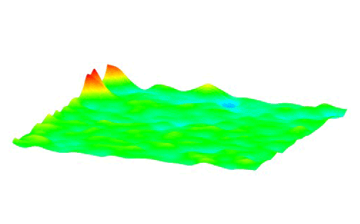
This animation shows how millions of high-voltage switching cycles can cause memristors to fail. The high-voltage switching eventually creates regions that are permanently rich (blue pits) or deficient (red peaks) in oxygen and cannot be switched back. Switching at lower voltages that would be suitable for commercial devices did not show this performance degradation. These observations allowed the researchers to develop materials processing and operating conditions that improved the memristors’ endurance by nearly a thousand times. (Suhas Kumar) Courtesy: SLAC
Here’s a link to and a citation for the paper,
Direct Observation of Localized Radial Oxygen Migration in Functioning Tantalum Oxide Memristors by Suhas Kumar, Catherine E. Graves, John Paul Strachan, Emmanuelle Merced Grafals, Arthur L. David Kilcoyne3, Tolek Tyliszczak, Johanna Nelson Weker, Yoshio Nishi, and R. Stanley Williams. Advanced Materials, First published: 2 February 2016; Print: Volume 28, Issue 14 April 13, 2016 Pages 2772–2776 DOI: 10.1002/adma.201505435
This paper is behind a paywall.
Some of the ‘memristor story’ is contested and you can find a brief overview of the discussion in this Wikipedia memristor entry in the section on ‘definition and criticism’. There is also a history of the memristor which dates back to the 19th century featured in my May 22, 2012 posting.