Tag Archives: James Gimzewski

Physical neural network based on nanowires can learn and remember ‘on the fly’

A November 1, 2023 news item on Nanowerk announced new work on neuromorphic engineering from Australia,

For the first time, a physical neural network has successfully been shown to learn and remember ‘on the fly’, in a way inspired by and similar to how the brain’s neurons work.

The result opens a pathway for developing efficient and low-energy machine intelligence for more complex, real-world learning and memory tasks.

Key Takeaways
*The nanowire-based system can learn and remember ‘on the fly,’ processing dynamic, streaming data for complex learning and memory tasks.

*This advancement overcomes the challenge of heavy memory and energy usage commonly associated with conventional machine learning models.

*The technology achieved a 93.4% accuracy rate in image recognition tasks, using real-time data from the MNIST database of handwritten digits.

*The findings promise a new direction for creating efficient, low-energy machine intelligence applications, such as real-time sensor data processing.

Nanowire neural network
Caption: Electron microscope image of the nanowire neural network that arranges itself like ‘Pick Up Sticks’. The junctions where the nanowires overlap act in a way similar to how our brain’s synapses operate, responding to electric current. Credit: The University of Sydney

A November 1, 2023 University of Sydney news release (also on EurekAlert), which originated the news item, elaborates on the research,

Published today [November 1, 2023] in Nature Communications, the research is a collaboration between scientists at the University of Sydney and University of California at Los Angeles.

Lead author Ruomin Zhu, a PhD student from the University of Sydney Nano Institute and School of Physics, said: “The findings demonstrate how brain-inspired learning and memory functions using nanowire networks can be harnessed to process dynamic, streaming data.”

Nanowire networks are made up of tiny wires that are just billionths of a metre in diameter. The wires arrange themselves into patterns reminiscent of the children’s game ‘Pick Up Sticks’, mimicking neural networks, like those in our brains. These networks can be used to perform specific information processing tasks.

Memory and learning tasks are achieved using simple algorithms that respond to changes in electronic resistance at junctions where the nanowires overlap. Known as ‘resistive memory switching’, this function is created when electrical inputs encounter changes in conductivity, similar to what happens with synapses in our brain.

In this study, researchers used the network to recognise and remember sequences of electrical pulses corresponding to images, inspired by the way the human brain processes information.

Supervising researcher Professor Zdenka Kuncic said the memory task was similar to remembering a phone number. The network was also used to perform a benchmark image recognition task, accessing images in the MNIST database of handwritten digits, a collection of 70,000 small greyscale images used in machine learning.

“Our previous research established the ability of nanowire networks to remember simple tasks. This work has extended these findings by showing tasks can be performed using dynamic data accessed online,” she said.

“This is a significant step forward as achieving an online learning capability is challenging when dealing with large amounts of data that can be continuously changing. A standard approach would be to store data in memory and then train a machine learning model using that stored information. But this would chew up too much energy for widespread application.

“Our novel approach allows the nanowire neural network to learn and remember ‘on the fly’, sample by sample, extracting data online, thus avoiding heavy memory and energy usage.”

Mr Zhu said there were other advantages when processing information online.

“If the data is being streamed continuously, such as it would be from a sensor for instance, machine learning that relied on artificial neural networks would need to have the ability to adapt in real-time, which they are currently not optimised for,” he said.

In this study, the nanowire neural network displayed a benchmark machine learning capability, scoring 93.4 percent in correctly identifying test images. The memory task involved recalling sequences of up to eight digits. For both tasks, data was streamed into the network to demonstrate its capacity for online learning and to show how memory enhances that learning.

Here’s a link to and a citation for the paper,

Online dynamical learning and sequence memory with neuromorphic nanowire networks by Ruomin Zhu, Sam Lilak, Alon Loeffler, Joseph Lizier, Adam Stieg, James Gimzewski & Zdenka Kuncic. Nature Communications volume 14, Article number: 6697 (2023) DOI: https://doi.org/10.1038/s41467-023-42470-5 Published: 01 November 2023

This paper is open access.

You’ll notice a number of this team’s members are also listed in the citation in my June 21, 2023 posting “Learning and remembering like a human brain: nanowire networks” and you’ll see some familiar names in the citation in my June 17, 2020 posting “A tangle of silver nanowires for brain-like action.”

Mechano-photonic artificial synapse is bio-inspired

The word ‘memristor’ usually pops up when there’s research into artificial synapses but not in this new piece of research. I didn’t see any mention of the memristor in the paper’s references either but I did find James Gimzewski from the University of California at Los Angeles (UCLA) whose research into brainlike computing (neuromorphic computing) is running parallel but separately to the memristor research.

Dr. Thamarasee Jeewandara has written a March 25, 2021 article for phys.org about the latest neuromorphic computing research (Note: Links have been removed)

Multifunctional and diverse artificial neural systems can incorporate multimodal plasticity, memory and supervised learning functions to assist neuromorphic computation. In a new report, Jinran Yu and a research team in nanoenergy, nanoscience and materials science in China and the US., presented a bioinspired mechano-photonic artificial synapse with synergistic mechanical and optical plasticity. The team used an optoelectronic transistor made of graphene/molybdenum disulphide (MoS2) heterostructure and an integrated triboelectric nanogenerator to compose the artificial synapse. They controlled the charge transfer/exchange in the heterostructure with triboelectric potential and modulated the optoelectronic synapse behaviors readily, including postsynaptic photocurrents, photosensitivity and photoconductivity. The mechano-photonic artificial synapse is a promising implementation to mimic the complex biological nervous system and promote the development of interactive artificial intelligence. The work is now published on Science Advances.

The human brain can integrate cognition, learning and memory tasks via auditory, visual, olfactory and somatosensory interactions. This process is difficult to be mimicked using conventional von Neumann architectures that require additional sophisticated functions. Brain-inspired neural networks are made of various synaptic devices to transmit information and process using the synaptic weight. Emerging photonic synapse combine the optical and electric neuromorphic modulation and computation to offer a favorable option with high bandwidth, fast speed and low cross-talk to significantly reduce power consumption. Biomechanical motions including touch, eye blinking and arm waving are other ubiquitous triggers or interactive signals to operate electronics during artificial synapse plasticization. In this work, Yu et al. presented a mechano-photonic artificial synapse with synergistic mechanical and optical plasticity. The device contained an optoelectronic transistor and an integrated triboelectric nanogenerator (TENG) in contact-separation mode. The mechano-optical artificial synapses have huge functional potential as interactive optoelectronic interfaces, synthetic retinas and intelligent robots. [emphasis mine]

As you can see Jeewandara has written quite a technical summary of the work. Here’s an image from the Science Advances paper,

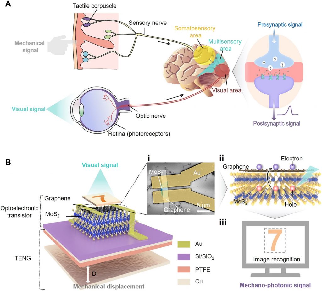
Fig. 1 Biological tactile/visual neurons and mechano-photonic artificial synapse. (A) Schematic illustrations of biological tactile/visual sensory system. (B) Schematic diagram of the mechano-photonic artificial synapse based on graphene/MoS2 (Gr/MoS2) heterostructure. (i) Top-view scanning electron microscope (SEM) image of the optoelectronic transistor; scale bar, 5 μm. The cyan area indicates the MoS2 flake, while the white strip is graphene. (ii) Illustration of charge transfer/exchange for Gr/MoS2 heterostructure. (iii) Output mechano-photonic signals from the artificial synapse for image recognition.

You can find the paper here,

Bioinspired mechano-photonic artificial synapse based on graphene/MoS2 heterostructure by Jinran Yu, Xixi Yang, Guoyun Gao, Yao Xiong, Yifei Wang, Jing Han, Youhui Chen, Huai Zhang, Qijun Sun and Zhong Lin Wang. Science Advances 17 Mar 2021: Vol. 7, no. 12, eabd9117 DOI: 10.1126/sciadv.abd9117

This appears to be open access.

A tangle of silver nanowires for brain-like action

I’ve been meaning to get to this news item from late 2019 as it features work from a team that I’ve been following for a number of years now. First mentioned here in an October 17, 2011 posting, James Gimzewski has been working with researchers at the University of California at Los Angeles (UCLA) and researchers at Japan’s National Institute for Materials Science (NIMS) on neuromorphic computing.

This particular research had a protracted rollout with the paper being published in October 2019 and the last news item about it being published in mid-December 2019.

A December 17, 2029 news item on Nanowerk was the first to alert me to this new work (Note: A link has been removed),

UCLA scientists James Gimzewski and Adam Stieg are part of an international research team that has taken a significant stride toward the goal of creating thinking machines.

Led by researchers at Japan’s National Institute for Materials Science, the team created an experimental device that exhibited characteristics analogous to certain behaviors of the brain — learning, memorization, forgetting, wakefulness and sleep. The paper, published in Scientific Reports (“Emergent dynamics of neuromorphic nanowire networks”), describes a network in a state of continuous flux.

A December 16, 2019 UCLA news release, which originated the news item, offers more detail (Note: A link has been removed),

“This is a system between order and chaos, on the edge of chaos,” said Gimzewski, a UCLA distinguished professor of chemistry and biochemistry, a member of the California NanoSystems Institute at UCLA and a co-author of the study. “The way that the device constantly evolves and shifts mimics the human brain. It can come up with different types of behavior patterns that don’t repeat themselves.”

The research is one early step along a path that could eventually lead to computers that physically and functionally resemble the brain — machines that may be capable of solving problems that contemporary computers struggle with, and that may require much less power than today’s computers do.

The device the researchers studied is made of a tangle of silver nanowires — with an average diameter of just 360 nanometers. (A nanometer is one-billionth of a meter.) The nanowires were coated in an insulating polymer about 1 nanometer thick. Overall, the device itself measured about 10 square millimeters — so small that it would take 25 of them to cover a dime.

Allowed to randomly self-assemble on a silicon wafer, the nanowires formed highly interconnected structures that are remarkably similar to those that form the neocortex, the part of the brain involved with higher functions such as language, perception and cognition.

One trait that differentiates the nanowire network from conventional electronic circuits is that electrons flowing through them cause the physical configuration of the network to change. In the study, electrical current caused silver atoms to migrate from within the polymer coating and form connections where two nanowires overlap. The system had about 10 million of these junctions, which are analogous to the synapses where brain cells connect and communicate.

The researchers attached two electrodes to the brain-like mesh to profile how the network performed. They observed “emergent behavior,” meaning that the network displayed characteristics as a whole that could not be attributed to the individual parts that make it up. This is another trait that makes the network resemble the brain and sets it apart from conventional computers.

After current flowed through the network, the connections between nanowires persisted for as much as one minute in some cases, which resembled the process of learning and memorization in the brain. Other times, the connections shut down abruptly after the charge ended, mimicking the brain’s process of forgetting.

In other experiments, the research team found that with less power flowing in, the device exhibited behavior that corresponds to what neuroscientists see when they use functional MRI scanning to take images of the brain of a sleeping person. With more power, the nanowire network’s behavior corresponded to that of the wakeful brain.

The paper is the latest in a series of publications examining nanowire networks as a brain-inspired system, an area of research that Gimzewski helped pioneer along with Stieg, a UCLA research scientist and an associate director of CNSI.

“Our approach may be useful for generating new types of hardware that are both energy-efficient and capable of processing complex datasets that challenge the limits of modern computers,” said Stieg, a co-author of the study.

The borderline-chaotic activity of the nanowire network resembles not only signaling within the brain but also other natural systems such as weather patterns. That could mean that, with further development, future versions of the device could help model such complex systems.

In other experiments, Gimzewski and Stieg already have coaxed a silver nanowire device to successfully predict statistical trends in Los Angeles traffic patterns based on previous years’ traffic data.

Because of their similarities to the inner workings of the brain, future devices based on nanowire technology could also demonstrate energy efficiency like the brain’s own processing. The human brain operates on power roughly equivalent to what’s used by a 20-watt incandescent bulb. By contrast, computer servers where work-intensive tasks take place — from training for machine learning to executing internet searches — can use the equivalent of many households’ worth of energy, with the attendant carbon footprint.

“In our studies, we have a broader mission than just reprogramming existing computers,” Gimzewski said. “Our vision is a system that will eventually be able to handle tasks that are closer to the way the human being operates.”

The study’s first author, Adrian Diaz-Alvarez, is from the International Center for Material Nanoarchitectonics at Japan’s National Institute for Materials Science. Co-authors include Tomonobu Nakayama and Rintaro Higuchi, also of NIMS; and Zdenka Kuncic at the University of Sydney in Australia.

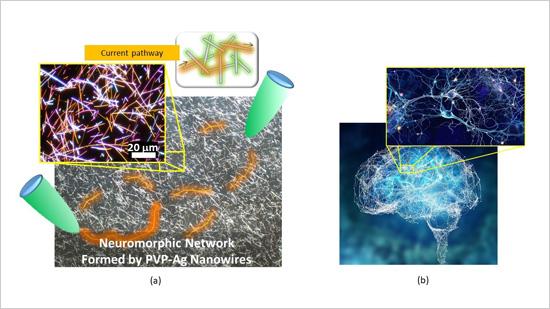
Caption: (a) Micrograph of the neuromorphic network fabricated by this research team. The network contains of numerous junctions between nanowires, which operate as synaptic elements. When voltage is applied to the network (between the green probes), current pathways (orange) are formed in the network. (b) A Human brain and one of its neuronal networks. The brain is known to have a complex network structure and to operate by means of electrical signal propagation across the network. Credit: NIMS

A November 11, 2019 National Institute for Materials Science (Japan) press release (also on EurekAlert but dated December 25, 2019) first announced the news,

An international joint research team led by NIMS succeeded in fabricating a neuromorphic network composed of numerous metallic nanowires. Using this network, the team was able to generate electrical characteristics similar to those associated with higher order brain functions unique to humans, such as memorization, learning, forgetting, becoming alert and returning to calm. The team then clarified the mechanisms that induced these electrical characteristics.

The development of artificial intelligence (AI) techniques has been rapidly advancing in recent years and has begun impacting our lives in various ways. Although AI processes information in a manner similar to the human brain, the mechanisms by which human brains operate are still largely unknown. Fundamental brain components, such as neurons and the junctions between them (synapses), have been studied in detail. However, many questions concerning the brain as a collective whole need to be answered. For example, we still do not fully understand how the brain performs such functions as memorization, learning and forgetting, and how the brain becomes alert and returns to calm. In addition, live brains are difficult to manipulate in experimental research. For these reasons, the brain remains a “mysterious organ.” A different approach to brain research?in which materials and systems capable of performing brain-like functions are created and their mechanisms are investigated?may be effective in identifying new applications of brain-like information processing and advancing brain science.

The joint research team recently built a complex brain-like network by integrating numerous silver (Ag) nanowires coated with a polymer (PVP) insulating layer approximately 1 nanometer in thickness. A junction between two nanowires forms a variable resistive element (i.e., a synaptic element) that behaves like a neuronal synapse. This nanowire network, which contains a large number of intricately interacting synaptic elements, forms a “neuromorphic network”. When a voltage was applied to the neuromorphic network, it appeared to “struggle” to find optimal current pathways (i.e., the most electrically efficient pathways). The research team measured the processes of current pathway formation, retention and deactivation while electric current was flowing through the network and found that these processes always fluctuate as they progress, similar to the human brain’s memorization, learning, and forgetting processes. The observed temporal fluctuations also resemble the processes by which the brain becomes alert or returns to calm. Brain-like functions simulated by the neuromorphic network were found to occur as the huge number of synaptic elements in the network collectively work to optimize current transport, in the other words, as a result of self-organized and emerging dynamic processes..

The research team is currently developing a brain-like memory device using the neuromorphic network material. The team intends to design the memory device to operate using fundamentally different principles than those used in current computers. For example, while computers are currently designed to spend as much time and electricity as necessary in pursuit of absolutely optimum solutions, the new memory device is intended to make a quick decision within particular limits even though the solution generated may not be absolutely optimum. The team also hopes that this research will facilitate understanding of the brain’s information processing mechanisms.

This project was carried out by an international joint research team led by Tomonobu Nakayama (Deputy Director, International Center for Materials Nanoarchitectonics (WPI-MANA), NIMS), Adrian Diaz Alvarez (Postdoctoral Researcher, WPI-MANA, NIMS), Zdenka Kuncic (Professor, School of Physics, University of Sydney, Australia) and James K. Gimzewski (Professor, California NanoSystems Institute, University of California Los Angeles, USA).

Here at last is a link to and a citation for the paper,

Emergent dynamics of neuromorphic nanowire networks by Adrian Diaz-Alvarez, Rintaro Higuchi, Paula Sanz-Leon, Ido Marcus, Yoshitaka Shingaya, Adam Z. Stieg, James K. Gimzewski, Zdenka Kuncic & Tomonobu Nakayama. Scientific Reports volume 9, Article number: 14920 (2019) DOI: https://doi.org/10.1038/s41598-019-51330-6 Published: 17 October 2019

This paper is open access.

Brain-on-a-chip 2014 survey/overview

Michael Berger has written another of his Nanowerk Spotlight articles focussing on neuromorphic engineering and the concept of a brain-on-a-chip bringing it up-to-date April 2014 style.

It’s a topic he and I have been following (separately) for years. Berger’s April 4, 2014 Brain-on-a-chip Spotlight article provides a very welcome overview of the international neuromorphic engineering effort (Note: Links have been removed),

Constructing realistic simulations of the human brain is a key goal of the Human Brain Project, a massive European-led research project that commenced in 2013.

The Human Brain Project is a large-scale, scientific collaborative project, which aims to gather all existing knowledge about the human brain, build multi-scale models of the brain that integrate this knowledge and use these models to simulate the brain on supercomputers. The resulting “virtual brain” offers the prospect of a fundamentally new and improved understanding of the human brain, opening the way for better treatments for brain diseases and for novel, brain-like computing technologies.

Several years ago, another European project named FACETS (Fast Analog Computing with Emergent Transient States) completed an exhaustive study of neurons to find out exactly how they work, how they connect to each other and how the network can ‘learn’ to do new things. One of the outcomes of the project was PyNN, a simulator-independent language for building neuronal network models.

Scientists have great expectations that nanotechnologies will bring them closer to the goal of creating computer systems that can simulate and emulate the brain’s abilities for sensation, perception, action, interaction and cognition while rivaling its low power consumption and compact size – basically a brain-on-a-chip. Already, scientists are working hard on laying the foundations for what is called neuromorphic engineering – a new interdisciplinary discipline that includes nanotechnologies and whose goal is to design artificial neural systems with physical architectures similar to biological nervous systems.

Several research projects funded with millions of dollars are at work with the goal of developing brain-inspired computer architectures or virtual brains: DARPA’s SyNAPSE, the EU’s BrainScaleS (a successor to FACETS), or the Blue Brain project (one of the predecessors of the Human Brain Project) at Switzerland’s EPFL [École Polytechnique Fédérale de Lausanne].

Berger goes on to describe the raison d’être for neuromorphic engineering (attempts to mimic biological brains),

Programmable machines are limited not only by their computational capacity, but also by an architecture requiring (human-derived) algorithms to both describe and process information from their environment. In contrast, biological neural systems (e.g., brains) autonomously process information in complex environments by automatically learning relevant and probabilistically stable features and associations. Since real world systems are always many body problems with infinite combinatorial complexity, neuromorphic electronic machines would be preferable in a host of applications – but useful and practical implementations do not yet exist.

Researchers are mostly interested in emulating neural plasticity (aka synaptic plasticity), from Berger’s April 4, 2014 article,

Independent from military-inspired research like DARPA’s, nanotechnology researchers in France have developed a hybrid nanoparticle-organic transistor that can mimic the main functionalities of a synapse. This organic transistor, based on pentacene and gold nanoparticles and termed NOMFET (Nanoparticle Organic Memory Field-Effect Transistor), has opened the way to new generations of neuro-inspired computers, capable of responding in a manner similar to the nervous system  (read more: “Scientists use nanotechnology to try building computers modeled after the brain”).

One of the key components of any neuromorphic effort, and its starting point, is the design of artificial synapses. Synapses dominate the architecture of the brain and are responsible for massive parallelism, structural plasticity, and robustness of the brain. They are also crucial to biological computations that underlie perception and learning. Therefore, a compact nanoelectronic device emulating the functions and plasticity of biological synapses will be the most important building block of brain-inspired computational systems.

In 2011, a team at Stanford University demonstrates a new single element nanoscale device, based on the successfully commercialized phase change material technology, emulating the functionality and the plasticity of biological synapses. In their work, the Stanford team demonstrated a single element electronic synapse with the capability of both the modulation of the time constant and the realization of the different synaptic plasticity forms while consuming picojoule level energy for its operation (read more: “Brain-inspired computing with nanoelectronic programmable synapses”).

Berger does mention memristors but not in any great detail in this article,

Researchers have also suggested that memristor devices are capable of emulating the biological synapses with properly designed CMOS neuron components. A memristor is a two-terminal electronic device whose conductance can be precisely modulated by charge or flux through it. It has the special property that its resistance can be programmed (resistor) and subsequently remains stored (memory).

One research project already demonstrated that a memristor can connect conventional circuits and support a process that is the basis for memory and learning in biological systems (read more: “Nanotechnology’s road to artificial brains”).

You can find a number of memristor articles here including these: Memristors have always been with us from June 14, 2013; How to use a memristor to create an artificial brain from Feb. 26, 2013; Electrochemistry of memristors in a critique of the 2008 discovery from Sept. 6, 2012; and many more (type ‘memristor’ into the blog search box and you should receive many postings or alternatively, you can try ‘artificial brains’ if you want everything I have on artificial brains).

Getting back to Berger’s April 4, 2014 article, he mentions one more approach and this one stands out,

A completely different – and revolutionary – human brain model has been designed by researchers in Japan who introduced the concept of a new class of computer which does not use any circuit or logic gate. This artificial brain-building project differs from all others in the world. It does not use logic-gate based computing within the framework of Turing. The decision-making protocol is not a logical reduction of decision rather projection of frequency fractal operations in a real space, it is an engineering perspective of Gödel’s incompleteness theorem.

Berger wrote about this work in much more detail in a Feb. 10, 2014 Nanowerk Spotlight article titled: Brain jelly – design and construction of an organic, brain-like computer, (Note: Links have been removed),

In a previous Nanowerk Spotlight we reported on the concept of a full-fledged massively parallel organic computer at the nanoscale that uses extremely low power (“Will brain-like evolutionary circuit lead to intelligent computers?”). In this work, the researchers created a process of circuit evolution similar to the human brain in an organic molecular layer. This was the first time that such a brain-like ‘evolutionary’ circuit had been realized.

The research team, led by Dr. Anirban Bandyopadhyay, a senior researcher at the Advanced Nano Characterization Center at the National Institute of Materials Science (NIMS) in Tsukuba, Japan, has now finalized their human brain model and introduced the concept of a new class of computer which does not use any circuit or logic gate.

In a new open-access paper published online on January 27, 2014, in Information (“Design and Construction of a Brain-Like Computer: A New Class of Frequency-Fractal Computing Using Wireless Communication in a Supramolecular Organic, Inorganic System”), Bandyopadhyay and his team now describe the fundamental computing principle of a frequency fractal brain like computer.

“Our artificial brain-building project differs from all others in the world for several reasons,” Bandyopadhyay explains to Nanowerk. He lists the four major distinctions:
1) We do not use logic gate based computing within the framework of Turing, our decision-making protocol is not a logical reduction of decision rather projection of frequency fractal operations in a real space, it is an engineering perspective of Gödel’s incompleteness theorem.
2) We do not need to write any software, the argument and basic phase transition for decision-making, ‘if-then’ arguments and the transformation of one set of arguments into another self-assemble and expand spontaneously, the system holds an astronomically large number of ‘if’ arguments and its associative ‘then’ situations.
3) We use ‘spontaneous reply back’, via wireless communication using a unique resonance band coupling mode, not conventional antenna-receiver model, since fractal based non-radiative power management is used, the power expense is negligible.
4) We have carried out our own single DNA, single protein molecule and single brain microtubule neurophysiological study to develop our own Human brain model.

I encourage people to read Berger’s articles on this topic as they provide excellent information and links to much more. Curiously (mind you, it is easy to miss something), he does not mention James Gimzewski’s work at the University of California at Los Angeles (UCLA). Working with colleagues from the National Institute for Materials Science in Japan, Gimzewski published a paper about “two-, three-terminal WO3-x-based nanoionic devices capable of a broad range of neuromorphic and electrical functions”. You can find out more about the paper in my Dec. 24, 2012 posting titled: Synaptic electronics.

As for the ‘brain jelly’ paper, here’s a link to and a citation for it,

Design and Construction of a Brain-Like Computer: A New Class of Frequency-Fractal Computing Using Wireless Communication in a Supramolecular Organic, Inorganic System by Subrata Ghoshemail, Krishna Aswaniemail, Surabhi Singhemail, Satyajit Sahuemail, Daisuke Fujitaemail and Anirban Bandyopadhyay. Information 2014, 5(1), 28-100; doi:10.3390/info5010028

It’s an open access paper.

As for anyone who’s curious about why the US BRAIN initiative ((Brain Research through Advancing Innovative Neurotechnologies, also referred to as the Brain Activity Map Project) is not mentioned, I believe that’s because it’s focussed on biological brains exclusively at this point (you can check its Wikipedia entry to confirm).

Anirban Bandyopadhyay was last mentioned here in a January 16, 2014 posting titled: Controversial theory of consciousness confirmed (maybe) in  the context of a presentation in Amsterdam, Netherlands.
Getting neuromorphic with a synaptic transistor

Scientists at Harvard University (Massachusetts, US) have devised a transistor that simulates the synapses found in brains. From a Nov. 2, 2013 news item on ScienceDaily,

It doesn’t take a Watson to realize that even the world’s best supercomputers are staggeringly inefficient and energy-intensive machines.

Our brains have upwards of 86 billion neurons, connected by synapses that not only complete myriad logic circuits; they continuously adapt to stimuli, strengthening some connections while weakening others. We call that process learning, and it enables the kind of rapid, highly efficient computational processes that put Siri and Blue Gene to shame.

Materials scientists at the Harvard School of Engineering and Applied Sciences (SEAS) have now created a new type of transistor that mimics the behavior of a synapse. The novel device simultaneously modulates the flow of information in a circuit and physically adapts to changing signals.

Exploiting unusual properties in modern materials, the synaptic transistor could mark the beginning of a new kind of artificial intelligence: one embedded not in smart algorithms but in the very architecture of a computer. [emphasis mine]

There are two other projects that I know of (and I imagine there are others) focused on intelligence that’s embedded rather than algorithmic. My December 24, 2012 posting focused on a joint (National Institute for Materials Science in Japan and the University of California, Los Angeles) project where researchers developed a nanoionic device with a range of neuromorphic and electrical properties. There’s also the memristor mentioned in my Feb. 26, 2013 posting (and many other times on this blog) which features a ,proposal to create an artificial brain.

Getting back to Harvard’s synaptic transistor (from the Nov. 1, 2013 Harvard University news release which originated the news item),

The human mind, for all its phenomenal computing power, runs on roughly 20 Watts of energy (less than a household light bulb), so it offers a natural model for engineers.

“The transistor we’ve demonstrated is really an analog to the synapse in our brains,” says co-lead author Jian Shi, a postdoctoral fellow at SEAS. “Each time a neuron initiates an action and another neuron reacts, the synapse between them increases the strength of its connection. And the faster the neurons spike each time, the stronger the synaptic connection. Essentially, it memorizes the action between the neurons.”

In principle, a system integrating millions of tiny synaptic transistors and neuron terminals could take parallel computing into a new era of ultra-efficient high performance.

Here’s an image of synaptic transistors that the researchers from Harvard’s School of Engineering and Applied Science (SEAS) have supplied,

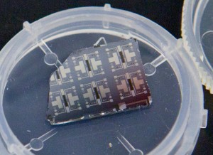
Several prototypes of the synaptic transistor are visible on this silicon chip. (Photo by Eliza Grinnell, SEAS Communications.)

Several prototypes of the synaptic transistor are visible on this silicon chip. (Photo by Eliza Grinnell, SEAS Communications.)

The news release provides a description of the synatpic transistor and how it works,

While calcium ions and receptors effect a change in a biological synapse, the artificial version achieves the same plasticity with oxygen ions. When a voltage is applied, these ions slip in and out of the crystal lattice of a very thin (80-nanometer) film of samarium nickelate, which acts as the synapse channel between two platinum “axon” and “dendrite” terminals. The varying concentration of ions in the nickelate raises or lowers its conductance—that is, its ability to carry information on an electrical current—and, just as in a natural synapse, the strength of the connection depends on the time delay in the electrical signal.

Structurally, the device consists of the nickelate semiconductor sandwiched between two platinum electrodes and adjacent to a small pocket of ionic liquid. An external circuit multiplexer converts the time delay into a magnitude of voltage which it applies to the ionic liquid, creating an electric field that either drives ions into the nickelate or removes them. The entire device, just a few hundred microns long, is embedded in a silicon chip.

The synaptic transistor offers several immediate advantages over traditional silicon transistors. For a start, it is not restricted to the binary system of ones and zeros.

“This system changes its conductance in an analog way, continuously, as the composition of the material changes,” explains Shi. “It would be rather challenging to use CMOS, the traditional circuit technology, to imitate a synapse, because real biological synapses have a practically unlimited number of possible states—not just ‘on’ or ‘off.’”

The synaptic transistor offers another advantage: non-volatile memory, which means even when power is interrupted, the device remembers its state.

Additionally, the new transistor is inherently energy efficient. The nickelate belongs to an unusual class of materials, called correlated electron systems, that can undergo an insulator-metal transition. At a certain temperature—or, in this case, when exposed to an external field—the conductance of the material suddenly changes.

“We exploit the extreme sensitivity of this material,” says Ramanathan [principal investigator and associate professor of materials science at Harvard SEAS]. “A very small excitation allows you to get a large signal, so the input energy required to drive this switching is potentially very small. That could translate into a large boost for energy efficiency.”

The nickelate system is also well positioned for seamless integration into existing silicon-based systems.

“In this paper, we demonstrate high-temperature operation, but the beauty of this type of a device is that the ‘learning’ behavior is more or less temperature insensitive, and that’s a big advantage,” says Ramanathan. “We can operate this anywhere from about room temperature up to at least 160 degrees Celsius.”

For now, the limitations relate to the challenges of synthesizing a relatively unexplored material system, and to the size of the device, which affects its speed.

“In our proof-of-concept device, the time constant is really set by our experimental geometry,” says Ramanathan. “In other words, to really make a super-fast device, all you’d have to do is confine the liquid and position the gate electrode closer to it.”

In fact, Ramanathan and his research team are already planning, with microfluidics experts at SEAS, to investigate the possibilities and limits for this “ultimate fluidic transistor.”

Here’s a link to and a citation for the researchers’ paper,

A correlated nickelate synaptic transistor by Jian Shi, Sieu D. Ha, You Zhou, Frank Schoofs, & Shriram Ramanathan. Nature Communications 4, Article number: 2676 doi:10.1038/ncomms3676 Published 31 October 2013

This article is behind a paywall.

MORPHONANO, an art/sci exhibit in California

This description of the event (MORPHONANO) which is being held at the Beall Center at the University of California (Irvine) comes from the Beall Center’s home page,

MORPHONANO explores a number of art works created by media artist Victoria Vesna and nanoscientist James Gimzewski. Their collaborative works create an intersection of space, time and embodiment by employing a very subtle and responsive energetic exchange. Participants interact with the works in mindful ways resulting in rich visual and sonic experiences within a meditative space. By reversing the scale of nanotechnology to the realm of human experience, the artist and scientist create a sublime reversal of space-time.

Here’s an image depicting one of the exhibits in the show,

ZERO@WAVEFUNCTION plays with the idea of scale and molecular manipulation from a distance with the participant changing the structures of the buckyballs with their shadows, a real time interactive metaphor of the scanning tunneling microscope (STM).

It looks to me that the idea is to ’embody’ the nanoscale as per the caption “the participants changing the structures of the buckyballs with their shadows, a real time interactive metaphor of the scanning tunneling microscope.” There’s a larger version of the image and information about this exhibit in the Feb. 14, 2012 news item on Nanowerk,

BLUE MORPH is an interactive installation that uses nanoscale images combined with sounds derived from the microscopic undulations of a chrysalis during the period of its metamorphosis into a butterfly recorded using nanotechnology. The work is designed to be responsive to minute, subtle, mindful movements of the participant creating a rich visual and sonic experience of morphing. Most is revealed in complete stillness.

NANOMANDALA is a video projected onto a disk of sand, 8 feet in diameter. Visitors can touch the sand as images are projected in evolving scale from the molecular structure of a single grain of sand – achieved my means of photography, optical and scanning electron microscopy (SEM) – to the recognizable image of the complete mandala, and then back again. The original Chakrasamvara mandala was created by monks of the Ghaden Lhopa Khangsten monastery. Patience will allow experiencing the whole.

ZERO@WAVEFUNCTION plays with the idea of scale and molecular manipulation from a distance with the participant changing the structures of the buckyballs with their shadows, a real time interactive metaphor of the scanning tunneling microscope (STM). Slow motion makes change happen.

BRAIN STORMING: SOUNDS OF THINKING a premier of a work of self organization in progress focusing on scale invariant and the brain using biometric data. A number of brain storming sessions with cutting neuroscientists, nanotechnologists, philosophers and monks will take place throughout the exhibition. In many ways the works in this exhibition reverse the scale of nanotechnology to a visible realm and time in nano scale creating a sublime reversal of space-time.

The show opened Feb. 2 and closes May 6, 2012. The address is

Beall Center for Art + Technology
University of California, Irvine
Claire Trevor School of the Arts
712 Arts Plaza
Irvine, CA 92697-2775
www.beallcenter.uci.edu

Here are some details about the art/sci collaborators, Victoria Vesna and James Gimzewski, from the undated Beall Center news release,

Victoria Vesna is a media artist and Professor at the Department of Design | Media Arts at the UCLA School of the Arts and director of the UCLA Art|Sci center. Currently she is Visiting Professor at Art, Media + Technology, Parsons the New School for Design in New York and a senior researcher at IMéRA – Institut Méditerranéen de Recherches Avancées in Marseille, France. Her work can be defined as experimental creative research that resides between disciplines and technologies. She explores how communication technologies affect collective behavior and how perceptions of identity shift in relation to scientific innovation. Her most recent experiential installations — Blue Morph, Water Bowls, Hox Zodiac, all aim to raise consciousness around environmental issues natural and human-animal relations. …

James Gimzewski FRS is a distinguished Professor in the Dept. of Chemistry and Biochemistry at UCLA. He is director of Pico and Nano core laboratory at the California NanoSynstems Institute (CNSI). He is also scientific director of the Art | Sci center and a senior fellow of IMéRA. He is a satellite co-director and PI of materials nanoarchitectonics at the National Institute of Material Science in Tsukuba, Japan. Until February 2001, he was a group leader at the IBM Zurich Labs, where he was involved in Nanoscale science since 1983. He pioneered research on electrical contact with single atoms and molecules, light emission and molecular imaging using STM. His accomplishments include the first STM-manipulation of molecules at room temperature, the realization of molecular abacus using buckyballs, the discovery of single molecule rotors and the development of nanomechanical sensors based on nanotechnology, which explore the ultimate limits of sensitivity and measurement. …

I have mentioned Gimzewski previously in a post (Oct. 17, 2011) about a three-part nanotechnology series on Canadian television.