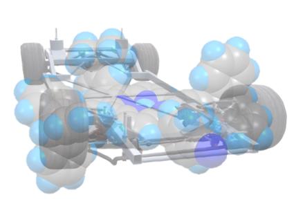
Caption: Chemical structure of the nanocar qualified. Credit: G. Rapenne, NAIST and UPS
That’s pretty nifty, superimposing a chemical structure over an image of either a real race car or a toy. A June 16, 2020 Nara Institute of Science and Technology press release (also on EurekAlert but published on June 15, 2020) announces preparations for the next nano Grand Prix in 2021 but first there’s a little history,
According to the British Royal Automobile and the French Automobile clubs, the first car was created in 1770 by the Frenchman Joseph Cugnot. This “Fardier” (French name for a trolley used to transport heavy loads) was a car propelled by a steam engine and powered by a boiler. This 7 m long self-propelled machine reached a speed of 4 km/h, for an average autonomy of 15 min. 250 years later, researchers at the Nara Institute of Science and Technology (NAIST), Japan, in partnership with colleagues in the University Paul Sabatier (Toulouse, France), report in Chemistry – A European Journal a new family of nanocars integrating a dipole to speed up their motion in the nanoworld.
After the first nanocar race organized in spring 2017, in Toulouse (France) we designed a new family of molecules to behave as cars in the nanoworld. When I established my laboratory in NAIST in April 2018, Toshio Nishino (Assistant Professor) and Hiroki Takeuchi (Master student) started the synthesis. Two years later, we are reporting the results in a publication presenting the synthesis of 9 dipolar nanocars. The result is amazing. In every flask, about 100 mg of green or blue powders (i.e. 60 x 1018 nanocars) stick to the walls. These are the Franco-Japanese racing cars that sleep wisely in the garage waiting for the next Grand Prix in 2021.
“To hope to win the race, nanocars have to be fast but they need also to be controllable,” emphasizes Gwénaël Rapenne. The design of the molecules has long been thought to need a compromise between opposite requirements. Consistently, the nanocar Rapenne and his colleagues designed is made up of 150 atoms (chemical formula C85H59N5Zn). A planar chassis made from porphyrin, a fragment already used in nature for many processes like oxygen transportation (hemoglobin) or photosynthesis (chlorophyl). Ultimately, the presence of a zinc atom could allow transportation of small molecules on the car body. “The nanocar is 2 nm long and surrounded by four wheels designed to minimize contact with the ground and has two legs which are able to donate or accept electrons making the nanocar dipolar” specifies the researcher.
What kind of application could be envisioned with such small vehicles?
“Honestly, today, we do not know yet what this technology will be used for. But just like the liquid crystals discovered in 1910 and not used until half a century later in calculator screens and now in all our LCD supports, the manipulation of molecules could well be revolutionary, ” dreams Gwénaël Rapenne. One of the directions of the research could be to carry a load to transport reactants or drugs from one place to another.
Here’s a link to and a citation for the paper,
Dipolar Nanocars Based on a Porphyrin Backbone by Toshio Nishino, Colin J. Martin, Hiroki Takeuchi, Florence Lim, Kazuma Yasuhara, Yohan Gisbert, Seifallah Abid, Nathalie Saffon-Merceron, Claire Kammerer, Gwénaël Rapenne. Chemistry Europe DOI: https://doi.org/10.1002/chem.202001999 First published: 12 June 2020
This paper is behind a paywall.
For anyone curious about the 2017 race, I found this May 9, 2017 posting, which notes that a US-Austrian team won.
I always appreciate a reference to Star Trek and three-dimensional chess was one of my favourite concepts. You’ll find that and more in a May 19, 2020 news item on Nanowerk,
Researchers at The Institute of Scientific and Industrial Research at Osaka University [Japan] introduced a new liquid-phase fabrication method for producing nanocellulose films with multiple axes of alignment. Using 3D-printing methods for increased control, this work may lead to cheaper and more environmentally friendly optical and thermal devices.
Ever since appearing on the original Star Trek TV show in the 1960s, the game of “three-dimensional chess” has been used as a metaphor for sophisticated thinking. Now, researchers at Osaka University can say that they have added their own version, with potential applications in advanced optics and inexpensive smartphone displays.
It’s not exactly three-dimensional chess but this nanocellulose film was produced by 3D printing methods,
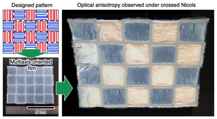
Caption: Developed multiaxis nanocellulose-oriented film. Credit: Osaka University
Many existing optical devices, including liquid-crystal displays (LCDs) found in older flat-screen televisions, rely on long needle-shaped molecules aligned in the same direction. However, getting fibers to line up in multiple directions on the same device is much more difficult. Having a method that can reliably and cheaply produce optical fibers would accelerate the manufacture of low-cost displays or even “paper electronics”–computers that could be printed from biodegradable materials on demand.
Cellulose, the primary component of cotton and wood, is an abundant renewable resource made of long molecules. Nanocelluloses are nanofibers made of uniaxially aligned cellulose molecular chains that have different optical and heat conduction properties along one direction compared to the another.
In newly published research from the Institute of Scientific and Industrial Research at Osaka University, nanocellulose was harvested from sea pineapples, a kind of sea squirt. They then used liquid-phase 3D-pattering, which combined the wet spinning of nanofibers with the precision of 3D-printing. A custom-made triaxial robot dispensed a nanocellulose aqueous suspension into an acetone coagulation bath.
“We developed this liquid-phase three-dimensional patterning technique to allow for nanocellulose alignment along any preferred axis,” says first author Kojiro Uetani. The direction of the patterns could be programmed so that it formed an alternating checkerboard pattern of vertically- and horizontally-aligned fibers.
To demonstrate the method, a film was sandwiched between two orthogonal polarizing films. Under the proper viewing conditions, a birefringent checkerboard pattern appeared. They also measured the thermal transfer and optical retardation properties.
“Our findings could aid in the development of next-generation optical materials and paper electronics,” says senior author Masaya Nogi. “This could be the start of bottom-up techniques for building sophisticated and energy-efficient optical and thermal materials.”
I’ve been meaning to get to this news item from late 2019 as it features work from a team that I’ve been following for a number of years now. First mentioned here in an October 17, 2011 posting, James Gimzewski has been working with researchers at the University of California at Los Angeles (UCLA) and researchers at Japan’s National Institute for Materials Science (NIMS) on neuromorphic computing.
This particular research had a protracted rollout with the paper being published in October 2019 and the last news item about it being published in mid-December 2019.
A December 17, 2029 news item on Nanowerk was the first to alert me to this new work (Note: A link has been removed),
UCLA scientists James Gimzewski and Adam Stieg are part of an international research team that has taken a significant stride toward the goal of creating thinking machines.
Led by researchers at Japan’s National Institute for Materials Science, the team created an experimental device that exhibited characteristics analogous to certain behaviors of the brain — learning, memorization, forgetting, wakefulness and sleep. The paper, published in Scientific Reports (“Emergent dynamics of neuromorphic nanowire networks”), describes a network in a state of continuous flux.
“This is a system between order and chaos, on the edge of chaos,” said Gimzewski, a UCLA distinguished professor of chemistry and biochemistry, a member of the California NanoSystems Institute at UCLA and a co-author of the study. “The way that the device constantly evolves and shifts mimics the human brain. It can come up with different types of behavior patterns that don’t repeat themselves.”
The research is one early step along a path that could eventually lead to computers that physically and functionally resemble the brain — machines that may be capable of solving problems that contemporary computers struggle with, and that may require much less power than today’s computers do.
The device the researchers studied is made of a tangle of silver nanowires — with an average diameter of just 360 nanometers. (A nanometer is one-billionth of a meter.) The nanowires were coated in an insulating polymer about 1 nanometer thick. Overall, the device itself measured about 10 square millimeters — so small that it would take 25 of them to cover a dime.
Allowed to randomly self-assemble on a silicon wafer, the nanowires formed highly interconnected structures that are remarkably similar to those that form the neocortex, the part of the brain involved with higher functions such as language, perception and cognition.
One trait that differentiates the nanowire network from conventional electronic circuits is that electrons flowing through them cause the physical configuration of the network to change. In the study, electrical current caused silver atoms to migrate from within the polymer coating and form connections where two nanowires overlap. The system had about 10 million of these junctions, which are analogous to the synapses where brain cells connect and communicate.
The researchers attached two electrodes to the brain-like mesh to profile how the network performed. They observed “emergent behavior,” meaning that the network displayed characteristics as a whole that could not be attributed to the individual parts that make it up. This is another trait that makes the network resemble the brain and sets it apart from conventional computers.
After current flowed through the network, the connections between nanowires persisted for as much as one minute in some cases, which resembled the process of learning and memorization in the brain. Other times, the connections shut down abruptly after the charge ended, mimicking the brain’s process of forgetting.
In other experiments, the research team found that with less power flowing in, the device exhibited behavior that corresponds to what neuroscientists see when they use functional MRI scanning to take images of the brain of a sleeping person. With more power, the nanowire network’s behavior corresponded to that of the wakeful brain.
The paper is the latest in a series of publications examining nanowire networks as a brain-inspired system, an area of research that Gimzewski helped pioneer along with Stieg, a UCLA research scientist and an associate director of CNSI.
“Our approach may be useful for generating new types of hardware that are both energy-efficient and capable of processing complex datasets that challenge the limits of modern computers,” said Stieg, a co-author of the study.
The borderline-chaotic activity of the nanowire network resembles not only signaling within the brain but also other natural systems such as weather patterns. That could mean that, with further development, future versions of the device could help model such complex systems.
In other experiments, Gimzewski and Stieg already have coaxed a silver nanowire device to successfully predict statistical trends in Los Angeles traffic patterns based on previous years’ traffic data.
Because of their similarities to the inner workings of the brain, future devices based on nanowire technology could also demonstrate energy efficiency like the brain’s own processing. The human brain operates on power roughly equivalent to what’s used by a 20-watt incandescent bulb. By contrast, computer servers where work-intensive tasks take place — from training for machine learning to executing internet searches — can use the equivalent of many households’ worth of energy, with the attendant carbon footprint.
“In our studies, we have a broader mission than just reprogramming existing computers,” Gimzewski said. “Our vision is a system that will eventually be able to handle tasks that are closer to the way the human being operates.”
The study’s first author, Adrian Diaz-Alvarez, is from the International Center for Material Nanoarchitectonics at Japan’s National Institute for Materials Science. Co-authors include Tomonobu Nakayama and Rintaro Higuchi, also of NIMS; and Zdenka Kuncic at the University of Sydney in Australia.
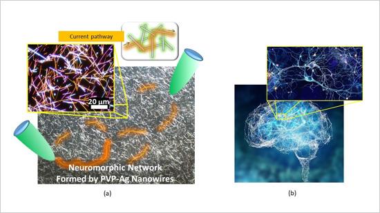
Caption: (a) Micrograph of the neuromorphic network fabricated by this research team. The network contains of numerous junctions between nanowires, which operate as synaptic elements. When voltage is applied to the network (between the green probes), current pathways (orange) are formed in the network. (b) A Human brain and one of its neuronal networks. The brain is known to have a complex network structure and to operate by means of electrical signal propagation across the network. Credit: NIMS
An international joint research team led by NIMS succeeded in fabricating a neuromorphic network composed of numerous metallic nanowires. Using this network, the team was able to generate electrical characteristics similar to those associated with higher order brain functions unique to humans, such as memorization, learning, forgetting, becoming alert and returning to calm. The team then clarified the mechanisms that induced these electrical characteristics.
The development of artificial intelligence (AI) techniques has been rapidly advancing in recent years and has begun impacting our lives in various ways. Although AI processes information in a manner similar to the human brain, the mechanisms by which human brains operate are still largely unknown. Fundamental brain components, such as neurons and the junctions between them (synapses), have been studied in detail. However, many questions concerning the brain as a collective whole need to be answered. For example, we still do not fully understand how the brain performs such functions as memorization, learning and forgetting, and how the brain becomes alert and returns to calm. In addition, live brains are difficult to manipulate in experimental research. For these reasons, the brain remains a “mysterious organ.” A different approach to brain research?in which materials and systems capable of performing brain-like functions are created and their mechanisms are investigated?may be effective in identifying new applications of brain-like information processing and advancing brain science.
The joint research team recently built a complex brain-like network by integrating numerous silver (Ag) nanowires coated with a polymer (PVP) insulating layer approximately 1 nanometer in thickness. A junction between two nanowires forms a variable resistive element (i.e., a synaptic element) that behaves like a neuronal synapse. This nanowire network, which contains a large number of intricately interacting synaptic elements, forms a “neuromorphic network”. When a voltage was applied to the neuromorphic network, it appeared to “struggle” to find optimal current pathways (i.e., the most electrically efficient pathways). The research team measured the processes of current pathway formation, retention and deactivation while electric current was flowing through the network and found that these processes always fluctuate as they progress, similar to the human brain’s memorization, learning, and forgetting processes. The observed temporal fluctuations also resemble the processes by which the brain becomes alert or returns to calm. Brain-like functions simulated by the neuromorphic network were found to occur as the huge number of synaptic elements in the network collectively work to optimize current transport, in the other words, as a result of self-organized and emerging dynamic processes..
The research team is currently developing a brain-like memory device using the neuromorphic network material. The team intends to design the memory device to operate using fundamentally different principles than those used in current computers. For example, while computers are currently designed to spend as much time and electricity as necessary in pursuit of absolutely optimum solutions, the new memory device is intended to make a quick decision within particular limits even though the solution generated may not be absolutely optimum. The team also hopes that this research will facilitate understanding of the brain’s information processing mechanisms.
This project was carried out by an international joint research team led by Tomonobu Nakayama (Deputy Director, International Center for Materials Nanoarchitectonics (WPI-MANA), NIMS), Adrian Diaz Alvarez (Postdoctoral Researcher, WPI-MANA, NIMS), Zdenka Kuncic (Professor, School of Physics, University of Sydney, Australia) and James K. Gimzewski (Professor, California NanoSystems Institute, University of California Los Angeles, USA).
Here at last is a link to and a citation for the paper,
Emergent dynamics of neuromorphic nanowire networks by Adrian Diaz-Alvarez, Rintaro Higuchi, Paula Sanz-Leon, Ido Marcus, Yoshitaka Shingaya, Adam Z. Stieg, James K. Gimzewski, Zdenka Kuncic & Tomonobu Nakayama. Scientific Reports volume 9, Article number: 14920 (2019) DOI: https://doi.org/10.1038/s41598-019-51330-6 Published: 17 October 2019
A new, cheaper method easily and effectively separates two types of carbon nanotubes. The process, developed by Nagoya University researchers in Japan, could be up-scaled for manufacturing purified batches of single-wall carbon nanotubes that can be used in high-performance electronic devices.
Single-wall carbon nanotubes (SWCNTs) have excellent electronic and mechanical properties, making them ideal candidates for use in a wide range of electronic devices, including the thin-film transistors found in LCD displays. A problem is that only two-thirds of manufactured SWCNTs are suitable for use in electronic devices. The useful semiconducting SWCNTs must be separated from the unwanted metallic ones. But the most powerful purification process, known as aqueous two-phase extraction, currently involves the use of a costly polysaccharide, called dextran.
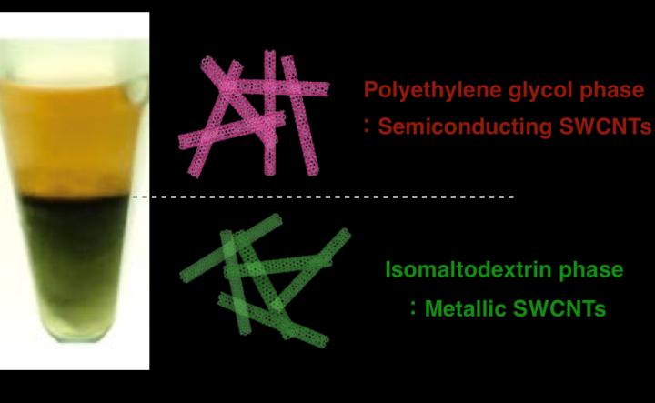
Caption: The unwanted metallic SWCNTs deposited at the bottom of the solution, while the wanted semiconducting ones floated to the top. Credit: Haruka Omachi
Organic chemist Haruka Omachi and colleagues at Nagoya University hypothesized that dextran’s effectiveness in separating semiconducting from metallic SWCNTs lies in the linkages connecting its glucose units. Instead of using dextran to separate the two types of SWCNTs, the team tried the significantly cheaper isomaltodextran, which has many more of these linkages.
A batch of SWCNTs was left for 15 minutes in a solution containing polyethylene glycol and isomaltodextrin and then centrifuged for five minutes. Three different types of isomaltodextrin were tried, each with a different number of linkages and a different molecular weight. The team found that metallic SWCNTs separated to the bottom isomaltodextrin part of the solution, while the semiconducting SWCNTs floated to the top polyethylene glycol part.
The type of isomaltodextrin with high molecular weight and the most linkages was the most (99%) effective in separating the two types of SWCNTs. The team also found that another polysaccharide, called pullulan, whose glucose units are connected with different kinds of linkages, was ineffective in separating the two types of SWCNTs. The researchers suggest that the number and type of linkages present in isomaltodextrin play an important role in their ability to effectively separate the carbon nanotubes.
The team also found that a thin-film transistor made with their purified semiconducting SWCNTs performed very well.
Isomaltodextrin is a cheap and widely available polysaccharide produced from starch that is used as a dietary fibre. This makes it a cost-effective alternative for the SWCNT extraction process. Omachi and his colleagues are currently in discussions with companies to commercialize their approach. They are also working on improving the performance of thin-film transistors using semiconducting SWCNTs in flexible displays and sensor devices.
[downloaded from https://sp.spiber.jp/en/tnfsp/mp/]
Adele Peters in her October 31, 2019 article for Fast Company describes the technology used to make this jacket,
A typical waterproof winter jacket is made with nylon—a material that, like other plastics, is made from petroleum. But a new limited-edition jacket from The North Face Japan uses something called “brewed protein” instead. It’s a material inspired by spider silk that is fermented in giant vats, the same way that breweries make beer.
It’s one of the first uses of a material produced by the Japanese startup Spiber, a company that has spent more than a decade developing a new process to make high-performance textiles and other products that don’t rely on fossil fuels, animals, or natural fibers like cotton, all of which have environmental issues. …
The company designs genes that code for a specific protein—the first was an exact replica of natural spider silk, known for its extreme strength—and then introduces the genes into microorganisms that can produce the protein efficiently. Inside giant tanks, the microorganisms are fed sugar, grow and multiply, and produce the protein through fermentation. …
Spiber first started collaborating with Goldwin, a Japanese outdoor brand that owns the Japanese rights to The North Face, in 2015, and created an early prototype of a jacket then. But it quickly realized that an exact replica of spider silk wouldn’t work well for the application; the material sucks up water, and the jacket needed to be waterproof.
“We spent the last four years going back to the drawing board, redesigning our protein molecule—the very order of the amino acids in the molecule,” says Meyer [Daniel Meyer, Spiber’s head of corporate global marketing]. “And we created our own hydrophobic [water repellent] version of spider silk. It’s inspired by natural spider silk, but we have made our own design changes such that it would be more hydrophobic and meet the performance requirements of The North Face Japan.”
…
The jacket is available for purchase but only by a lottery, which has now closed. According to Peters, a large, commercial production facility is being built in Thailand so that at some point a Moon Parka will be affordable. For reference, the lottery jackets were priced at ¥150,000 (about $1,377 US).
You can find Spiber here in mid-March [2020] according to the homepage.
Weaving a quantum processor from light is a jaw-dropping event (as far as I’m concerned). An October 17, 2019 news item on phys.org makes the announcement,
An international team of scientists from Australia, Japan and the United States has produced a prototype of a large-scale quantum processor made of laser light.
Based on a design ten years in the making, the processor has built-in scalability that allows the number of quantum components—made out of light—to scale to extreme numbers. The research was published in Science today [October 18, 2019; Note: I cannot explain the discrepancy between the dates]].
Quantum computers promise fast solutions to hard problems, but to do this they require a large number of quantum components and must be relatively error free. Current quantum processors are still small and prone to errors. This new design provides an alternative solution, using light, to reach the scale required to eventually outperform classical computers on important problems.
…
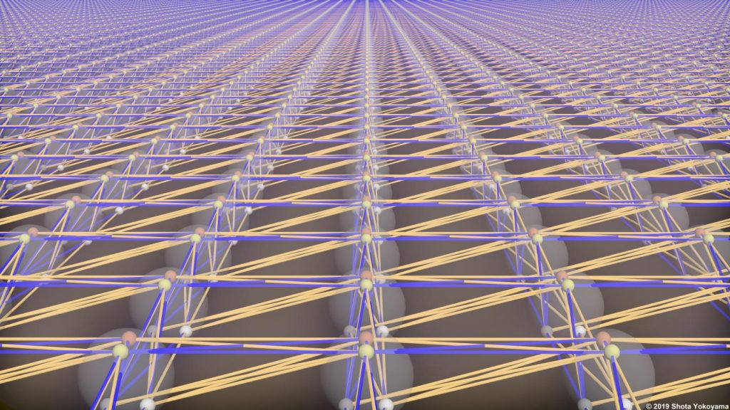
Caption: The entanglement structure of a large-scale quantum processor made of light. Credit: Shota Yokoyama 2019
“While today’s quantum processors are impressive, it isn’t clear if the current designs can be scaled up to extremely large sizes,” notes Dr Nicolas Menicucci, Chief Investigator at the Centre for Quantum Computation and Communication Technology (CQC2T) at RMIT University in Melbourne, Australia.
“Our approach starts with extreme scalability – built in from the very beginning – because the processor, called a cluster state, is made out of light.”
Using light as a quantum processor
A cluster state is a large collection of entangled quantum components that performs quantum computations when measured in a particular way.
“To be useful for real-world problems, a cluster state must be both large enough and have the right entanglement structure. In the two decades since they were proposed, all previous demonstrations of cluster states have failed on one or both of these counts,” says Dr Menicucci. “Ours is the first ever to succeed at both.”
To make the cluster state, specially designed crystals convert ordinary laser light into a type of quantum light called squeezed light, which is then weaved into a cluster state by a network of mirrors, beamsplitters and optical fibres.
The team’s design allows for a relatively small experiment to generate an immense two-dimensional cluster state with scalability built in. Although the levels of squeezing – a measure of quality – are currently too low for solving practical problems, the design is compatible with approaches to achieve state-of-the-art squeezing levels.
The team says their achievement opens up new possibilities for quantum computing with light.
“In this work, for the first time in any system, we have made a large-scale cluster state whose structure enables universal quantum computation.” Says Dr Hidehiro Yonezawa, Chief Investigator, CQC2T at UNSW Canberra. “Our experiment demonstrates that this design is feasible – and scalable.”
###
The experiment was an international effort, with the design developed through collaboration by Dr Menicucci at RMIT, Dr Rafael Alexander from the University of New Mexico and UNSW Canberra researchers Dr Hidehiro Yonezawa and Dr Shota Yokoyama. A team of experimentalists at the University of Tokyo, led by Professor Akira Furusawa, performed the ground-breaking experiment.
Here’s a link to and a citation for the paper,
Generation of time-domain-multiplexed two-dimensional cluster state by Warit Asavanant, Yu Shiozawa, Shota Yokoyama, Baramee Charoensombutamon, Hiroki Emura, Rafael N. Alexander, Shuntaro Takeda, Jun-ichi Yoshikawa, Nicolas C. Menicucci, Hidehiro Yonezawa, Akira Furusawa. Science 18 Oct 2019: Vol. 366, Issue 6463, pp. 373-376 DOI: 10.1126/science.aay2645
If you’re hoping for gold flecks in your glue, this is not going to satisfy you, given that it’s all at the nanoscale. An August 7, 2019 news item on Nanowerk briefly describes this gold glue (Note: A link has been removed),
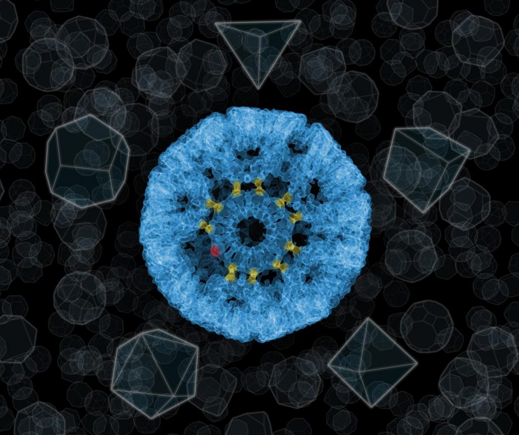
It has long been known that gold can be used to do things that philosophers have never even dreamed of. The Institute of Nuclear Physics of the Polish Academy of Sciences in Cracow has confirmed the existence of ‘gold glue’: bonds involving gold atoms, capable of permanently bonding protein rings. Skilfully used by an international team of scientists, the bonds have made it possible to construct molecular nanocages with a structure so far unparalleled in nature or even in mathematics (Nature, “An ultra-stable gold-coordinated protein cage displaying reversible assembly”).
Caption: The ‘impossible’ sphere, i.e. a molecular nanocage of 24 protein rings, each of which has an 11-sided structure. The rings are connected by bonds with the participation of gold atoms, here marked in yellow. Depending on their position in the structure, not all gold atoms have to be used to attach adjacent proteins (an unused gold atom is marked in red).
Credit: Source: UJ, IFJ PAN
The world of science has been interested in molecular cages for years. Not without reason. Chemical molecules, including those that would under normal conditions enter into chemical reactions, can be enclosed within their empty interiors. The particles of the enclosed compound, separated by the walls of the cage from the environment, have nothing to bond with. These cages can be therefore be used, for example, to transport drugs safely into a cancer cell, only releasing the drug when they are inside it.
Molecular cages are polyhedra made up of smaller ‘bricks’, usually protein molecules. The bricks can’t be of any shape. For example, if we wanted to build a molecular polyhedron using only objects with the outline of an equilateral triangle, geometry would limit us to only three solid figures: a tetrahedron, an octahedron or an icosahedron. So far, there have been no other structural possibilities.
“Fortunately, Platonic idealism is not a dogma of the physical world. If you accept certain inaccuracies in the solid figure being constructed, you can create structures with shapes that are not found in nature, what’s more, with very interesting properties,” says Dr. Tomasz Wrobel from the Cracow Institute of Nuclear Physics of the Polish Academy of Sciences (IFJ PAN).
Dr. Wrobel is one of the members of an international team of researchers who have recently carried out the ‘impossible’: they built a cage similar in shape to a sphere out of eleven-walled proteins. The main authors of this spectacular success are scientists from the group of Prof. Jonathan Heddle from the Malopolska Biotechnology Centre of the Jagiellonian University in Cracow and the Japanese RIKEN Institute in Wako. The work described in Nature magazine took place with the participation of researchers from universities in Osaka and Tsukuba (Japan), Durham (Great Britain), Waterloo (Canada) and other research centres.
Each of the walls of the new nanocages was formed by a protein ring from which eleven cysteine molecules stuck out at regular intervals. It was to the sulphur atom found in each cysteine molecule that the ‘glue’, i.e. the gold atom, was planned to be attached. In the appropriate conditions, it could bind with one more sulphur atom, in the cysteine of a next ring. In this way a permanent chemical bond would be formed between the two rings. But would the gold atom under these conditions really be able to form a bond between the rings?
“In the Spectroscopic Imaging Laboratory of IFJ PAS we used Raman spectroscopy and X-ray photoelectron spectroscopy to show that in the samples provided to us with the test nanocages, the gold really did form bonds with sulphur atoms in cysteines. In other words, in a difficult, direct measurement, we proved that gold ‘glue’ for bonding protein rings in cages really does exist,” explains Dr. Wrobel.
Each gold atom can be treated as a stand-alone clip that makes it possible to attach another ring. The road to the ‘impossible’ begins when we realize that we don’t always have to use all of the clips! So, although all the rings of the new nanocages are physically the same, depending on their place in the structure they connect with their neighbours with a different number of gold atoms, and thus function as polygons with different numbers of vertices. 24 nanocage walls presented by the researchers were held together by 120 gold atoms. The outer diameter of the cages was 22 nanometres and the inner diameter was 16 nm.
Using gold atoms as a binder for nanocages is also important due to its possible applications. In earlier molecular structures, proteins were glued together using many weak chemical bonds. The complexity of the bonds and their similarity to the bonds responsible for the existence of the protein rings themselves did not allow for precise control over the decomposition of the cages. This is not the case in the new structures. On the one hand, gold-bonded nanocages are chemically and thermally stable (for example, they withstand hours of boiling in water). On the other hand, however, gold bonds are sensitive to an increase in acidity. By its increase, the nanocage can be decomposed in a controlled way and the contents can be released into the environment. Since the acidity within cells is greater than outside them, gold-bonded nanocages are ideal for biomedical applications.
The ‘impossible’ nanocage is the presentation of a qualitatively new approach to the construction of molecular cages, with gold atoms in the role of loose clips. The demonstrated flexibility of the gold bonds will make it possible in the future to create nanocages with sizes and features precisely tailored to specific needs.
Here’s a link to and a citation for the paper.
An ultra-stable gold-coordinated protein cage displaying reversible assembly by Ali D. Malay, Naoyuki Miyazaki, Artur Biela, Soumyananda Chakraborti, Karolina Majsterkiewicz, Izabela Stupka, Craig S. Kaplan, Agnieszka Kowalczyk, Bernard M. A. G. Piette, Georg K. A. Hochberg, Di Wu, Tomasz P. Wrobel, Adam Fineberg, Manish S. Kushwah, Mitja Kelemen, Primož Vavpetič, Primož Pelicon, Philipp Kukura, Justin L. P. Benesch, Kenji Iwasaki & Jonathan G. Heddle Nature volume 569, pages438–442 (2019) Issue Date: 16 May 2019 DOI: https://doi.org/10.1038/s41586-019-1185-4 Published online: 08 May 2019
A July 19, 2019 news item on phys.org describes research that may result in a substantive change for information technology,
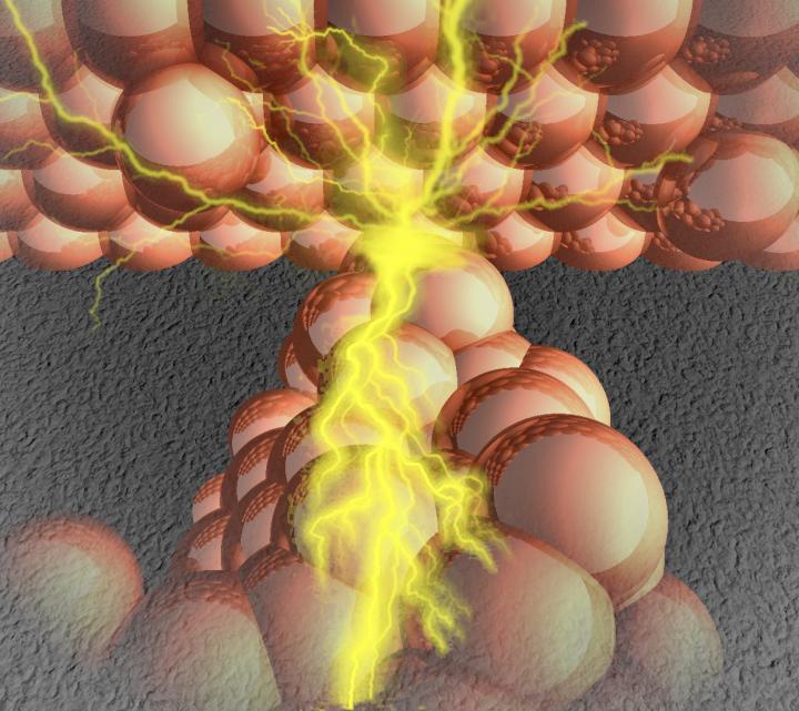
A team of researchers from Tokyo Institute of Technology has gained unprecedented insight into the inner workings of an atomic switch. By investigating the composition of the tiny metal ‘bridge’ that forms inside the switch, their findings may spur the design of atomic switches with improved performance.
Atomic switches are hailed as the tiniest of electrochemical switches that could change the face of information technology. Due to their nanoscale dimensions and low power consumption, they hold promise for integration into next-generation circuits that could drive the development of artificial intelligence (AI) and Internet of Things (IoT) devices.
Although various designs have emerged, one intriguing question concerns the nature of the metallic filament, or bridge, that is key to the operation of the switch. The bridge forms inside a metal sulfide layer sandwiched between two electrodes [see figure below], and is controlled by applying a voltage that induces an electrochemical reaction. The formation and annihilation of this bridge determines whether the switch is on or off.
Now, a research group including Akira Aiba and Manabu Kiguchi and colleagues at Tokyo Institute of Technology’s Department of Chemistry has found a useful way to examine precisely what the bridge is composed of.
By cooling the atomic switch enough so as to be able to investigate the bridge using a low-temperature measurement technique called point contact spectroscopy (PCS) [2], their study revealed that the bridge is made up of metal atoms from both the electrode and the metal sulfide layer. This surprising finding controverts the prevailing notion that the bridge derives from the electrode only, Kiguchi explains.
The team compared atomic switches with different combinations of electrodes (Pt and Ag, or Pt and Cu) and metal sulfide layers (Cu2S and Ag2S). In both cases, they found that the bridge is mainly composed of Ag.
The reason behind the dominance of Ag in the bridge is likely due to “the higher mobility of Ag ions compared to Cu ions”, the researchers say in their paper published in ACS Applied Materials & Interfaces.
They conclude that “it would be better to use metals with low mobility” for designing atomic switches with higher stability.
Much remains to be explored in the advancement of atomic switch technologies, and the team is continuing to investigate which combination of elements would be the most effective in improving performance.
###
Technical terms [1] Atomic switch: The idea behind an atomic switch — one that can be controlled by the motion of a single atom — was introduced by Donald Eigler and colleagues at the IBM Almaden Research Center in 1991. Interest has since focused on how to realize and harness the potential of such extremely small switches for use in logic circuits and memory devices. Over the past two decades, researchers in Japan have taken a world-leading role in the development of atomic switch technologies. [2] Point contact spectroscopy: A method of measuring the properties or excitations of single atoms at low temperature.
Caption: The ‘bridge’ that forms within the metal sulfide layer, connecting two metal electrodes, results in the atomic switch being turned on. Credit: Manabu Kiguchi
For anyone who might need a bit of a refresher for the chemical elements, Pt is platinum, Ag is silver, and Cu is copper. So, with regard to the metal sulfide layers Cu2S is copper sulfide and Ag2S is silver sulfide.
A June 17,2019 news item on phys.org describes a new technique for producing nanoparticles,
One of the major challenges in nanotechnology is the precise control of shape, size and elemental composition of every single nanoparticle. Physical methods are able to produce homogeneous nanoparticles free of surface contamination. However, they offer limited opportunity to control the shape and specific composition of the nanoobjects when they are being built up.
A recent collaboration between the University of Helsinki and the Okinawa Institute of Science and Technology (OIST) Graduate University revealed that hybrid Au/Fe nanoparticles can grow in an unprecedentedly complex structure with a single-step fabrication method. Using a computational modeling framework, the groups of Professor Flyura Djurabekova at the University of Helsinki and Prof. Sowwan at OIST succeeded in deciphering the growth mechanism by a detailed multistage model.
Elegantly combined considerations of kinetic and thermodynamic effects explained the formation of embedded gold layers and the site-specific surface gold decoration. These results open up a possibility for engineering a multitude of hybrid nanoparticles for a wide range of emerging applications. Their research was recently published in the highly ranked open access journal Advanced Science.
“When nature surprises us with an unexpectedly beautiful pattern, we must recognize it and explain. This is the way to cooperate with nature that is always ready to teach and expecting us to learn,” says Dr. Junlei Zhao, a postdoctoral researcher in the group of Prof. Djurabekova.
Nowadays, scientists are able to study nano-scale phenomena with great accuracy by using high-performance computational software and modern supercomputing infrastructures. These are of great support, not only for advancing fundamental science but also for finding promising solutions for many challenges of humanity.
Here’s a link to and a citation for the paper,
Site‐Specific Wetting of Iron Nanocubes by Gold Atoms in Gas‐Phase Synthesis by Jerome Vernieres, Stephan Steinhauer, Junlei Zhao, Panagiotis Grammatikopoulos, Riccardo Ferrando, Kai Nordlund, Flyura Djurabekova, Mukhles Sowwan. Advanced Science Volume 6, Issue 13 1900447 uly 3, 2019 DOI: https://doi.org/10.1002/advs.201900447 First published online: 02 May 2019
I don’t know the dates for the last ‘golden’ age of electronics but I can certainly understand why these Japanese researchers are excited about their work. In any event, I think the ‘golden age’ is more of a play on words. From a June 25, 2019 news item on Nanowerk (Note: A link has been removed),
One way that heat damages electronic equipment is it makes components expand at different rates, resulting in forces that cause micro-cracking and distortion. Plastic components and circuit boards are particularly prone to damage due to changes in volume during heating and cooling cycles. But if a material could be incorporated into the components that compensates for the expansion, the stresses would be reduced and their lifetime increased.
Everybody knows one material that behaves like this: liquid water expands when it freezes and ice contracts when it melts. But liquid water and electronics don’t mix well – instead, what’s needed is a solid with “negative thermal expansion” (NTE).
Although such materials have been known since the 1960s, a number of challenges had to be overcome before the concept would be broadly useful and commercially viable. In terms of both materials and function, these efforts have only had limited success.
The experimental materials had been produced under specialized laboratory conditions using expensive equipment; and even then, the temperature and pressure ranges in which they would exhibit NTE were well outside normal everyday conditions.
Moreover, the amount they expanded and contracted depended on the direction, which induced internal stresses that changed their structure, meaning that the NTE property would not last longer than a few heating and cooling cycles.
A research team led by Koshi Takenaka of Nagoya University has succeeded in overcoming these materials-engineering challenges (APL Materials, “Valence fluctuations and giant isotropic negative thermal expansion in Sm1–xRxS (R = Y, La, Ce, Pr, Nd)”).
Inspired by the series of work by Noriaki Sato, also of Nagoya University – whose discovery last year of superconductivity in quasicrystals was considered one of the top ten physics discoveries of the year by Physics World magazine – Professor Takenaka took the rare earth element samarium and its sulfide, samarium monosulfide (SmS), which is known to change phase from the “black phase” to the smaller-volume “golden phase”. The problem was to tune the range of temperatures at which the phase transition occurs. The team’s solution was to replace a small proportion of samarium atoms with another rare earth element, giving Sm1-xRxS, where “R” is any one of the rare earth elements cerium (Ce), neodymium (Nd), praseodymium (Pr) or yttrium (Y). The fraction x the team used was typically 0.2, except for yttrium. These materials showed “giant negative thermal expansion” of up to 8% at ordinary room pressure and a useful range of temperatures (around 150 degrees) including at room temperature and above … . Cerium is the star candidate here because it is relatively cheap.
The nature of the phase transition is such that the materials can be powdered into very small crystal sizes around a micron on a side without losing their negative expansion property. This broadens the industrial applications, particularly within electronics.
While the Nagoya University group’s engineering achievement is impressive, how the negative expansion works is fascinating from a fundamental physics viewpoint. During the black-golden transition, the crystal structure stays the same but the atoms get closer together: the unit cell size becomes smaller because (as is very likely but perhaps not yet 100% certain) the electron structure of the samarium atoms changes and makes them smaller – a process of intra-atomic charge transfer called a “valence transition” or “valence fluctuation” within the samarium atoms … . “My impression,” says Professor Takenaka, “is that the correlation between the lattice volume and the electron structure of samarium is experimentally verified for this class of sulfides.”
More specifically, in the black (lower temperature) phase, the electron configuration of the samarium atoms is (4f)6, meaning that in their outermost shell they have 6 electrons in the f orbitals (with s, p and d orbitals filled); while in the golden phase the electronic configuration is (4f)5(5d)1 -an electron has moved out of a 4f orbital into a 5d orbital. Although a “higher” shell is starting to be occupied, it turns out – through a quirk of the Pauli Exclusion Principle – that the second case gives a smaller atom size, leading to a smaller crystal size and negative expansion.
But this is only part of the fundamental picture. In the black phase, samarium sulfide and its doped offshoots are insulators – they do not conduct electricity; while in the golden phase they turn into conductors (i.e. metals). This is suggesting that during the black-golden phase transition the band structure of the whole crystal is influencing the valance transition within the samarium atoms. Although nobody has done the theoretical calculations for the doped samarium sulfides made by Professor Takenaka’s group, a previous theoretical study has indicated that when electrons leave the samarium atoms’ f orbital, they leave behind a positively charged “hole” which itself interacts repulsively with holes in the crystal’s conduction band, affecting their exchange interaction. This becomes a cooperative effect that then drives the valence transition in the samarium atoms. The exact mechanism, though, is not well understood.
Nevertheless, the Nagoya University-led group’s achievement is one of engineering, not pure physics. “What is important for many engineers is the ability to use the material to reduce device failure due to thermal expansion,” explains Professor Takenaka. “In short, in a certain temperature range – the temperature range in which the intended device operates, typically an interval of dozens of degrees or more – the volume needs to gradually decrease with a rise in temperature and increase as the temperature falls. Of course, I also know that volume expansion on cooling during a phase transition [like water freezing] is a common case for many materials. However, if the volume changes in a very narrow temperature range, there is no engineering value. The present achievement is the result of material engineering, not pure physics.”
Perhaps it even heralds a new “golden” age for electronics.
I worked in a company for a data communications company that produced hardware and network management software. From a hardware perspective, heat was an enemy which distorted your circuit boards and cost you significant money not only for replacements but also when you included fans to keep the equipment cool (or as cool as possible).
Enough with the reminiscences, here’s a link to and a citation for the paper,