Tag Archives: Jia Liu

Cyborg organoids?

Every time I think I’ve become inured to the idea of a fuzzy boundary between life and nonlife something new crosses my path such as integrating nanoelectronics with cells for cyborg organoids. An August 9, 2019 news item on ScienceDaily makes the announcement,

What happens in the early days of organ development? How do a small group of cells organize to become a heart, a brain, or a kidney? This critical period of development has long remained the black box of developmental biology, in part because no sensor was small or flexible enough to observe this process without damaging the cells.

Now, researchers from the Harvard John A. Paulson School of Engineering and Applied Sciences (SEAS) have grown simplified organs known as organoids with fully integrated sensors. These so-called cyborg organoids offer a rare glimpse into the early stages of organ development.

An August 8, 2019 Harvard John A. Paulson School of Engineering and Applied Sciences news release (also on EurekAlert but published August 9, 2019) by Leah Burrows, which originated the news item, expands on the theme,

“I was so inspired by the natural organ development process in high school, in which 3D organs start from few cells in 2D structures. I think if we can develop nanoelectronics that are so flexible, stretchable, and soft that they can grow together with developing tissue through their natural development process, the embedded sensors can measure the entire activity of this developmental process,” said Jia Liu, Assistant Professor of Bioengineering at SEAS and senior author of the study. “The end result is a piece of tissue with a nanoscale device completely distributed and integrated across the entire three-dimensional volume of the tissue.”

This type of device emerges from the work that Liu began as a graduate student in the lab of Charles M. Lieber, the Joshua and Beth Friedman University Professor. In Lieber’s lab, Liu once developed flexible, mesh-like nanoelectronics that could be injected in specific regions of tissue.

Building on that design, Liu and his team increased the stretchability of the nanoelectronics by changing the shape of the mesh from straight lines to serpentine structures (similar structures are used in wearable electronics). Then, the team transferred the mesh nanoelectronics onto a 2D sheet of stem cells, where the cells covered and interwove with the nanoelectronics via cell-cell attraction forces. As the stem cells began to morph into a 3D structure, the nanoelectronics seamlessly reconfigured themselves along with the cells, resulting in fully-grown 3D organoids with embedded sensors.

The stem cells were then differentiated into cardiomyocytes — heart cells — and the researchers were able to monitor and record the electrophysiological activity for 90 days.

“This method allows us to continuously monitor the developmental process and understand how the dynamics of individual cells start to interact and synchronize during the entire developmental process,” said Liu. “It could be used to turn any organoid into cyborg organoids, including brain and pancreas organoids.”

In addition to helping answer fundamental questions about biology, cyborg organoids could be used to test and monitor patient-specific drug treatments and potentially used for transplantations.

Here’s a link to and a citation for the paper

Cyborg Organoids: Implantation of Nanoelectronics via Organogenesis for Tissue-Wide Electrophysiology by Qiang Li, Kewang Nan, Paul Le Floch, Zuwan Lin, Hao Sheng, Thomas S. Blum, Jia Liu. Nano Lett.20191985781-5789 DOI: https://doi.org/10.1021/acs.nanolett.9b02512 Publication Date:July 26, 2019 Copyright © 2019 American Chemical Society

This paper is behind a paywall.

Gamechanging electronics with new ultrafast, flexible, and transparent electronics

There are two news bits about game-changing electronics, one from the UK and the other from the US.

United Kingdom (UK)

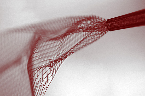
An April 3, 2017 news item on Azonano announces the possibility of a future golden age of electronics courtesy of the University of Exeter,

Engineering experts from the University of Exeter have come up with a breakthrough way to create the smallest, quickest, highest-capacity memories for transparent and flexible applications that could lead to a future golden age of electronics.

A March 31, 2017 University of Exeter press release (also on EurekAlert), which originated the news item, expands on the theme (Note: Links have been removed),

Engineering experts from the University of Exeter have developed innovative new memory using a hybrid of graphene oxide and titanium oxide. Their devices are low cost and eco-friendly to produce, are also perfectly suited for use in flexible electronic devices such as ‘bendable’ mobile phone, computer and television screens, and even ‘intelligent’ clothing.

Crucially, these devices may also have the potential to offer a cheaper and more adaptable alternative to ‘flash memory’, which is currently used in many common devices such as memory cards, graphics cards and USB computer drives.

The research team insist that these innovative new devices have the potential to revolutionise not only how data is stored, but also take flexible electronics to a new age in terms of speed, efficiency and power.

Professor David Wright, an Electronic Engineering expert from the University of Exeter and lead author of the paper said: “Using graphene oxide to produce memory devices has been reported before, but they were typically very large, slow, and aimed at the ‘cheap and cheerful’ end of the electronics goods market.

“Our hybrid graphene oxide-titanium oxide memory is, in contrast, just 50 nanometres long and 8 nanometres thick and can be written to and read from in less than five nanoseconds – with one nanometre being one billionth of a metre and one nanosecond a billionth of a second.”

Professor Craciun, a co-author of the work, added: “Being able to improve data storage is the backbone of tomorrow’s knowledge economy, as well as industry on a global scale. Our work offers the opportunity to completely transform graphene-oxide memory technology, and the potential and possibilities it offers.”

Here’s a link to and a citation for the paper,

Multilevel Ultrafast Flexible Nanoscale Nonvolatile Hybrid Graphene Oxide–Titanium Oxide Memories by V. Karthik Nagareddy, Matthew D. Barnes, Federico Zipoli, Khue T. Lai, Arseny M. Alexeev, Monica Felicia Craciun, and C. David Wright. ACS Nano, 2017, 11 (3), pp 3010–3021 DOI: 10.1021/acsnano.6b08668 Publication Date (Web): February 21, 2017

Copyright © 2017 American Chemical Society

This paper appears to be open access.

United States (US)

Researchers from Stanford University have developed flexible, biodegradable electronics.

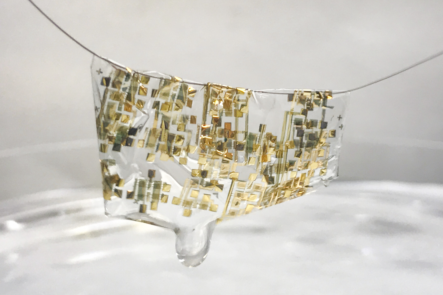
A newly developed flexible, biodegradable semiconductor developed by Stanford engineers shown on a human hair. (Image credit: Bao lab)

A human hair? That’s amazing and this May 3, 2017 news item on Nanowerk reveals more,

As electronics become increasingly pervasive in our lives – from smart phones to wearable sensors – so too does the ever rising amount of electronic waste they create. A United Nations Environment Program report found that almost 50 million tons of electronic waste were thrown out in 2017–more than 20 percent higher than waste in 2015.

Troubled by this mounting waste, Stanford engineer Zhenan Bao and her team are rethinking electronics. “In my group, we have been trying to mimic the function of human skin to think about how to develop future electronic devices,” Bao said. She described how skin is stretchable, self-healable and also biodegradable – an attractive list of characteristics for electronics. “We have achieved the first two [flexible and self-healing], so the biodegradability was something we wanted to tackle.”

The team created a flexible electronic device that can easily degrade just by adding a weak acid like vinegar. The results were published in the Proceedings of the National Academy of Sciences (“Biocompatible and totally disintegrable semiconducting polymer for ultrathin and ultralightweight transient electronics”).

“This is the first example of a semiconductive polymer that can decompose,” said lead author Ting Lei, a postdoctoral fellow working with Bao.

A May 1, 2017 Stanford University news release by Sarah Derouin, which originated the news item, provides more detail,

In addition to the polymer – essentially a flexible, conductive plastic – the team developed a degradable electronic circuit and a new biodegradable substrate material for mounting the electrical components. This substrate supports the electrical components, flexing and molding to rough and smooth surfaces alike. When the electronic device is no longer needed, the whole thing can biodegrade into nontoxic components.

Biodegradable bits

Bao, a professor of chemical engineering and materials science and engineering, had previously created a stretchable electrode modeled on human skin. That material could bend and twist in a way that could allow it to interface with the skin or brain, but it couldn’t degrade. That limited its application for implantable devices and – important to Bao – contributed to waste.

Flexible, biodegradable semiconductor on an avacado

The flexible semiconductor can adhere to smooth or rough surfaces and biodegrade to nontoxic products. (Image credit: Bao lab)

Bao said that creating a robust material that is both a good electrical conductor and biodegradable was a challenge, considering traditional polymer chemistry. “We have been trying to think how we can achieve both great electronic property but also have the biodegradability,” Bao said.

Eventually, the team found that by tweaking the chemical structure of the flexible material it would break apart under mild stressors. “We came up with an idea of making these molecules using a special type of chemical linkage that can retain the ability for the electron to smoothly transport along the molecule,” Bao said. “But also this chemical bond is sensitive to weak acid – even weaker than pure vinegar.” The result was a material that could carry an electronic signal but break down without requiring extreme measures.

In addition to the biodegradable polymer, the team developed a new type of electrical component and a substrate material that attaches to the entire electronic component. Electronic components are usually made of gold. But for this device, the researchers crafted components from iron. Bao noted that iron is a very environmentally friendly product and is nontoxic to humans.

The researchers created the substrate, which carries the electronic circuit and the polymer, from cellulose. Cellulose is the same substance that makes up paper. But unlike paper, the team altered cellulose fibers so the “paper” is transparent and flexible, while still breaking down easily. The thin film substrate allows the electronics to be worn on the skin or even implanted inside the body.

From implants to plants

The combination of a biodegradable conductive polymer and substrate makes the electronic device useful in a plethora of settings – from wearable electronics to large-scale environmental surveys with sensor dusts.

“We envision these soft patches that are very thin and conformable to the skin that can measure blood pressure, glucose value, sweat content,” Bao said. A person could wear a specifically designed patch for a day or week, then download the data. According to Bao, this short-term use of disposable electronics seems a perfect fit for a degradable, flexible design.

And it’s not just for skin surveys: the biodegradable substrate, polymers and iron electrodes make the entire component compatible with insertion into the human body. The polymer breaks down to product concentrations much lower than the published acceptable levels found in drinking water. Although the polymer was found to be biocompatible, Bao said that more studies would need to be done before implants are a regular occurrence.

Biodegradable electronics have the potential to go far beyond collecting heart disease and glucose data. These components could be used in places where surveys cover large areas in remote locations. Lei described a research scenario where biodegradable electronics are dropped by airplane over a forest to survey the landscape. “It’s a very large area and very hard for people to spread the sensors,” he said. “Also, if you spread the sensors, it’s very hard to gather them back. You don’t want to contaminate the environment so we need something that can be decomposed.” Instead of plastic littering the forest floor, the sensors would biodegrade away.

As the number of electronics increase, biodegradability will become more important. Lei is excited by their advancements and wants to keep improving performance of biodegradable electronics. “We currently have computers and cell phones and we generate millions and billions of cell phones, and it’s hard to decompose,” he said. “We hope we can develop some materials that can be decomposed so there is less waste.”

Other authors on the study include Ming Guan, Jia Liu, Hung-Cheng Lin, Raphael Pfattner, Leo Shaw, Allister McGuire, and Jeffrey Tok of Stanford University; Tsung-Ching Huang of Hewlett Packard Enterprise; and Lei-Lai Shao and Kwang-Ting Cheng of University of California, Santa Barbara.

The research was funded by the Air Force Office for Scientific Research; BASF; Marie Curie Cofund; Beatriu de Pinós fellowship; and the Kodak Graduate Fellowship.

Here’s a link to and a citation for the team’s latest paper,

Biocompatible and totally disintegrable semiconducting polymer for ultrathin and ultralightweight transient electronics by Ting Lei, Ming Guan, Jia Liu, Hung-Cheng Lin, Raphael Pfattner, Leo Shaw, Allister F. McGuire, Tsung-Ching Huang, Leilai Shao, Kwang-Ting Cheng, Jeffrey B.-H. Tok, and Zhenan Bao. PNAS 2017 doi: 10.1073/pnas.1701478114 published ahead of print May 1, 2017

This paper is behind a paywall.

The mention of cellulose in the second item piqued my interest so I checked to see if they’d used nanocellulose. No, they did not. Microcrystalline cellulose powder was used to constitute a cellulose film but they found a way to render this film at the nanoscale. From the Stanford paper (Note: Links have been removed),

… Moreover, cellulose films have been previously used as biodegradable substrates in electronics (28⇓–30). However, these cellulose films are typically made with thicknesses well over 10 μm and thus cannot be used to fabricate ultrathin electronics with substrate thicknesses below 1–2 μm (7, 18, 19). To the best of our knowledge, there have been no reports on ultrathin (1–2 μm) biodegradable substrates for electronics. Thus, to realize them, we subsequently developed a method described herein to obtain ultrathin (800 nm) cellulose films (Fig. 1B and SI Appendix, Fig. S8). First, microcrystalline cellulose powders were dissolved in LiCl/N,N-dimethylacetamide (DMAc) and reacted with hexamethyldisilazane (HMDS) (31, 32), providing trimethylsilyl-functionalized cellulose (TMSC) (Fig. 1B). To fabricate films or devices, TMSC in chlorobenzene (CB) (70 mg/mL) was spin-coated on a thin dextran sacrificial layer. The TMSC film was measured to be 1.2 μm. After hydrolyzing the film in 95% acetic acid vapor for 2 h, the trimethylsilyl groups were removed, giving a 400-nm-thick cellulose film. The film thickness significantly decreased to one-third of the original film thickness, largely due to the removal of the bulky trimethylsilyl groups. The hydrolyzed cellulose film is insoluble in most organic solvents, for example, toluene, THF, chloroform, CB, and water. Thus, we can sequentially repeat the above steps to obtain an 800-nm-thick film, which is robust enough for further device fabrication and peel-off. By soaking the device in water, the dextran layer is dissolved, starting from the edges of the device to the center. This process ultimately releases the ultrathin substrate and leaves it floating on water surface (Fig. 3A, Inset).

Finally, I don’t have any grand thoughts; it’s just interesting to see different approaches to flexible electronics.

‘Bionic’ cardiac patch with nanoelectric scaffolds and living cells

A June 27, 2016 news item on Nanowerk announced that Harvard University researchers may have taken us a step closer to bionic cardiac patches for human hearts (Note: A link has been removed),

Scientists and doctors in recent decades have made vast leaps in the treatment of cardiac problems – particularly with the development in recent years of so-called “cardiac patches,” swaths of engineered heart tissue that can replace heart muscle damaged during a heart attack.

Thanks to the work of Charles Lieber and others, the next leap may be in sight.

The Mark Hyman, Jr. Professor of Chemistry and Chair of the Department of Chemistry and Chemical Biology, Lieber, postdoctoral fellow Xiaochuan Dai and other co-authors of a study that describes the construction of nanoscale electronic scaffolds that can be seeded with cardiac cells to produce a “bionic” cardiac patch. The study is described in a June 27 [2016] paper published in Nature Nanotechnology (“Three-dimensional mapping and regulation of action potential propagation in nanoelectronics-innervated tissues”).

A June 27, 2016 Harvard University press release on EurekAlert, which originated the news item, provides more information,

“I think one of the biggest impacts would ultimately be in the area that involves replaced of damaged cardiac tissue with pre-formed tissue patches,” Lieber said. “Rather than simply implanting an engineered patch built on a passive scaffold, our works suggests it will be possible to surgically implant an innervated patch that would now be able to monitor and subtly adjust its performance.”

Once implanted, Lieber said, the bionic patch could act similarly to a pacemaker – delivering electrical shocks to correct arrhythmia, but the possibilities don’t end there.

“In this study, we’ve shown we can change the frequency and direction of signal propagation,” he continued. “We believe it could be very important for controlling arrhythmia and other cardiac conditions.”

Unlike traditional pacemakers, Lieber said, the bionic patch – because its electronic components are integrated throughout the tissue – can detect arrhythmia far sooner, and operate at far lower voltages.

“Even before a person started to go into large-scale arrhythmia that frequently causes irreversible damage or other heart problems, this could detect the early-stage instabilities and intervene sooner,” he said. “It can also continuously monitor the feedback from the tissue and actively respond.”

“And a normal pacemaker, because it’s on the surface, has to use relatively high voltages,” Lieber added.

The patch might also find use, Lieber said, as a tool to monitor the responses under cardiac drugs, or to help pharmaceutical companies to screen the effectiveness of drugs under development.

Likewise, the bionic cardiac patch can also be a unique platform, he further mentioned, to study the tissue behavior evolving during some developmental processes, such as aging, ischemia or differentiation of stem cells into mature cardiac cells.

Although the bionic cardiac patch has not yet been implanted in animals, “we are interested in identifying collaborators already investigating cardiac patch implantation to treat myocardial infarction in a rodent model,” he said. “I don’t think it would be difficult to build this into a simpler, easily implantable system.”

In the long term, Lieber believes, the development of nanoscale tissue scaffolds represents a new paradigm for integrating biology with electronics in a virtually seamless way.

Using the injectable electronics technology he pioneered last year, Lieber even suggested that similar cardiac patches might one day simply be delivered by injection.

“It may actually be that, in the future, this won’t be done with a surgical patch,” he said. “We could simply do a co-injection of cells with the mesh, and it assembles itself inside the body, so it’s less invasive.”

Here’s a link to and a citation for the paper,

Three-dimensional mapping and regulation of action potential propagation in nanoelectronics-innervated tissues by Xiaochuan Dai, Wei Zhou, Teng Gao, Jia Liu & Charles M. Lieber. Nature Nanotechnology (2016)  doi:10.1038/nnano.2016.96 Published online 27 June 2016

This paper is behind a paywall.

Dexter Johnson in a June 27, 2016 posting on his Nanoclast blog (on the IEEE [Institute of Electrical and Electronics Engineers] website) provides more technical detail (Note: Links have been removed),

In research described in the journal Nature Nanotechnology, Lieber and his team employed a bottom-up approach that started with the fabrication of doped p-type silicon nanowires. Lieber has been spearheading the use of silicon nanowires as a scaffold for growing nerve, heart, and muscle tissue for years now.

In this latest work, Lieber and his team fabricated the nanowires, applied them onto a polymer surface, and arranged them into a field-effect transistor (FET). The researchers avoided an increase in the device’s impedance as its dimensions were reduced by adopting this FET approach as opposed to simply configuring the device as an electrode. Each FET, along with its source-drain interconnects, created a 4-micrometer-by-20-micrometer-by-350-nanometer pad. Each of these pads was, in effect, a single recording device.

I recommend reading Dexter’s posting in its entirety as Charles Lieber shares additional technical information not found in the news release.

No more kevlar-wrapped lithium-ion batteries?

Current lithium-ion batteries present a fire hazard, which is why, last, year a team of researchers at the University of Michigan came up with a plan to prevent fires by wrapping the batteries in kevlar. My Jan. 30, 2015 post describes the research and provides some information about airplane fires caused by the use of lithium-ion batteries.

This year, a team of researchers at Stanford University (US) have invented a lithium-ion (li-ion) battery that shuts itself down when it overheats, according to a Jan. 12, 2016 news item on Nanotechnology Now,

Stanford researchers have developed the first lithium-ion battery that shuts down before overheating, then restarts immediately when the temperature cools.

The new technology could prevent the kind of fires that have prompted recalls and bans on a wide range of battery-powered devices, from recliners and computers to navigation systems and hoverboards [and on airplanes].

“People have tried different strategies to solve the problem of accidental fires in lithium-ion batteries,” said Zhenan Bao, a professor of chemical engineering at Stanford. “We’ve designed the first battery that can be shut down and revived over repeated heating and cooling cycles without compromising performance.”

Stanford has produced a video of Dr. Bao discussing her latest work,

A Jan. 11, 2016 Stanford University news release by Mark Schwartz, which originated the news item, provides more detail about li-ion batteries and the new fire prevention technology,

A typical lithium-ion battery consists of two electrodes and a liquid or gel electrolyte that carries charged particles between them. Puncturing, shorting or overcharging the battery generates heat. If the temperature reaches about 300 degrees Fahrenheit (150 degrees Celsius), the electrolyte could catch fire and trigger an explosion.

Several techniques have been used to prevent battery fires, such as adding flame retardants to the electrolyte. In 2014, Stanford engineer Yi Cui created a “smart” battery that provides ample warning before it gets too hot.

“Unfortunately, these techniques are irreversible, so the battery is no longer functional after it overheats,” said study co-author Cui, an associate professor of materials science and engineering and of photon science. “Clearly, in spite of the many efforts made thus far, battery safety remains an important concern and requires a new approach.”

Nanospikes

To address the problem Cui, Bao and postdoctoral scholar Zheng Chen turned to nanotechnology. Bao recently invented a wearable sensor to monitor human body temperature. The sensor is made of a plastic material embedded with tiny particles of nickel with nanoscale spikes protruding from their surface.

For the battery experiment, the researchers coated the spiky nickel particles with graphene, an atom-thick layer of carbon, and embedded the particles in a thin film of elastic polyethylene.

“We attached the polyethylene film to one of the battery electrodes so that an electric current could flow through it,” said Chen, lead author of the study. “To conduct electricity, the spiky particles have to physically touch one another. But during thermal expansion, polyethylene stretches. That causes the particles to spread apart, making the film nonconductive so that electricity can no longer flow through the battery.”

When the researchers heated the battery above 160 F (70 C), the polyethylene film quickly expanded like a balloon, causing the spiky particles to separate and the battery to shut down. But when the temperature dropped back down to 160 F (70 C), the polyethylene shrunk, the particles came back into contact, and the battery started generating electricity again.

“We can even tune the temperature higher or lower depending on how many particles we put in or what type of polymer materials we choose,” said Bao, who is also a professor, by courtesy, of chemistry and of materials science and engineering. “For example, we might want the battery to shut down at 50 C or 100 C.”

Reversible strategy

To test the stability of new material, the researchers repeatedly applied heat to the battery with a hot-air gun. Each time, the battery shut down when it got too hot and quickly resumed operating when the temperature cooled.

“Compared with previous approaches, our design provides a reliable, fast, reversible strategy that can achieve both high battery performance and improved safety,” Cui said. “This strategy holds great promise for practical battery applications.”

Here’s a link to and a citation for the paper,

Fast and reversible thermoresponsive polymer switching materials for safer batteries by Zheng Chen, Po-Chun Hsu, Jeffrey Lopez, Yuzhang Li, John W. F. To, Nan Liu, Chao Wang, Sean C. Andrews, Jia Liu, Yi Cui, & Zhenan Bao. Nature Energy 1, Article number: 15009 (2016) doi:10.1038/nenergy.2015.9 Published online: 11 January 2016

This paper appears to be open access.

Extending catalyst life for oil and gas

A July 6, 2015 news item on Nanowerk describes the progress on determining exactly how catalysis is achieved when using zeolite (Note: A link has been removed),

Despite decades of industrial use, the exact chemical transformations occurring within zeolites, a common material used in the conversion of oil to gasoline, remain poorly understood. Now scientists have found a way to locate—with atomic precision—spots within the material where chemical reactions take place, and how these spots shut down.

Called active sites, the spots help rip apart and rearrange molecules as they pass through nanometer-sized channels, like an assembly line in a factory. A process called steaming causes these active sites to cluster, effectively shutting down the factory, the scientists reported in Nature Communications (“Determining the location and nearest neighbours of aluminium in zeolites with atom probe tomography”). This knowledge could help devise how to keep the factory running longer, so to speak, and improve catalysts that help produce fuel, biofuel and other chemicals.

A July 6, 2015 Pacific Northwest National Laboratories (PNNL) news release (also on EurekAlert), which originated the news item, describes the collaboration and the research in more detail (Note: Links have been removed),

The team included scientists from the Department of Energy’s Pacific Northwest National Laboratory, petroleum refining technology company UOP LLC and Utrecht University. To make this discovery, they reconstructed the first 3-D atomic map of an industrially relevant zeolite material to track down its key element, aluminum.

When things get steamy, structure changes

Zeolites are minerals made up of aluminum, silicon and oxygen atoms arranged in a three-dimensional crystalline structure. Though they look like white powder to the naked eye, zeolites have a sponge-like network of molecule-size pores. Aluminum atoms along these pores act like workers on an assembly line-they create active sites that give zeolites their catalytic properties.

Industry uses about a dozen synthetic zeolites as catalysts to process petroleum and chemicals. One major conversion process, called fluid catalytic cracking, depends on zeolites to produce the majority of the world’s gasoline. [emphasis mine]

To awaken active sites within zeolites, industry pretreats the material with heat and water, a process called steaming. But too much steaming somehow switches the sites off. Changing the conditions of steaming could extend the catalyst’s life, thus producing fuel more efficiently.

Scientists have long suspected that steaming causes aluminum to move around within the material, thus changing its properties. But until now aluminum has evaded detailed analysis.

Strip away the atoms

Most studies of zeolite structure rely on electron microscopy, which can’t easily distinguish aluminum from silicon because of their similar masses. Worse, the instrument’s intense electron beam tends to damage the material, changing its inherent structure before it’s seen.

Instead, the team of scientists turned to a characterization technique that had never before been successfully applied to zeolites. Called atom probe tomography, it works by zapping a sample with a pulsing laser, providing just enough energy to knock off one atom at a time. Time-of-flight mass spectrometers analyze each atom-at a rate of about 1,000 atoms per second. Unlike an electron microscope, this technique can distinguish aluminum from silicon.

Though atom probe tomography has been around for 50 years, it was originally designed to look at conductive materials, such as metals. Less conductive zeolites presented a problem.

PNNL materials scientist Danny Perea and his colleagues overcame this hurdle by adapting a Local Electrode Atom Probe at EMSL, the Environmental Molecular Sciences Laboratory, a DOE Office of Science User Facility accessible to scientists around the world. Most attempts to image the material ended prematurely, when electromagnetic forces within the instrument vaporized the entire sample. The key to success was to find the right conditions to prepare a sample and then to coat it with a layer of metal to help provide conductivity and strength to withstand analysis.

After hours of blasting tens-of-millions of atoms, the scientists could reconstruct an atomic map of a sample about a thousand times smaller than the width of a human hair. These maps hold clues as to why the catalyst fails.

The news release reveals what the scientists were able to see for the first time,

The images confirmed what scientists have long suspected: Steaming causes aluminum atoms to cluster. Like workers crowded around one spot on the assembly line, this clustering effectively shuts down the catalytic factory.

The scientists even pinpointed the place where aluminum likes to cluster. Zeolite crystals often grow in overlapping sub-units, forming something like a 3-D Venn diagram. Scientists call the edge between two sub-units a grain boundary, and that’s where the aluminum clustered. The scientists suspect that open space along grain boundaries attracted the aluminum.

With the guidance of these atomic maps, industry could one day modify how it steams zeolites to produce a more efficient, longer lasting catalyst. The research team will next examine other industrially important zeolites at different stages of steaming to provide a more detailed map of this transformation.

Here’s a link to and a citation for the paper,

Determining the location and nearest neighbours of aluminium in zeolites with atom probe tomography by Daniel E. Perea, Ilke Arslan, Jia Liu, Zoran Ristanović, Libor Kovarik, Bruce W. Arey, Johannes A. Lercher, Simon R. Bare, & Bert M. Weckhuysen.  Nature Communications 6, Article number: 7589 doi:10.1038/ncomms8589 Published 02 July 2015

This is an open access paper.

Injectable electronics

Having taught a course on bioelectronics for Simon Fraser University’s (Vancouver, Canada) Continuing Studies Program, this  latest work from Harvard University (US) caught my attention. A Harvard research team has developed a technique which could allow doctors to inject us with electronics, should we need them. From a June 8, 2015 news item on phys.org,

It’s a notion that might be pulled from the pages of science-fiction novel – electronic devices that can be injected directly into the brain, or other body parts, and treat everything from neurodegenerative disorders to paralysis.

It sounds unlikely, until you visit Charles Lieber’s lab.

A team of international researchers, led by Lieber, the Mark Hyman, Jr. Professor of Chemistry, an international team of researchers developed a method for fabricating nano-scale electronic scaffolds that can be injected via syringe. Once connected to electronic devices, the scaffolds can be used to monitor neural activity, stimulate tissues and even promote regenerations of neurons. …

Here’s an image provided by the researchers,

Bright-field image showing the mesh electronics being injected through sub-100 micrometer inner diameter glass needle into aqueous solution. mage courtesy of Lieber Research Group, Harvard University

Bright-field image showing the mesh electronics being injected through sub-100 micrometer inner diameter glass needle into aqueous solution. mage courtesy of Lieber Research Group, Harvard University

A June 8, 2015 Harvard University new release by Peter Reuell (also on EurekAlert), which originated the news item, describes the work in more detail,

“I do feel that this has the potential to be revolutionary,” Lieber said. “This opens up a completely new frontier where we can explore the interface between electronic structures and biology. For the past thirty years, people have made incremental improvements in micro-fabrication techniques that have allowed us to make rigid probes smaller and smaller, but no one has addressed this issue – the electronics/cellular interface – at the level at which biology works.”

The idea of merging the biological with the electronic is not a new one for Lieber.

In an earlier study, scientists in Lieber’s lab demonstrated that the scaffolds could be used to create “cyborg” tissue – when cardiac or nerve cells were grown with embedded scaffolds. [emphasis mine] Researchers were then able to use the devices to record electrical signals generated by the tissues, and to measure changes in those signals as they administered cardio- or neuro-stimulating drugs.

“We were able to demonstrate that we could make this scaffold and culture cells within it, but we didn’t really have an idea how to insert that into pre-existing tissue,” Lieber said. “But if you want to study the brain or develop the tools to explore the brain-machine interface, you need to stick something into the body. When releasing the electronics scaffold completely from the fabrication substrate, we noticed that it was almost invisible and very flexible like a polymer and could literally be sucked into a glass needle or pipette. From there, we simply asked, would it be possible to deliver the mesh electronics by syringe needle injection, a process common to delivery of many species in biology and medicine – you could go to the doctor and you inject this and you’re wired up.'”

Though not the first attempts at implanting electronics into the brain – deep brain stimulation has been used to treat a variety of disorders for decades – the nano-fabricated scaffolds operate on a completely different scale.

“Existing techniques are crude relative to the way the brain is wired,” Lieber explained. “Whether it’s a silicon probe or flexible polymers…they cause inflammation in the tissue that requires periodically changing the position or the stimulation. But with our injectable electronics, it’s as if it’s not there at all. They are one million times more flexible than any state-of-the-art flexible electronics and have subcellular feature sizes. They’re what I call “neuro-philic” – they actually like to interact with neurons..”

Despite their enormous potential, the fabrication of the injectable scaffolds is surprisingly easy.

“That’s the beauty of this – it’s compatible with conventional manufacturing techniques,” Lieber said.

The process is similar to that used to etch microchips, and begins with a dissolvable layer deposited on a substrate. To create the scaffold, researchers lay out a mesh of nanowires sandwiched in layers of organic polymer. The first layer is then dissolved, leaving the flexible mesh, which can be drawn into a syringe needle and administered like any other injection.

After injection, the input/output of the mesh can be connected to standard measurement electronics so that the integrated devices can be addressed and used to stimulate or record neural activity.

“These type of things have never been done before, from both a fundamental neuroscience and medical perspective,” Lieber said. “It’s really exciting – there are a lot of potential applications.”

Going forward, Lieber said, researchers hope to better understand how the brain and other tissues react to the injectable electronics over longer periods.

Lieber’s earlier work on “cyborg tissue” was briefly mentioned here in a Feb. 20, 2014 posting.

Getting back to the most recent work, here’s a link to and a citation for the paper,

Syringe-injectable electronics by Jia Liu, Tian-Ming Fu, Zengguang Cheng, Guosong Hong, Tao Zhou, Lihua Jin, Madhavi Duvvuri, Zhe Jiang, Peter Kruskal, Chong Xie, Zhigang Suo, Ying Fang, & Charles M. Lieber. Nature Nanotechnology (2015) doi:10.1038/nnano.2015.115 Published online 08 June 2015

This paper is behind a paywall but there is a free preview via ReadCube Access.

One final note, the researchers have tested the injectable electronics (or mesh electronics) in vivo (live animals).

Making nanoelectronic devices last longer in the body could lead to ‘cyborg’ tissue

An American Chemical Society (ACS) Feb. 19, 2014 news release (also on EurekAlert), describes some research devoted to extending a nanoelectronic device’s ‘life’ when implanted in the body,

The debut of cyborgs who are part human and part machine may be a long way off, but researchers say they now may be getting closer. In a study published in ACS’ journal Nano Letters, they report development of a coating that makes nanoelectronics much more stable in conditions mimicking those in the human body. [emphases mine] The advance could also aid in the development of very small implanted medical devices for monitoring health and disease.

Charles Lieber and colleagues note that nanoelectronic devices with nanowire components have unique abilities to probe and interface with living cells. They are much smaller than most implanted medical devices used today. For example, a pacemaker that regulates the heart is the size of a U.S. 50-cent coin, but nanoelectronics are so small that several hundred such devices would fit in the period at the end of this sentence. Laboratory versions made of silicon nanowires can detect disease biomarkers and even single virus cells, or record heart cells as they beat. Lieber’s team also has integrated nanoelectronics into living tissues in three dimensions — creating a “cyborg tissue.” One obstacle to the practical, long-term use of these devices is that they typically fall apart within weeks or days when implanted. In the current study, the researchers set out to make them much more stable.

They found that coating silicon nanowires with a metal oxide shell allowed nanowire devices to last for several months. This was in conditions that mimicked the temperature and composition of the inside of the human body. In preliminary studies, one shell material appears to extend the lifespan of nanoelectronics to about two years.

Depending on how you define the term cyborg, it could be said there are already cyborgs amongst us as I noted in an April 20, 2012 posting titled: My mother is a cyborg. Personally I’m fascinated by the news release’s mention of ‘cyborg tissue’ although there’s no further explanation of what the term might mean.

For the curious, here’s a link to and a citation for the paper,

Long Term Stability of Nanowire Nanoelectronics in Physiological Environments by Wei Zhou, Xiaochuan Dai, Tian-Ming Fu, Chong Xie, Jia Liu, and Charles M. Lieber. Nano Lett., Article ASAP DOI: 10.1021/nl500070h Publication Date (Web): January 30, 2014
Copyright © 2014 American Chemical Society

This paper is behind a paywall.

Clone your carbon nanotubes

The Nov. 14, 2012 news release on EurekAlert highlights some work on a former nanomaterial superstar, carbon nanotubes,

Scientists and industry experts have long speculated that carbon nanotube transistors would one day replace their silicon predecessors. In 1998, Delft University built the world’s first carbon nanotube transistors – carbon nanotubes have the potential to be far smaller, faster, and consume less power than silicon transistors.

A key reason carbon nanotubes are not in your computer right now is that they are difficult to manufacture in a predictable way. Scientists have had a difficult time controlling the manufacture of nanotubes to the correct diameter, type and ultimately chirality, factors that control nanotubes’ electrical and mechanical properties.

Carbon nanotubes are typically grown using a chemical vapor deposition (CVD) system in which a chemical-laced gas is pumped into a chamber containing substrates with metal catalyst nanoparticles, upon which the nanotubes grow. It is generally believed that the diameters of the nanotubes are determined by the size of the catalytic metal nanoparticles. However, attempts to control the catalysts in hopes of achieving chirality-controlled nanotube growth have not been successful.

The USC [University of Southern California] team’s innovation was to jettison the catalyst and instead plant pieces of carbon nanotubes that have been separated and pre-selected based on chirality, using a nanotube separation technique developed and perfected by Zheng [Ming Zheng] and his coworkers at NIST [US National Institute of Standards and Technology]. Using those pieces as seeds, the team used chemical vapor deposition to extend the seeds to get much longer nanotubes, which were shown to have the same chirality as the seeds..

The process is referred to as “nanotube cloning.” The next steps in the research will be to carefully study the mechanism of the nanotube growth in this system, to scale up the cloning process to get large quantities of chirality-controlled nanotubes, and to use those nanotubes for electronic applications

H/T to ScienceDaily’s Nov. 14, 2012 news item for the full journal reference,

Jia Liu, Chuan Wang, Xiaomin Tu, Bilu Liu, Liang Chen, Ming Zheng, Chongwu Zhou. Chirality-controlled synthesis of single-wall carbon nanotubes using vapour-phase epitaxy. Nat. Commun., 13 Nov, 2012 DOI: 10.1038/ncomms2205

The article is behind a paywall.