Tag Archives: Joon Sue Lee

Brain-like computing and memory with magnetoresistance

This is an approach to brain-like computing that’s new (to me, anyway). From a January 9, 2018 news item on Nanowerk (Note: A link has been removed),

From various magnetic tapes, floppy disks and computer hard disk drives, magnetic materials have been storing our electronic information along with our valuable knowledge and memories for well over half of a century.

In more recent years, the new types [sic] phenomena known as magnetoresistance, which is the tendency of a material to change its electrical resistance when an externally-applied magnetic field or its own magnetization is changed, has found its success in hard disk drive read heads, magnetic field sensors and the rising star in the memory technologies, the magnetoresistive random access memory.

A new discovery, led by researchers at the University of Minnesota, demonstrates the existence of a new kind of magnetoresistance involving topological insulators that could result in improvements in future computing and computer storage. The details of their research are published in the most recent issue of the scientific journal Nature Communications (“Unidirectional spin-Hall and Rashba-Edelstein magnetoresistance in topological insulator-ferromagnet layer heterostructures”).

This image illustrates the work,
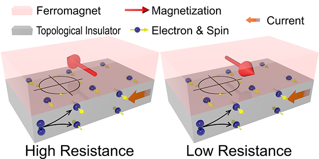
The schematic figure illustrates the concept and behavior of magnetoresistance. The spins are generated in topological insulators. Those at the interface between ferromagnet and topological insulators interact with the ferromagnet and result in either high or low resistance of the device, depending on the relative directions of magnetization and spins. Credit: University of Minnesota

A January 9, 2018 University of Minnesota College of Science and Engineering news release, which originated the news item, expands on the theme,

“Our discovery is one missing piece of the puzzle to improve the future of low-power computing and memory for the semiconductor industry, including brain-like computing and chips for robots and 3D magnetic memory,” said University of Minnesota Robert F. Hartmann Professor of Electrical and Computer Engineering Jian-Ping Wang, director of the Center for Spintronic Materials, Interfaces, and Novel Structures (C-SPIN) based at the University of Minnesota and co-author of the study.

Emerging technology using topological insulators

While magnetic recording still dominates data storage applications, the magnetoresistive random access memory is gradually finding its place in the field of computing memory. From the outside, they are unlike the hard disk drives which have mechanically spinning disks and swinging heads—they are more like any other type of memory. They are chips (solid state) which you’d find being soldered on circuit boards in a computer or mobile device.

Recently, a group of materials called topological insulators has been found to further improve the writing energy efficiency of magnetoresistive random access memory cells in electronics. However, the new device geometry demands a new magnetoresistance phenomenon to accomplish the read function of the memory cell in 3D system and network.

Following the recent discovery of the unidirectional spin Hall magnetoresistance in a conventional metal bilayer material systems, researchers at the University of Minnesota collaborated with colleagues at Pennsylvania State University and demonstrated for the first time the existence of such magnetoresistance in the topological insulator-ferromagnet bilayers.

The study confirms the existence of such unidirectional magnetoresistance and reveals that the adoption of topological insulators, compared to heavy metals, doubles the magnetoresistance performance at 150 Kelvin (-123.15 Celsius). From an application perspective, this work provides the missing piece of the puzzle to create a proposed 3D and cross-bar type computing and memory device involving topological insulators by adding the previously missing or very inconvenient read functionality.

In addition to Wang, researchers involved in this study include Yang Lv, Delin Zhang and Mahdi Jamali from the University of Minnesota Department of Electrical and Computer Engineering and James Kally, Joon Sue Lee and Nitin Samarth from Pennsylvania State University Department of Physics.

This research was funded by the Center for Spintronic Materials, Interfaces and Novel Architectures (C-SPIN) at the University of Minnesota, a Semiconductor Research Corporation program sponsored by the Microelectronics Advanced Research Corp. (MARCO) and the Defense Advanced Research Projects Agency (DARPA).

Here’s a link to and a citation for the paper,

Unidirectional spin-Hall and Rashba−Edelstein magnetoresistance in topological insulator-ferromagnet layer heterostructures by Yang Lv, James Kally, Delin Zhang, Joon Sue Lee, Mahdi Jamali, Nitin Samarth, & Jian-Ping Wang. Nature Communications 9, Article number: 111 (2018) doi:10.1038/s41467-017-02491-3 Published online: 09 January 2018

This is an open access paper.

‘Nano-hashtags’ for Majorana particles?

The ‘nano-hashtags’ are in fact (assuming a minor leap of imagination) nanowires that resemble hashtags.

Scanning electron microscope image of the device wherein clearly a ‘hashtag’ is formed. Credit: Eindhoven University of Technology

An August 23, 2017 news item on ScienceDaily makes the announcement,

In Nature, an international team of researchers from Eindhoven University of Technology [Netherlands], Delft University of Technology [Netherlands] and the University of California — Santa Barbara presents an advanced quantum chip that will be able to provide definitive proof of the mysterious Majorana particles. These particles, first demonstrated in 2012, are their own antiparticle at one and the same time. The chip, which comprises ultrathin networks of nanowires in the shape of ‘hashtags’, has all the qualities to allow Majorana particles to exchange places. This feature is regarded as the smoking gun for proving their existence and is a crucial step towards their use as a building block for future quantum computers.

An August 23, 2017 Eindhoven University press release (also on EurekAlert), which originated the news item, provides some context and information about the work,

In 2012 it was big news: researchers from Delft University of Technology and Eindhoven University of Technology presented the first experimental signatures for the existence of the Majorana fermion. This particle had been predicted in 1937 by the Italian physicist Ettore Majorana and has the distinctive property of also being its own anti-particle. The Majorana particles emerge at the ends of a semiconductor wire, when in contact with a superconductor material.

Smoking gun

While the discovered particles may have properties typical to Majoranas, the most exciting proof could be obtained by allowing two Majorana particles to exchange places, or ‘braid’ as it is scientifically known. “That’s the smoking gun,” suggests Erik Bakkers, one of the researchers from Eindhoven University of Technology. “The behavior we then see could be the most conclusive evidence yet of Majoranas.”

Crossroads

In the Nature paper that is published today [August 23, 2017], Bakkers and his colleagues present a new device that should be able to show this exchanging of Majoranas. In the original experiment in 2012 two Majorana particles were found in a single wire but they were not able to pass each other without immediately destroying the other. Thus the researchers quite literally had to create space. In the presented experiment they formed intersections using the same kinds of nanowire so that four of these intersections form a ‘hashtag’, #, and thus create a closed circuit along which Majoranas are able to move.

Etch and grow

The researchers built their hashtag device starting from scratch. The nanowires are grown from a specially etched substrate such that they form exactly the desired network which they then expose to a stream of aluminium particles, creating layers of aluminium, a superconductor, on specific spots on the wires – the contacts where the Majorana particles emerge. Places that lie ‘in the shadow’ of other wires stay uncovered.

Leap in quality

The entire process happens in a vacuum and at ultra-cold temperature (around -273 degree Celsius). “This ensures very clean, pure contacts,” says Bakkers, “and enables us to make a considerable leap in the quality of this kind of quantum device.” The measurements demonstrate for a number of electronic and magnetic properties that all the ingredients are present for the Majoranas to braid.

Quantum computers

If the researchers succeed in enabling the Majorana particles to braid, they will at once have killed two birds with one stone. Given their robustness, Majoranas are regarded as the ideal building block for future quantum computers that will be able to perform many calculations simultaneously and thus many times faster than current computers. The braiding of two Majorana particles could form the basis for a qubit, the calculation unit of these computers.

Travel around the world

An interesting detail is that the samples have traveled around the world during the fabrication, combining unique and synergetic activities of each research institution. It started in Delft with patterning and etching the substrate, then to Eindhoven for nanowire growth and to Santa Barbara for aluminium contact formation. Finally back to Delft via Eindhoven for the measurements.

Here’s a link to and a citation for the paper,

Epitaxy of advanced nanowire quantum devices by Sasa Gazibegovic, Diana Car, Hao Zhang, Stijn C. Balk, John A. Logan, Michiel W. A. de Moor, Maja C. Cassidy, Rudi Schmits, Di Xu, Guanzhong Wang, Peter Krogstrup, Roy L. M. Op het Veld, Kun Zuo, Yoram Vos, Jie Shen, Daniël Bouman, Borzoyeh Shojaei, Daniel Pennachio, Joon Sue Lee, Petrus J. van Veldhoven, Sebastian Koelling, Marcel A. Verheijen, Leo P. Kouwenhoven, Chris J. Palmstrøm, & Erik P. A. M. Bakkers. Nature 548, 434–438 (24 August 2017) doi:10.1038/nature23468 Published online 23 August 2017

This paper is behind a paywall.

Dexter Johnson has some additional insight (interview with one of the researchers) in an Aug. 29, 2017 posting on his Nanoclast blog (on the IEEE [institute of Electrical and Electronics Engineers] website).