Tag Archives: magnetism

Graphene and its magnetism

I have two news bits about graphene and magnetism. If I understood what I was reading, one is more focused on applications and the other is focused on further establishing the field of valleytronics.

University of Cambridge and superconductivity

A February 8, 2021 news item on Nanowerk announces ‘magnetic work’ from the University of Cambridge (Note: A link has been removed),

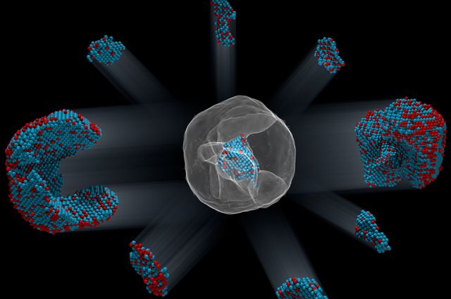
The researchers, led by the University of Cambridge, were able to control the conductivity and magnetism of iron thiophosphate (FePS3), a two-dimensional material which undergoes a transition from an insulator to a metal when compressed. This class of magnetic materials offers new routes to understanding the physics of new magnetic states and superconductivity.

Using new high-pressure techniques, the researchers have shown what happens to magnetic graphene during the transition from insulator to conductor and into its unconventional metallic state, realised only under ultra-high pressure conditions. When the material becomes metallic, it remains magnetic, which is contrary to previous results and provides clues as to how the electrical conduction in the metallic phase works. The newly discovered high-pressure magnetic phase likely forms a precursor to superconductivity so understanding its mechanisms is vital.

Their results, published in the journal Physical Review X, also suggest a way that new materials could be engineered to have combined conduction and magnetic properties, which could be useful in the development of new technologies such as spintronics, which could transform the way in which computers process information.

A February 8, 2021 University of Cambridge press release (also on EurekAlert), which originated the news item, delves into the topic,

Properties of matter can alter dramatically with changing dimensionality. For example, graphene, carbon nanotubes, graphite and diamond are all made of carbon atoms, but have very different properties due to their different structure and dimensionality.

“But imagine if you were also able to change all of these properties by adding magnetism,” said first author Dr Matthew Coak, who is jointly based at Cambridge’s Cavendish Laboratory and the University of Warwick. “A material which could be mechanically flexible and form a new kind of circuit to store information and perform computation. This is why these materials are so interesting, and because they drastically change their properties when put under pressure so we can control their behaviour.”

In a previous study by Sebastian Haines of Cambridge’s Cavendish Laboratory and the Department of Earth Sciences, researchers established that the material becomes a metal at high pressure, and outlined how the crystal structure and arrangement of atoms in the layers of this 2D material change through the transition.

“The missing piece has remained however, the magnetism,” said Coak. “With no experimental techniques able to probe the signatures of magnetism in this material at pressures this high, our international team had to develop and test our own new techniques to make it possible.”

The researchers used new techniques to measure the magnetic structure up to record-breaking high pressures, using specially designed diamond anvils and neutrons to act as the probe of magnetism. They were then able to follow the evolution of the magnetism into the metallic state.

“To our surprise, we found that the magnetism survives and is in some ways strengthened,” co-author Dr Siddharth Saxena, group leader at the Cavendish Laboratory. “This is unexpected, as the newly-freely-roaming electrons in a newly conducting material can no longer be locked to their parent iron atoms, generating magnetic moments there – unless the conduction is coming from an unexpected source.”

In their previous paper, the researchers showed these electrons were ‘frozen’ in a sense. But when they made them flow or move, they started interacting more and more. The magnetism survives, but gets modified into new forms, giving rise to new quantum properties in a new type of magnetic metal.

How a material behaves, whether conductor or insulator, is mostly based on how the electrons, or charge, move around. However, the ‘spin’ of the electrons has been shown to be the source of magnetism. Spin makes electrons behave a bit like tiny bar magnets and point a certain way. Magnetism from the arrangement of electron spins is used in most memory devices: harnessing and controlling it is important for developing new technologies such as spintronics, which could transform the way in which computers process information.

“The combination of the two, the charge and the spin, is key to how this material behaves,” said co-author Dr David Jarvis from the Institut Laue-Langevin, France, who carried out this work as the basis of his PhD studies at the Cavendish Laboratory. “Finding this sort of quantum multi-functionality is another leap forward in the study of these materials.”

“We don’t know exactly what’s happening at the quantum level, but at the same time, we can manipulate it,” said Saxena. “It’s like those famous ‘unknown unknowns’: we’ve opened up a new door to properties of quantum information, but we don’t yet know what those properties might be.”

There are more potential chemical compounds to synthesise than could ever be fully explored and characterised. But by carefully selecting and tuning materials with special properties, it is possible to show the way towards the creation of compounds and systems, but without having to apply huge amounts of pressure.

Additionally, gaining fundamental understanding of phenomena such as low-dimensional magnetism and superconductivity allows researchers to make the next leaps in materials science and engineering, with particular potential in energy efficiency, generation and storage.

As for the case of magnetic graphene, the researchers next plan to continue the search for superconductivity within this unique material. “Now that we have some idea what happens to this material at high pressure, we can make some predictions about what might happen if we try to tune its properties through adding free electrons by compressing it further,” said Coak.

“The thing we’re chasing is superconductivity,” said Saxena. “If we can find a type of superconductivity that’s related to magnetism in a two-dimensional material, it could give us a shot at solving a problem that’s gone back decades.”

The citation and link to the paper are at the end of this blog posting.

Aalto University’s valleytronics

Further north in Finland, researchers at Aalto University make some advances applicable to the field of valleytronics, from a February 5, 2021 Aalto University press release (also on EurekAltert but published February 8, 2021),

Electrons in materials have a property known as ‘spin’, which is responsible for a variety of properties, the most well-known of which is magnetism. Permanent magnets, like the ones used for refrigerator doors, have all the spins in their electrons aligned in the same direction. Scientists refer to this behaviour as ferromagnetism, and the research field of trying to manipulate spin as spintronics.

Down in the quantum world, spins can arrange in more exotic ways, giving rise to frustrated states and entangled magnets. Interestingly, a property similar to spin, known as “the valley,” appears in graphene materials. This unique feature has given rise to the field of valleytronics, which aims to exploit the valley property for emergent physics and information processing, very much like spintronics relies on pure spin physics.

‘Valleytronics would potentially allow encoding information in the quantum valley degree of freedom, similar to how electronics do it with charge and spintronics with the spin.’ Explains Professor Jose Lado, from Aalto’s Department of applied physics, and one of the authors of the work. ‘What’s more, valleytronic devices would offer a dramatic increase in the processing speeds in comparison with electronics, and with much higher stability towards magnetic field noise in comparison with spintronic devices.’

Structures made of rotated, ultra-thin materials provide a rich solid-state platform for designing novel devices. In particular, slightly twisted graphene layers have recently been shown to have exciting unconventional properties, that can ultimately lead to a new family of materials for quantum technologies. These unconventional states which are already being explored depend on electrical charge or spin. The open question is if the valley can also lead to its own family of exciting states.

Making materials for valleytronics

For this goal, it turns out that conventional ferromagnets play a vital role, pushing graphene to the realms of valley physics. In a recent work, Ph.D. student Tobias Wolf, together with Profs. Oded Zilberberg and Gianni Blatter at ETH Zurich, and Prof. Jose Lado at Aalto University, showed a new direction for correlated physics in magnetic van der Waals materials.

The team showed that sandwiching two slightly rotated layers of graphene between a ferromagnetic insulator provides a unique setting for new electronic states. The combination of ferromagnets, graphene’s twist engineering, and relativistic effects force the “valley” property to dominate the electrons behaviour in the material. In particular, the researchers showed how these valley-only states can be tuned electrically, providing a materials platform in which valley-only states can be generated. Building on top of the recent breakthrough in spintronics and van der Waals materials, valley physics in magnetic twisted van der Waals multilayers opens the door to the new realm of correlated twisted valleytronics.

‘Demonstrating these states represents the starting point towards new exotic entangled valley states.’ Said Professor Lado, ‘Ultimately, engineering these valley states can allow realizing quantum entangled valley liquids and fractional quantum valley Hall states. These two exotic states of matter have not been found in nature yet, and would open exciting possibilities towards a potentially new graphene-based platform for topological quantum computing.’

Citations and links

Here’s a link to and a citation for the University of Cambridge research,

Emergent Magnetic Phases in Pressure-Tuned van der Waals Antiferromagnet FePS3 by Matthew J. Coak, David M. Jarvis, Hayrullo Hamidov, Andrew R. Wildes, Joseph A. M. Paddison, Cheng Liu, Charles R. S. Haines, Ngoc T. Dang, Sergey E. Kichanov, Boris N. Savenko, Sungmin Lee, Marie Kratochvílová, Stefan Klotz, Thomas C. Hansen, Denis P. Kozlenko, Je-Geun Park, and Siddharth S. Saxena. Phys. Rev. X 11, 011024 DOI: https://doi.org/10.1103/PhysRevX.11.011024 Published 5 February 2021

This article appears to be open access.

Here’s a link to and a citation for the Aalto University research,

Spontaneous Valley Spirals in Magnetically Encapsulated Twisted Bilayer Graphene by Tobias M. R. Wolf, Oded Zilberberg, Gianni Blatter, and Jose L. Lado. Phys. Rev. Lett. 126, 056803 DOI: https://doi.org/10.1103/PhysRevLett.126.056803 Published 4 February 2021

This paper is behind a paywall.

Graphene flakes bring spintronics a step closer?

Italian researchers are hoping that graphene flakes will be instrumental in the development of spintronics according to a March 14, 2018 news item on phys.org,

Graphene nanoflakes are promising for possible applications in the field of nanoelectronics, and the subject of a study recently published in Nano Letters. These hexagonal nanostructures exhibit quantum effects for modulating current flow. Thanks to their intrinsic magnetic properties, they could also represent a significant step forward in the field of spintronics. The study, conducted via computer analysis and simulations, was led by Massimo Capone.

A March 14, 2018 Scuola Internazionale Superiore di Studi Avanzati (SISSA) press release (also on EurekAlert), which originated the news item, expands on the theme,

“We have been able to observe two key phenomena by analysing the properties of graphene nanoflakes. Both are of great interest for possible future applications” explain Angelo Valli and Massimo Capone, authors of the study together with Adriano Amaricci and Valentina Brosco. The first phenomenon deals with the so-called interference between electrons and is a quantum phenomenon: «In nanoflakes, the electrons interfere with each other in a “destructive” manner if we measure the current in a certain configuration. This means that there is no transmission of current. This is a typically quantum phenomenon, which only occurs at very reduced sizes. By studying the graphene flakes we have understood that it is possible to bring this phenomenon to larger systems, therefore into the nano world and on a scale in which it is observable and can be exploited for possible uses in nanoelectronics». The two researchers explain that in what are called “Quantum interference transistors” destructive interference would be the “OFF” status. For the “ON” status, they say it is sufficient to remove the conditions for interference, thereby enabling the current to flow.

Magnetism and spintronics

But there’s more. In the study, the researchers demonstrated that the nanoflakes present new magnetic properties which are absent, for example, in an entire sheet of graphene: «The magnetism emerges spontaneously at their edges, without any external intervention. This enables the creation of a spin current». The union between the phenomena of quantum interference and of magnetism would allow to obtain almost complete spin polarization, with a huge potential in the field of spintronics, explain the researchers. These properties could be used, for example, in the memorising and processing information technologies, interpreting the spin as binary code. The electron spin, being quantised and having only two possible configurations (which we could call “up” and “down”), is very well suited for this kind of implementation.

Next step: the experimental test

To improve the efficiency of the possible device and the percentage of current polarization the researchers have also developed a protocol that envisages the interaction of the graphene flakes with a surface made of nitrogen and boron. «The results obtained are really interesting. This evidence now awaits the experimental test, to confirm what we have theoretically predicted» concludes Massimo Capone, head of the research and recently awarded the title of Outstanding Referee by the American Physical Society journal; in this way, each year, the journal indicates the male and female scientists who have distinguished themselves for their expertise in collaborating with the journal.

Here’s a link to and a citation for the paper,

Quantum Interference Assisted Spin Filtering in Graphene Nanoflakes by Angelo Valli, Adriano Amaricci, Valentina Brosco, and Massimo Capone. Nano Lett., 2018, 18 (3), pp 2158–2164 DOI: 10.1021/acs.nanolett.8b00453 Publication Date (Web): February 23, 2018

Copyright © 2018 American Chemical Society

This paper is behind a paywall.

Cotton that glows ‘naturally’

Interesting, non? This is causing a bit of excitement but before first, here’s more from the Sept. 14, 2017 American Association for the Advancement of Science (AAAS) news release on EurekAlert,

Cotton that’s grown with molecules that endow appealing properties – like fluorescence or magnetism – may one day eliminate the need for applying chemical treatments to fabrics to achieve such qualities, a new study suggests. Applying synthetic polymers to fabrics can result in a range of appealing properties, but anything added to a fabric can get washed or worn away. Furthermore, while many fibers used in fabrics are synthetic (e.g., polyester), some consumers prefer natural fibers to avoid issues related to sensation, skin irritation, smoothness, and weight. Here, Filipe Natalio and colleagues created cotton fibers that incorporate composites with fluorescent and magnetic properties. They synthesized glucose derivatives that deliver the desirable molecules into the growing ovules of the cotton plant, Gossypium hirsutum. Thus, the molecules are embedded into the cotton fibers themselves, rather than added in the form of a chemical treatment. The resulting fibers exhibited fluorescent or magnetic properties, respectively, although they were weaker than raw fibers lacking the embedded composites, the authors report. They propose that similar techniques could be expanded to other biological systems such as bacteria, bamboo, silk, and flax – essentially opening a new era of “material farming.”

Robert Service’s Sept. 14, 2017 article for Science explores the potential of growing cotton with new properties (Note: A link has been removed),

You may have heard about smartphones and smart homes. But scientists are also designing smart clothes, textiles that can harvest energy, light up, detect pollution, and even communicate with the internet. The problem? Even when they work, these often chemically treated fabrics wear out rapidly over time. Now, researchers have figured out a way to “grow” some of these functions directly into cotton fibers. If the work holds, it could lead to stronger, lighter, and brighter textiles that don’t wear out.

Yet, as the new paper went to press today in Science, editors at the journal were made aware of mistakes in a figure in the supplemental material that prompted them to issue an Editorial Expression of Concern, at least until they receive clarification from the authors. Filipe Natalio, lead author and chemist at the Weizmann Institute of Science in Rehovot, Israel, says the mistakes were errors in the names of pigments used in control experiments, which he is working with the editors to fix.

That hasn’t dampened enthusiasm for the work. “I like this paper a lot,” says Michael Strano, a chemical engineer at the Massachusetts Institute of Technology in Cambridge. The study, he says, lays out a new way to add new functions into plants without changing their genes through genetic engineering. Those approaches face steep regulatory hurdles for widespread use. “Assuming the methods claimed are correct, that’s a big advantage,” Strano says.

Sam Lemonick’s Sept. 14, 2017 article for forbes.com describes how the researchers introduced new properties (in this case, glowing colours) into the cotton plants,

His [Filipe Natalio] team of researchers in Israel, Germany, and Austria used sugar molecules to sneak new properties into cotton. Like a Trojan horse, Natalio says. They tested the method by tagging glucose with a fluorescent dye molecule that glows green when hit with the right kind of light.

They bathed cotton ovules—the part of the plant that makes the fibers—in the glucose. And just like flowers suck up dyed water in grade school experiments, the ovules absorbed the sugar solution and piped the tagged glucose molecules to their cells. As the fibers grew, they took on a yellowish tinge—and glowed bright green under ultraviolet light.

Glowing cotton wasn’t enough for Natalio. It took his group about six months to be sure they were actually delivering the fluorescent protein into the cotton cells and not just coating the fibers in it. Once they were certain, they decided to push the envelope with something very unnatural: magnets.

This time, Natalio’s team modified glucose with the rare earth metal dysprosium, making a molecule that acts like a magnet. And just like they did with the dye, the researchers fed it to cotton ovules and ended up with fibers with magnetic properties.

Both Service and Lemonwick note that the editor of the journal Science (where the research paper was published) Jeremy Berg has written an expression of editorial concern as of Sept. 14, 2017,

In the 15 September [2017] issue, Science published the Report “Biological fabrication of cellulose fibers with tailored properties” by F. Natalio et al. (1). After the issue went to press, we became aware of errors in the labeling and/or identification of the pigments used for the control experiments detailed in figs. S1 and S2 of the supplementary materials. Science is publishing this Editorial Expression of Concern to alert our readers to this information as we await full explanation and clarification from the authors.

The problem seems to be one of terminology (from the Lemonwick article),

… Filipe Natalio, lead author and chemist at the Weizmann Institute of Science in Rehovot, Israel, says the mistakes were errors in the names of pigments used in control experiments, which he is working with the editors to fix.

These things happen. Terminology and spelling aren’t always the same from one country to the next and it can result in confusion. I’m glad to see the discussion is being held openly.

Here’s a link to and a citation for the paper,

Biological fabrication of cellulose fibers with tailored properties by Filipe Natalio, Regina Fuchs, Sidney R. Cohen, Gregory Leitus, Gerhard Fritz-Popovski, Oskar Paris, Michael Kappl, Hans-Jürgen Butt. Science 15 Sep 2017: Vol. 357, Issue 6356, pp. 1118-1122 DOI: 10.1126/science.aan5830

This paper is behind a paywall.

Mapping 23,000 atoms in a nanoparticle

Identification of the precise 3-D coordinates of iron, shown in red, and platinum atoms in an iron-platinum nanoparticle.. Courtesy of Colin Ophus and Florian Nickel/Berkeley Lab

The image of the iron-platinum nanoparticle (referenced in the headline) reminds of foetal ultrasound images. A Feb. 1, 2017 news item on ScienceDaily tells us more,

In the world of the very tiny, perfection is rare: virtually all materials have defects on the atomic level. These imperfections — missing atoms, atoms of one type swapped for another, and misaligned atoms — can uniquely determine a material’s properties and function. Now, UCLA [University of California at Los Angeles] physicists and collaborators have mapped the coordinates of more than 23,000 individual atoms in a tiny iron-platinum nanoparticle to reveal the material’s defects.

The results demonstrate that the positions of tens of thousands of atoms can be precisely identified and then fed into quantum mechanics calculations to correlate imperfections and defects with material properties at the single-atom level.

A Feb. 1, 2017 UCLA news release, which originated the news item, provides more detail about the work,

Jianwei “John” Miao, a UCLA professor of physics and astronomy and a member of UCLA’s California NanoSystems Institute, led the international team in mapping the atomic-level details of the bimetallic nanoparticle, more than a trillion of which could fit within a grain of sand.

“No one has seen this kind of three-dimensional structural complexity with such detail before,” said Miao, who is also a deputy director of the Science and Technology Center on Real-Time Functional Imaging. This new National Science Foundation-funded consortium consists of scientists at UCLA and five other colleges and universities who are using high-resolution imaging to address questions in the physical sciences, life sciences and engineering.

Miao and his team focused on an iron-platinum alloy, a very promising material for next-generation magnetic storage media and permanent magnet applications.

By taking multiple images of the iron-platinum nanoparticle with an advanced electron microscope at Lawrence Berkeley National Laboratory and using powerful reconstruction algorithms developed at UCLA, the researchers determined the precise three-dimensional arrangement of atoms in the nanoparticle.

“For the first time, we can see individual atoms and chemical composition in three dimensions. Everything we look at, it’s new,” Miao said.

The team identified and located more than 6,500 iron and 16,600 platinum atoms and showed how the atoms are arranged in nine grains, each of which contains different ratios of iron and platinum atoms. Miao and his colleagues showed that atoms closer to the interior of the grains are more regularly arranged than those near the surfaces. They also observed that the interfaces between grains, called grain boundaries, are more disordered.

“Understanding the three-dimensional structures of grain boundaries is a major challenge in materials science because they strongly influence the properties of materials,” Miao said. “Now we are able to address this challenge by precisely mapping out the three-dimensional atomic positions at the grain boundaries for the first time.”

The researchers then used the three-dimensional coordinates of the atoms as inputs into quantum mechanics calculations to determine the magnetic properties of the iron-platinum nanoparticle. They observed abrupt changes in magnetic properties at the grain boundaries.

“This work makes significant advances in characterization capabilities and expands our fundamental understanding of structure-property relationships, which is expected to find broad applications in physics, chemistry, materials science, nanoscience and nanotechnology,” Miao said.

In the future, as the researchers continue to determine the three-dimensional atomic coordinates of more materials, they plan to establish an online databank for the physical sciences, analogous to protein databanks for the biological and life sciences. “Researchers can use this databank to study material properties truly on the single-atom level,” Miao said.

Miao and his team also look forward to applying their method called GENFIRE (GENeralized Fourier Iterative Reconstruction) to biological and medical applications. “Our three-dimensional reconstruction algorithm might be useful for imaging like CT scans,” Miao said. Compared with conventional reconstruction methods, GENFIRE requires fewer images to compile an accurate three-dimensional structure.

That means that radiation-sensitive objects can be imaged with lower doses of radiation.

The US Dept. of Energy (DOE) Lawrence Berkeley National Laboratory issued their own Feb. 1, 2017 news release (also on EurekAlert) about the work with a focus on how their equipment made this breakthrough possible (it repeats a little of the info. from the UCLA news release),

Scientists used one of the world’s most powerful electron microscopes to map the precise location and chemical type of 23,000 atoms in an extremely small particle made of iron and platinum.

The 3-D reconstruction reveals the arrangement of atoms in unprecedented detail, enabling the scientists to measure chemical order and disorder in individual grains, which sheds light on the material’s properties at the single-atom level. Insights gained from the particle’s structure could lead to new ways to improve its magnetic performance for use in high-density, next-generation hard drives.

What’s more, the technique used to create the reconstruction, atomic electron tomography (which is like an incredibly high-resolution CT scan), lays the foundation for precisely mapping the atomic composition of other useful nanoparticles. This could reveal how to optimize the particles for more efficient catalysts, stronger materials, and disease-detecting fluorescent tags.

Microscopy data was obtained and analyzed by scientists from the Department of Energy’s Lawrence Berkeley National Laboratory (Berkeley Lab) at the Molecular Foundry, in collaboration with Foundry users from UCLA, Oak Ridge National Laboratory, and the United Kingdom’s University of Birmingham. …

Atoms are the building blocks of matter, and the patterns in which they’re arranged dictate a material’s properties. These patterns can also be exploited to greatly improve a material’s function, which is why scientists are eager to determine the 3-D structure of nanoparticles at the smallest scale possible.

“Our research is a big step in this direction. We can now take a snapshot that shows the positions of all the atoms in a nanoparticle at a specific point in its growth. This will help us learn how nanoparticles grow atom by atom, and it sets the stage for a materials-design approach starting from the smallest building blocks,” says Mary Scott, who conducted the research while she was a Foundry user, and who is now a staff scientist. Scott and fellow Foundry scientists Peter Ercius and Colin Ophus developed the method in close collaboration with Jianwei Miao, a UCLA professor of physics and astronomy.

Their nanoparticle reconstruction builds on an achievement they reported last year in which they measured the coordinates of more than 3,000 atoms in a tungsten needle to a precision of 19 trillionths of a meter (19 picometers), which is many times smaller than a hydrogen atom. Now, they’ve taken the same precision, added the ability to distinguish different elements, and scaled up the reconstruction to include tens of thousands of atoms.

Importantly, their method maps the position of each atom in a single, unique nanoparticle. In contrast, X-ray crystallography and cryo-electron microscopy plot the average position of atoms from many identical samples. These methods make assumptions about the arrangement of atoms, which isn’t a good fit for nanoparticles because no two are alike.

“We need to determine the location and type of each atom to truly understand how a nanoparticle functions at the atomic scale,” says Ercius.

A TEAM approach

The scientists’ latest accomplishment hinged on the use of one of the highest-resolution transmission electron microscopes in the world, called TEAM I. It’s located at the National Center for Electron Microscopy, which is a Molecular Foundry facility. The microscope scans a sample with a focused beam of electrons, and then measures how the electrons interact with the atoms in the sample. It also has a piezo-controlled stage that positions samples with unmatched stability and position-control accuracy.

The researchers began growing an iron-platinum nanoparticle from its constituent elements, and then stopped the particle’s growth before it was fully formed. They placed the “partially baked” particle in the TEAM I stage, obtained a 2-D projection of its atomic structure, rotated it a few degrees, obtained another projection, and so on. Each 2-D projection provides a little more information about the full 3-D structure of the nanoparticle.

They sent the projections to Miao at UCLA, who used a sophisticated computer algorithm to convert the 2-D projections into a 3-D reconstruction of the particle. The individual atomic coordinates and chemical types were then traced from the 3-D density based on the knowledge that iron atoms are lighter than platinum atoms. The resulting atomic structure contains 6,569 iron atoms and 16,627 platinum atoms, with each atom’s coordinates precisely plotted to less than the width of a hydrogen atom.

Translating the data into scientific insights

Interesting features emerged at this extreme scale after Molecular Foundry scientists used code they developed to analyze the atomic structure. For example, the analysis revealed chemical order and disorder in interlocking grains, in which the iron and platinum atoms are arranged in different patterns. This has large implications for how the particle grew and its real-world magnetic properties. The analysis also revealed single-atom defects and the width of disordered boundaries between grains, which was not previously possible in complex 3-D boundaries.

“The important materials science problem we are tackling is how this material transforms from a highly randomized structure, what we call a chemically-disordered structure, into a regular highly-ordered structure with the desired magnetic properties,” says Ophus.

To explore how the various arrangements of atoms affect the nanoparticle’s magnetic properties, scientists from DOE’s Oak Ridge National Laboratory ran computer calculations on the Titan supercomputer at ORNL–using the coordinates and chemical type of each atom–to simulate the nanoparticle’s behavior in a magnetic field. This allowed the scientists to see patterns of atoms that are very magnetic, which is ideal for hard drives. They also saw patterns with poor magnetic properties that could sap a hard drive’s performance.

“This could help scientists learn how to steer the growth of iron-platinum nanoparticles so they develop more highly magnetic patterns of atoms,” says Ercius.

Adds Scott, “More broadly, the imaging technique will shed light on the nucleation and growth of ordered phases within nanoparticles, which isn’t fully theoretically understood but is critically important to several scientific disciplines and technologies.”

The folks at the Berkeley Lab have created a video (notice where the still image from the beginning of this post appears),

The Oak Ridge National Laboratory (ORNL), not wanting to be left out, has been mentioned in a Feb. 3, 2017 news item on ScienceDaily,

… researchers working with magnetic nanoparticles at the University of California, Los Angeles (UCLA), and the US Department of Energy’s (DOE’s) Lawrence Berkeley National Laboratory (Berkeley Lab) approached computational scientists at DOE’s Oak Ridge National Laboratory (ORNL) to help solve a unique problem: to model magnetism at the atomic level using experimental data from a real nanoparticle.

“These types of calculations have been done for ideal particles with ideal crystal structures but not for real particles,” said Markus Eisenbach, a computational scientist at the Oak Ridge Leadership Computing Facility (OLCF), a DOE Office of Science User Facility located at ORNL.

A Feb. 2, 2017 ORNL news release on EurekAlert, which originated the news item, elucidates further on how their team added to the research,

Eisenbach develops quantum mechanical electronic structure simulations that predict magnetic properties in materials. Working with Paul Kent, a computational materials scientist at ORNL’s Center for Nanophase Materials Sciences, the team collaborated with researchers at UCLA and Berkeley Lab’s Molecular Foundry to combine world-class experimental data with world-class computing to do something new–simulate magnetism atom by atom in a real nanoparticle.

Using the new data from the research teams on the West Coast, Eisenbach and Kent were able to precisely model the measured atomic structure, including defects, from a unique iron-platinum (FePt) nanoparticle and simulate its magnetic properties on the 27-petaflop Titan supercomputer at the OLCF.

Electronic structure codes take atomic and chemical structure and solve for the corresponding magnetic properties. However, these structures are typically derived from many 2-D electron microscopy or x-ray crystallography images averaged together, resulting in a representative, but not true, 3-D structure.

“In this case, researchers were able to get the precise 3-D structure for a real particle,” Eisenbach said. “The UCLA group has developed a new experimental technique where they can tell where the atoms are–the coordinates–and the chemical resolution, or what they are — iron or platinum.”

The ORNL news release goes on to describe the work from the perspective of the people who ran the supercompute simulationsr,

A Supercomputing Milestone

Magnetism at the atomic level is driven by quantum mechanics — a fact that has shaken up classical physics calculations and called for increasingly complex, first-principle calculations, or calculations working forward from fundamental physics equations rather than relying on assumptions that reduce computational workload.

For magnetic recording and storage devices, researchers are particularly interested in magnetic anisotropy, or what direction magnetism favors in an atom.

“If the anisotropy is too weak, a bit written to the nanoparticle might flip at room temperature,” Kent said.

To solve for magnetic anisotropy, Eisenbach and Kent used two computational codes to compare and validate results.

To simulate a supercell of about 1,300 atoms from strongly magnetic regions of the 23,000-atom nanoparticle, they used the Linear Scaling Multiple Scattering (LSMS) code, a first-principles density functional theory code developed at ORNL.

“The LSMS code was developed for large magnetic systems and can tackle lots of atoms,” Kent said.

As principal investigator on 2017, 2016, and previous INCITE program awards, Eisenbach has scaled the LSMS code to Titan for a range of magnetic materials projects, and the in-house code has been optimized for Titan’s accelerated architecture, speeding up calculations more than 8 times on the machine’s GPUs. Exceptionally capable of crunching large magnetic systems quickly, the LSMS code received an Association for Computing Machinery Gordon Bell Prize in high-performance computing achievement in 1998 and 2009, and developments continue to enhance the code for new architectures.

Working with Renat Sabirianov at the University of Nebraska at Omaha, the team also ran VASP, a simulation package that is better suited for smaller atom counts, to simulate regions of about 32 atoms.

“With both approaches, we were able to confirm that the local VASP results were consistent with the LSMS results, so we have a high confidence in the simulations,” Eisenbach said.

Computer simulations revealed that grain boundaries have a strong effect on magnetism. “We found that the magnetic anisotropy energy suddenly transitions at the grain boundaries. These magnetic properties are very important,” Miao said.

In the future, researchers hope that advances in computing and simulation will make a full-particle simulation possible — as first-principles calculations are currently too intensive to solve small-scale magnetism for regions larger than a few thousand atoms.

Also, future simulations like these could show how different fabrication processes, such as the temperature at which nanoparticles are formed, influence magnetism and performance.

“There’s a hope going forward that one would be able to use these techniques to look at nanoparticle growth and understand how to optimize growth for performance,” Kent said.

Finally, here’s a link to and a citation for the paper,

Deciphering chemical order/disorder and material properties at the single-atom level by Yongsoo Yang, Chien-Chun Chen, M. C. Scott, Colin Ophus, Rui Xu, Alan Pryor, Li Wu, Fan Sun, Wolfgang Theis, Jihan Zhou, Markus Eisenbach, Paul R. C. Kent, Renat F. Sabirianov, Hao Zeng, Peter Ercius, & Jianwei Miao. Nature 542, 75–79 (02 February 2017) doi:10.1038/nature21042 Published online 01 February 2017

This paper is behind a paywall.

Constructing an autonomous Maxwell’s demon as a self-contained information-powered refrigerator

Aalto University (Finland) was the lead research institution for  INFERNOS, a European Union-funded project concerning Maxwell’s demon. Here’s an excerpt from an Oct. 14, 2013 post featuring the project,

An Oct. 9, 2013 news item on Nanowerk ties together INFERNOS and the ‘demon’,

Maxwell’s Demon is an imaginary creature that the mathematician James Clerk Maxwell created in 1897. The creature could turn heat into work without causing any other change, which violates the second law of thermodynamics. The primary goal of the European project INFERNOS (Information, fluctuations, and energy control in small systems) is to realize experimentally Maxwell’s Demon; in other words, to develop the electronic and biomolecular nanodevices that support this principle.

I like the INFERNOS logo, demon and all,

Logo of the European project INFERNOS (Information, fluctuations, and energy control in small systems).

A Jan. 11, 2016 news item on Nanowerk seems to be highlighting a paper resulting from the INFERNOS project (Note: A link has been removed),

On [a] theoretical level, the thought experiment has been an object of consideration for nearly 150 years, but testing it experimentally has been impossible until the last few years. Making use of nanotechnology, scientists from Aalto University have now succeeded in constructing an autonomous Maxwell’s demon that makes it possible to analyse the microscopic changes in thermodynamics. The research results were recently published in Physical Review Letters (“On-Chip Maxwell’s Demon as an Information-Powered Refrigerator”). The work is part of the forthcoming PhD thesis of MSc Jonne Koski at Aalto University.

An image illustrating the theory underlying the proposed device has been made available,

An autonomous Maxwell's demon. When the demon sees the electron enter the island (1.), it traps the electron with a positive charge (2.). When the electron leaves the island (3.), the demon switches back a negative charge (4.). Image: Jonne Koski.

An autonomous Maxwell’s demon. When the demon sees the electron enter the island (1.), it traps the electron with a positive charge (2.). When the electron leaves the island (3.), the demon switches back a negative charge (4.). Image: Jonne Koski.

A Jan. 11, 2016 Aalto University press release, which originated the news item, provides more technical details,

The system we constructed is a single-electron transistor that is formed by a small metallic island connected to two leads by tunnel junctions made of superconducting materials. The demon connected to the system is also a single-electron transistor that monitors the movement of electrons in the system. When an electron tunnels to the island, the demon traps it with a positive charge. Conversely, when an electron leaves the island, the demon repels it with a negative charge and forces it to move uphill contrary to its potential, which lowers the temperature of the system,’ explains Professor Jukka Pekola.

What makes the demon autonomous or self-contained is that it performs the measurement and feedback operation without outside help. Changes in temperature are indicative of correlation between the demon and the system, or, in simple terms, of how much the demon ‘knows’ about the system. According to Pekola, the research would not have been possible without the Low Temperature Laboratory conditions.

‘We work at extremely low temperatures, so the system is so well isolated that it is possible to register extremely small temperature changes,’ he says.

‘An electronic demon also enables a very large number of repetitions of the measurement and feedback operation in a very short time, whereas those who, elsewhere in the world, used molecules to construct their demons had to contend with not more than a few hundred repetitions.’

The work of the team led by Pekola remains, for the time being, basic research, but in the future, the results obtained may, among other things, pave the way towards reversible computing.

‘As we work with superconducting circuits, it is also possible for us to create qubits of quantum computers. Next, we would like to examine these same phenomena on the quantum level,’ Pekola reveals.

Here’s a link to and a citation for the paper,

On-Chip Maxwell’s Demon as an Information-Powered Refrigerator by J.V. Koski, A. Kutvonen, I.M. Khaymovich, T. Ala-Nissila, and J.P. Pekola. Phys. Rev. Lett. 115, 260602 DOI: http://dx.doi.org/10.1103/PhysRevLett.115.260602 Published 30 December 2015

This paper is behind a paywall.

One final comment, this is the 150th anniversary of Maxwell’s publication of a series of equations explaining the relationships between electric charges and electric and magnetic fields (featured here in a Nov. 27, 2015 posting).

The search for James Clerk Maxwell

The Brits really know how to celebrate an anniversary. In this case it’s the 150th anniversary of James Clerk Maxwell’s electromagnetic theory unifying electricity, magnetism, and light. (My Nov. 27, 2015 posting the first piece here featuring the anniversary and it describes the theory in more detail than you’ll find here.)

As part of the celebration there’s a five-episode series titled: Self Drives: Maxwell’s Equations being broadcast on BBC (British Broadcasting Corporation) 4. Stephen Curry writes about the series in a Dec. 9, 2015 posting on the Guardian science blogs (Note: Links have been removed),

There’s a potent antidote to the “Isn’t this amazing?” school of science communication and it’s called Will Self. In Self Drives: Maxwell’s Equations, which was broadcast recently [you can hear it as a podcast by visiting this site] on BBC Radio 4, the curious curmudgeon takes science to task once again as he goes in search of the mathematical and physical genius behind James Clerk Maxwell.

Over five short episodes, Self’s querulous quest takes him from Maxwell’s birthplace in Edinburgh to his family home in Glenlair, to the radio telescope at Jodrell Bank and the Diamond synchrotron near Oxford, and finally to Cambridge, where Maxwell studied mathematics in his youth and returned in his latter years as one of the nation’s most accomplished scientists to head the university’s Cavendish physics laboratory. Accompanying Self along the way is Akram Khan, the same physics professor who joined the errant writer on his earlier orbit of the Large Hadron Collider at CERN. I would have dubbed Khan Sancho Panza to Self’s Don Quixote but for this particular expedition the characters are reversed. It is Khan who wishes to see the poetry of science, while Self is happier to be grounded in prosaic and flawed reality. At CERN he refused truculently to worship in the cathedral of particle physics, stymied in equal measure by the difficulty of the subject matter and the boosterism of its scientific proponents. Here again the journey is mostly one of disappointment and frustration.

But not for the listener. The quest is far from fruitless, and nor is it lacking in emotional and intellectual force. Self’s documentary is not straight biography – you will find out more about Maxwell’s life and work from Wikipedia – but he has a different target in mind. …

Here’s the pair of explorers,

Will Self, Akram Khan and Maxwell’s infamous equations. Photograph: Laurence Grissell/BBC

Will Self, Akram Khan and Maxwell’s infamous equations. Photograph: Laurence Grissell/BBC

It’s good writing and an intriguing look into communicating science in a way that’s not quite so reverent and/or kid friendly as we tend to be in Canada.

James Clerk Maxwell and his science mashup unified theories of magnetism, electricity, and optics

It’s the 150th anniversary for a series of equations electric charges and electric and magnetic fields that are still being explored. Jon Butterworth in a Nov. 22, 2015 posting on the Guardian science blog network explains (Note: A link has been removed),

The chances are that you are reading this article on some kind of electronic technology. You are definitely seeing it via visible light, unless you have a braille or audio converter. And it probably got to you via wifi or a mobile phone signal. All of those things are understood in terms of the relationships between electric charges and electric and magnetic fields summarised in Maxwell’s [James Clerk Maxwell] equations, published by the Royal Society in 1865, 150 years ago.

Verbally, the equations can be summarised as something like:

Electric and magnetic fields make electric charges move. Electric charges cause electric fields, but there are no magnetic charges. Changes in magnetic fields cause electric fields, and vice versa.

The equations specify precisely how it all happens, but that is the gist of it.

Butterworth got a rare opportunity to see the original manuscript,

 Original manuscript of Maxwell’s seminal paper Photograph: Jon Butterworth/Royal Society [downloaded from http://www.theguardian.com/science/life-and-physics/2015/nov/22/maxwells-equations-150-years-of-light]

Original manuscript of Maxwell’s seminal paper Photograph: Jon Butterworth/Royal Society [downloaded from http://www.theguardian.com/science/life-and-physics/2015/nov/22/maxwells-equations-150-years-of-light]

I love this description from Butterworth,

It was submitted in 1864 but, in a situation familiar to scientists everywhere, was held up in peer review. There’s a letter, dated March 1865, from William Thomson (later Lord Kelvin) saying he was sorry for being slow, that he’d read most of it and it seemed pretty good (“decidely suitable for publication”).

Then, there’s this,

The equations seem to have been very much a bottom-up affair, in that Maxwell collected together a number of known laws which were used to describe various experimental results, and (with a little extra ingredient of his own) fitted them into a unified framework. What is amazing is how much that framework then reveals, both in terms of deep physical principles, and rich physical phenomena.

I’m not excerpting any part of Butterworth’s description of how Maxwell fit these equations together for his unification theory as I think it should be read in its totality.

The section on quantum mechanics is surprising,

Now, one thing Maxwell’s equations don’t contain is quantum mechanics [emphasis mine]. They are classical equations. But if you take the quantum mechnical description of an electron, and you enforce the same charge conservation law/voltage symmetry that was contained in the classical Maxwell’s equations, something marvellous happens [emphasis mine]. The symmetry is denoted “U(1)”, and if you enforce it locally – that it, you say that you have to be allowed make different U(1) type changes to electrons at different points in space, you actually generate the quantum mechanical version of Maxwell’s equations out of nowhere [emphasis mine]. You produce the equations that describe the photon, and the whole of quantum electrodynamics.

I encourage you to read Butterworth’s Nov. 22, 2015 posting where he also mention two related art/science projects and has embedded a video animation of the principles discussed in his posting.

For anyone unfamiliar with Butterworth, there’s this description at the Guardian,

Jon Butterworth is a physics professor at University College London. He is a member of the UCL High Energy Physics group and works on the Atlas experiment at Cern’s Large Hadron Collider. His book Smashing Physics: The Inside Story of the Hunt for the Higgs was published in May 2014

Quantum entanglement and magnetism

A joint Indian/Austrian research team has uncovered the secrets behind why manganese oxides (manganites) have demonstrably different properties when size is reduced. From the Nov. 29, 2011 news item on Nanowerk,

Material properties such as electrical conductivity, magnetic properties or the melting point do not depend on an object’s size and shape. “In India, however, an experiment recently showed that special manganese oxides – so called manganites – exhibit completely different properties, when their size is reduced to tiny grains”, Karsten Held explains.

A team of scientists from the Vienna University of Technology (Austria) and the University of Calcutta (India) investigated this phenomenon – and the new effect could be explained in computer simulations. In a crossover from large crystals to smaller crystals, the distribution of the electrons changes, and so does their energy. This, in turn, changes the electrical and magnetic properties of the crystal. “The phenomenon of quantum entanglement plays a very important role here”, says Professor Karsten Held. “We cannot think of the electrons as classical particles, moving independently of each other, on well-separated paths. The electrons can only be described collectively.” By changing their size, the properties of the manganite-crystals can now be harnessed. Larger crystals are insulators, and they are not magnetic. Tiny crystal pieces on the other hand turn out to be metallic ferromagnets.

Here’s an image of a magnet and crystals,

A magnet and an illustration of manganite cystals (downloaded from the Vienna University of Technology wesite)

Here’s a link to the Nov. 29, 2011 news release from the Vienna University of Technology where you can find additional information in English and German and some pictures.