Tag Archives: Maiken H. Mikkelsen

Point-of-care diagnostics made easier to read with silver nanocubes

Researchers have shown that plasmonics can enhance the fluorescent markers used to signal positive samples in certain types of tests for diseases. A polymer brush coating keeps unwanted biomolecules away while a capture antibody (red) catches biomarkers of disease (clear). A detection antibody (blue) then latches on to the biomarker and emits light from an attached fluorophore (sphere). All of this is sandwiched by a thin layer of gold and a silver nanocube that is attached by a third antibody (green), creating conditions for the fluorophore to emit brighter light. Courtesy: Duke University

A May 12, 2020 news item on Nanowerk announces new work from scientists at Duke University on making point-of-care diagnostics easier to use by making the readouts brighter,

Engineers at Duke University [North Carolina, US] have shown that nanosized silver cubes can make diagnostic tests that rely on fluorescence easier to read by making them more than 150 times brighter. Combined with an emerging point-of-care diagnostic platform already shown capable of detecting small traces of viruses and other biomarkers, the approach could allow such tests to become much cheaper and more widespread.

A May 12, 2020 Duke University news release (also on EurekAlert), which originated the news item, provides more detail about the work,

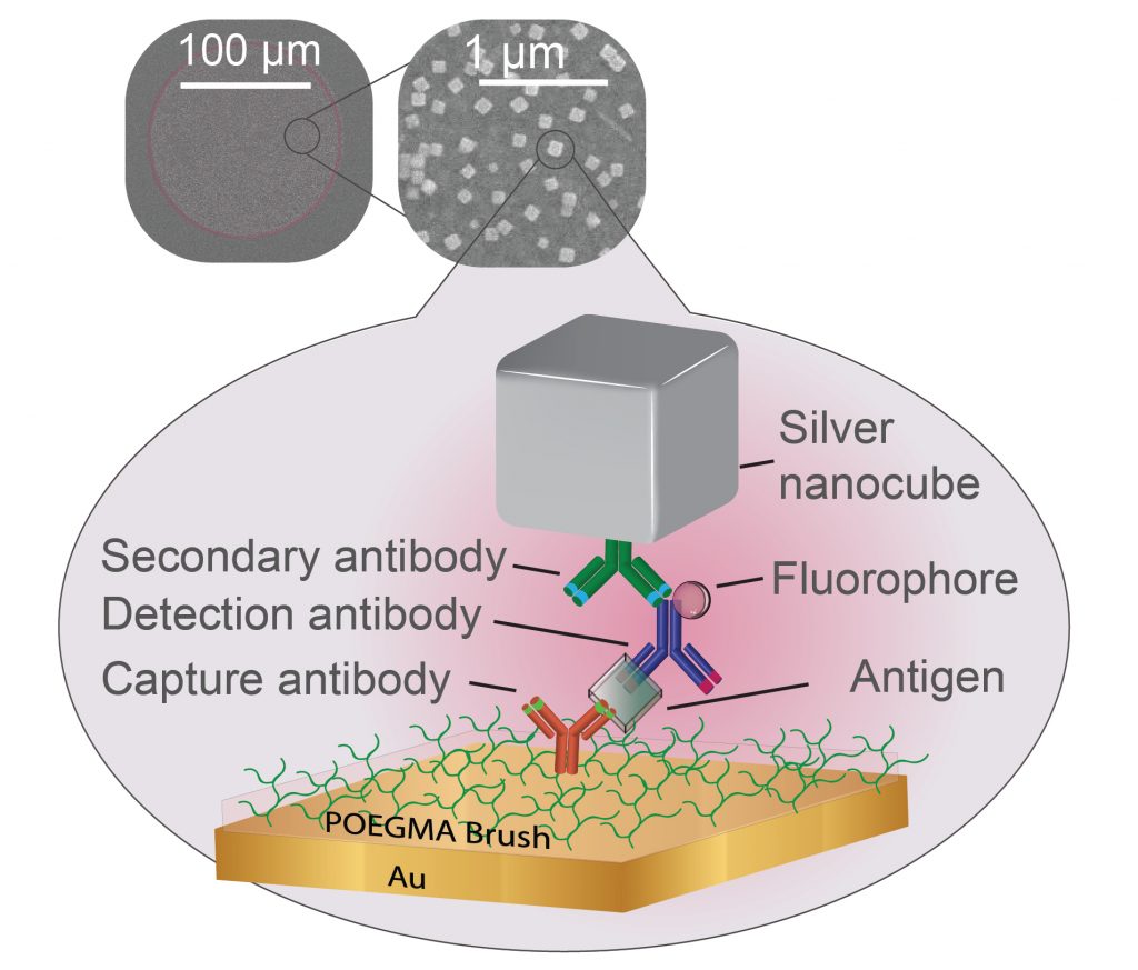
Plasmonics is a scientific field that traps energy in a feedback loop called a plasmon onto the surface of silver nanocubes. When fluorescent molecules are sandwiched between one of these nanocubes and a metal surface, the interaction between their electromagnetic fields causes the molecules to emit light much more vigorously. Maiken Mikkelsen, the James N. and Elizabeth H. Barton Associate Professor of Electrical and Computer Engineering at Duke, has been working with her laboratory at Duke to create new types of hyperspectral cameras and superfast optical signals using plasmonics for nearly a decade.

At the same time, researchers in the laboratory of Ashutosh Chilkoti, the Alan L. Kaganov Distinguished Professor of Biomedical Engineering, have been working on a self-contained, point-of-care diagnostic test that can pick out trace amounts of specific biomarkers from biomedical fluids such as blood. But because the tests rely on fluorescent markers to indicate the presence of the biomarkers, seeing the faint light of a barely positive test requires expensive and bulky equipment.

“Our research has already shown that plasmonics can enhance the brightness of fluorescent molecules tens of thousands of times over,” said Mikkelsen. “Using it to enhance diagnostic assays that are limited by their fluorescence was clearly a very exciting idea.”

“There are not a lot of examples of people using plasmon-enhanced fluorescence for point-of-care diagnostics, and the few that exist have not been yet implemented into clinical practice,” added Daria Semeniak, a graduate student in Chilkoti’s laboratory. “It’s taken us a couple of years, but we think we’ve developed a system that can work.”

In the new paper, researchers from the Chilkoti lab build their super-sensitive diagnostic platform called the D4 Assay onto a thin film of gold, the preferred yin to the plasmonic silver nanocube’s yang. The platform starts with a thin layer of polymer brush coating, which stops anything from sticking to the gold surface that the researchers don’t want to stick there. The researchers then use an ink-jet printer to attach two groups of molecules tailored to latch on to the biomarker that the test is trying to detect. One set is attached permanently to the gold surface and catches one part of the biomarker. The other is washed off of the surface once the test begins, attaches itself to another piece of the biomarker, and flashes light to indicate it’s found its target.

After several minutes pass to allow the reactions to occur, the rest of the sample is washed away, leaving behind only the molecules that have managed to find their biomarker matches, floating like fluorescent beacons tethered to a golden floor.

“The real significance of the assay is the polymer brush coating,” said Chilkoti. “The polymer brush allows us to store all of the tools we need on the chip while maintaining a simple design.”

While the D4 Assay is very good at grabbing small traces of specific biomarkers, if there are only trace amounts, the fluorescent beacons can be difficult to see. The challenge for Mikkelsen and her colleagues was to place their plasmonic silver nanocubes above the beacons in such a way that they supercharged the beacons’ fluorescence.

But as is usually the case, this was easier said than done.

“The distance between the silver nanocubes and the gold film dictates how much brighter the fluorescent molecule becomes,” said Daniela Cruz, a graduate student working in Mikkelsen’s laboratory. “Our challenge was to make the polymer brush coating thick enough to capture the biomarkers–and only the biomarkers of interest–but thin enough to still enhance the diagnostic lights.”

The researchers attempted two approaches to solve this Goldilocks riddle. They first added an electrostatic layer that binds to the detector molecules that carry the fluorescent proteins, creating a sort of “second floor” that the silver nanocubes could sit on top of. They also tried functionalizing the silver nanocubes so that they would stick directly to individual detector molecules on a one-on-one basis.

While both approaches succeeded in boosting the amount of light coming from the beacons, the former showed the best improvement, increasing its fluorescence by more than 150 times. However, this method also requires an extra step of creating a “second floor,” which adds another hurdle to engineering a way to make this work on a commercial point-of-care diagnostic rather than only in a laboratory. And while the fluorescence didn’t improve as much in the second approach, the test’s accuracy did.

“Building microfluidic lab-on-a-chip devices through either approach would take time and resources, but they’re both doable in theory,” said Cassio Fontes, a graduate student in the Chilkoti laboratory. “That’s what the D4 Assay is moving toward.”

And the project is moving forward. Earlier in the year, the researchers used preliminary results from this research to secure a five-year, $3.4 million R01 research award from the National Heart, Lung, and Blood Institute. The collaborators will be working to optimize these fluorescence enhancements while integrating wells, microfluidic channels and other low-cost solutions into a single-step diagnostic device that can run through all of these steps automatically and be read by a common smartphone camera in a low-cost device.

“One of the big challenges in point-of-care tests is the ability to read out results, which usually requires very expensive detectors,” said Mikkelsen. “That’s a major roadblock to having disposable tests to allow patients to monitor chronic diseases at home or for use in low-resource settings. We see this technology not only as a way to get around that bottleneck, but also as a way to enhance the accuracy and threshold of these diagnostic devices.”

Here’s a link to and a citation for the paper,

Ultrabright Fluorescence Readout of an Ink-Jet Printed Immunoassay Using Plasmonic Nanogap Cavities by Daniela F. Cruz, Cassio M. Fontes, Daria Semeniak, Jiani Huang, Angus Hucknall, Ashutosh Chilkoti, Maiken H. Mikkelsen. Nano Lett. 2020, XXXX, XXX, XXX-XXX DOI: https://doi.org/10.1021/acs.nanolett.0c01051 Publication Date:May 6, 2020 Copyright © 2020 American Chemical Society

This paper is behind a paywall.

Bringing multispectral imaging into daily use

Caption: Researchers tested a new technique for printing and imaging in both color and infrared with this image of a parrot. The inlay shows how a simple RGB color scheme was created by building rectangles of varying lengths for each of the colors, as well as individual nanocubes on top of a gold film that create the plasmonic element. Credit: imageBROKER / Alamy Stock Photo

That caption makes a lot more sense after reading the news item and the news release announcing the work. First, there’s the Dec. 15, 2016 news item on ScienceDaily,

Duke University researchers believe they have overcome a longstanding hurdle to producing cheaper, more robust ways to print and image across a range of colors extending into the infrared.

As any mantis shrimp will tell you, there are a wide range of “colors” along the electromagnetic spectrum that humans cannot see but which provide a wealth of information. Sensors that extend into the infrared can, for example, identify thousands of plants and minerals, diagnose cancerous melanomas and predict weather patterns, simply by the spectrum of light they reflect.

Current imaging technologies that can detect infrared wavelengths are expensive and bulky, requiring numerous filters or complex assemblies in front of an infrared photodetector. The need for mechanical movement in such devices reduces their expected lifetime and can be a liability in harsh conditions, such as those experienced by satellites.

A closeup of the colorful parrot picture printed on a thin gold wafer using the new nanocube-based technology. The colors appear off because of the underlying gold, as well as the difficulties that typical cameras have of imaging the new technology. Credit: Maiken Mikkelsen, Duke University

A Dec. 14, 2016 Duke University news release, which originated the news item, provides more detail (Note: A link has been removed),

In a new paper, a team of Duke engineers reveals a manufacturing technique that promises to bring a simplified form of multispectral imaging into daily use. Because the process uses existing materials and fabrication techniques that are inexpensive and easily scalable, it could revolutionize any industry where multispectral imaging or printing is used.

The results appear online December 14 [2016] in the journal Advanced Materials.

“It’s challenging to create sensors that can detect both the visible spectrum and the infrared,” said Maiken Mikkelsen, the Nortel Networks Assistant Professor of Electrical and Computer Engineering and Physics at Duke.

“Traditionally you need different materials that absorb different wavelengths, and that gets very expensive,” Mikkelsen said. “But with our technology, the detectors’ responses are based on structural properties that we design rather than a material’s natural properties. What’s really exciting is that we can pair this with a photodetector scheme to combine imaging in both the visible spectrum and the infrared on a single chip.”

The new technology relies on plasmonics — the use of nanoscale physical phenomena to trap certain frequencies of light.

Engineers fashion silver cubes just 100 nanometers wide and place them only a few nanometers above a thin gold foil. When incoming light strikes the surface of a nanocube, it excites the silver’s electrons, trapping the light’s energy — but only at a certain frequency.

The size of the silver nanocubes and their distance from the base layer of gold determines that frequency, while controlling the spacing between the nanoparticles allows tuning the strength of the absorption. By precisely tailoring these spacings, researchers can make the system respond to any specific color they want, all the way from visible wavelengths out to the infrared.

The challenge facing the engineers is how to build a useful device that could be scalable and inexpensive enough to use in the real world. For that, Mikkelsen turned to her research team, including graduate student Jon Stewart.

“Similar types of materials have been demonstrated before, but they’ve all used expensive techniques that have kept the technology from transitioning to the market,” said Stewart. “We’ve come up with a fabrication scheme that is scalable, doesn’t need a clean room and avoids using million-dollar machines, all while achieving higher frequency sensitivities. It has allowed us to do things in the field that haven’t been done before.”

To build a detector, Mikkelsen and Stewart used a process of light etching and adhesives to pattern the nanocubes into pixels containing different sizes of silver nanocubes, and thus each sensitive to a specific wavelength of light. When incoming light strikes the array, each area responds differently depending on the wavelength of light it is sensitive to. By teasing out how each part of the array responds, a computer can reconstruct what color the original light was.

The technique can be used for printing as well, the team showed. Instead of creating pixels with six sections tuned to respond to specific colors, they created pixels with three bars that reflect three colors: blue, green and red. By controlling the relative lengths of each bar, they can dictate what combination of colors the pixel reflects. It’s a novel take on the classic RGB scheme first used in photography in 1861.

But unlike most other applications, the plasmonic color scheme promises to never fade over time and can be reliably reproduced with tight accuracy time and again. It also allows its adopters to create color schemes in the infrared.

“Again, the exciting part is being able to print in both visible and infrared on the same substrate,” said Mikkelsen. “You could imagine printing an image with a hidden portion in the infrared, or even covering an entire object to tailor its spectral response.”

Here’s a link to and a citation for the paper,

Toward Multispectral Imaging with Colloidal Metasurface Pixels by Jon W. Stewart, Gleb M. Akselrod, David R. Smith, and Maiken H. Mikkelsen. DOI: 10.1002/adma.201602971 Version of Record online: 14 DEC 2016

© 2016 WILEY-VCH Verlag GmbH & Co. KGaA, Weinheim

This paper is behind a paywall. (There is a free preview but it is page 1 only of the paper.)


Liquid nanolaser: the first one

According to an April 24, 2015 news item on Nanowerk, there has been a big discovery at Northwestern University (located in Chicago, Illinois, US),

Northwestern University scientists have developed the first liquid nanoscale laser. And it’s tunable in real time, meaning you can quickly and simply produce different colors, a unique and useful feature. The laser technology could lead to practical applications, such as a new form of a “lab on a chip” for medical diagnostics.

To understand the concept, imagine a laser pointer whose color can be changed simply by changing the liquid inside it, instead of needing a different laser pointer for every desired color.

In addition to changing color in real time, the liquid nanolaser has additional advantages over other nanolasers: it is simple to make, inexpensive to produce and operates at room temperature.

An April 24, 2015 Northwestern University news release by Megan Fellman (also on EurekAlert), which originated the news item, offers a little history buttressed by some technical details (Note: Links have been removed),

Nanoscopic lasers — first demonstrated in 2009 — are only found in research labs today. They are, however, of great interest for advances in technology and for military applications.

“Our study allows us to think about new laser designs and what could be possible if they could actually be made,” said Teri W. Odom, who led the research. “My lab likes to go after new materials, new structures and new ways of putting them together to achieve things not yet imagined. We believe this work represents a conceptual and practical engineering advance for on-demand, reversible control of light from nanoscopic sources.”

The liquid nanolaser in this study is not a laser pointer but a laser device on a chip, Odom explained. The laser’s color can be changed in real time when the liquid dye in the microfluidic channel above the laser’s cavity is changed.

The laser’s cavity is made up of an array of reflective gold nanoparticles, where the light is concentrated around each nanoparticle and then amplified. (In contrast to conventional laser cavities, no mirrors are required for the light to bounce back and forth.) Notably, as the laser color is tuned, the nanoparticle cavity stays fixed and does not change; only the liquid gain around the nanoparticles changes.

The main advantages of very small lasers are:

• They can be used as on-chip light sources for optoelectronic integrated circuits;

• They can be used in optical data storage and lithography;

• They can operate reliably at one wavelength; and

• They should be able to operate much faster than conventional lasers because they are made from metals.

Some technical background

Plasmon lasers are promising nanoscale coherent sources of optical fields because they support ultra-small sizes and show ultra-fast dynamics. Although plasmon lasers have been demonstrated at different spectral ranges, from the ultraviolet to near-infrared, a systematic approach to manipulate the lasing emission wavelength in real time has not been possible.

The main limitation is that only solid gain materials have been used in previous work on plasmon nanolasers; hence, fixed wavelengths were shown because solid materials cannot easily be modified. Odom’s research team has found a way to integrate liquid gain materials with gold nanoparticle arrays to achieve nanoscale plasmon lasing that can be tuned dynamical, reversibly and in real time.

The use of liquid gain materials has two significant benefits:

• The organic dye molecules can be readily dissolved in solvents with different refractive indices. Thus, the dielectric environment around the nanoparticle arrays can be tuned, which also tunes the lasing wavelength.

• The liquid form of gain materials enables the fluid to be manipulated within a microfluidic channel. Thus, dynamic tuning of the lasing emission is possible simply by flowing liquid with different refractive indices. Moreover, as an added benefit of the liquid environment, the lasing-on-chip devices can show long-term stability because the gain molecules can be constantly refreshed.

These nanoscale lasers can be mass-produced with emission wavelengths over the entire gain bandwidth of the dye. Thus, the same fixed nanocavity structure (the same gold nanoparticle array) can exhibit lasing wavelengths that can be tuned over 50 nanometers, from 860 to 910 nanometers, simply by changing the solvent the dye is dissolved in.

Here’s a link to and a citation for the paper,

Real-time tunable lasing from plasmonic nanocavity arrays by Ankun Yang, Thang B. Hoang, Montacer Dridi, Claire Deeb, Maiken H. Mikkelsen, George C. Schatz, & Teri W. Odom. Nature Communications 6, Article number: 6939 doi:10.1038/ncomms7939 Published 20 April 2015

This paper is open access.