Tag Archives: Mark C. Hersam

Brainlike transistor and human intelligence

This brainlike transistor (not a memristor) is important because it functions at room temperature as opposed to others, which require cryogenic temperatures.

A December 20, 2023 Northwestern University news release (received via email; also on EurekAlert) fills in the details,

  • Researchers develop transistor that simultaneously processes and stores information like the human brain
  • Transistor goes beyond categorization tasks to perform associative learning
  • Transistor identified similar patterns, even when given imperfect input
  • Previous similar devices could only operate at cryogenic temperatures; new transistor operates at room temperature, making it more practical

EVANSTON, Ill. — Taking inspiration from the human brain, researchers have developed a new synaptic transistor capable of higher-level thinking.

Designed by researchers at Northwestern University, Boston College and the Massachusetts Institute of Technology (MIT), the device simultaneously processes and stores information just like the human brain. In new experiments, the researchers demonstrated that the transistor goes beyond simple machine-learning tasks to categorize data and is capable of performing associative learning.

Although previous studies have leveraged similar strategies to develop brain-like computing devices, those transistors cannot function outside cryogenic temperatures. The new device, by contrast, is stable at room temperatures. It also operates at fast speeds, consumes very little energy and retains stored information even when power is removed, making it ideal for real-world applications.

The study was published today (Dec. 20 [2023]) in the journal Nature.

“The brain has a fundamentally different architecture than a digital computer,” said Northwestern’s Mark C. Hersam, who co-led the research. “In a digital computer, data move back and forth between a microprocessor and memory, which consumes a lot of energy and creates a bottleneck when attempting to perform multiple tasks at the same time. On the other hand, in the brain, memory and information processing are co-located and fully integrated, resulting in orders of magnitude higher energy efficiency. Our synaptic transistor similarly achieves concurrent memory and information processing functionality to more faithfully mimic the brain.”

Hersam is the Walter P. Murphy Professor of Materials Science and Engineering at Northwestern’s McCormick School of Engineering. He also is chair of the department of materials science and engineering, director of the Materials Research Science and Engineering Center and member of the International Institute for Nanotechnology. Hersam co-led the research with Qiong Ma of Boston College and Pablo Jarillo-Herrero of MIT.

Recent advances in artificial intelligence (AI) have motivated researchers to develop computers that operate more like the human brain. Conventional, digital computing systems have separate processing and storage units, causing data-intensive tasks to devour large amounts of energy. With smart devices continuously collecting vast quantities of data, researchers are scrambling to uncover new ways to process it all without consuming an increasing amount of power. Currently, the memory resistor, or “memristor,” is the most well-developed technology that can perform combined processing and memory function. But memristors still suffer from energy costly switching.

“For several decades, the paradigm in electronics has been to build everything out of transistors and use the same silicon architecture,” Hersam said. “Significant progress has been made by simply packing more and more transistors into integrated circuits. You cannot deny the success of that strategy, but it comes at the cost of high power consumption, especially in the current era of big data where digital computing is on track to overwhelm the grid. We have to rethink computing hardware, especially for AI and machine-learning tasks.”

To rethink this paradigm, Hersam and his team explored new advances in the physics of moiré patterns, a type of geometrical design that arises when two patterns are layered on top of one another. When two-dimensional materials are stacked, new properties emerge that do not exist in one layer alone. And when those layers are twisted to form a moiré pattern, unprecedented tunability of electronic properties becomes possible.

For the new device, the researchers combined two different types of atomically thin materials: bilayer graphene and hexagonal boron nitride. When stacked and purposefully twisted, the materials formed a moiré pattern. By rotating one layer relative to the other, the researchers could achieve different electronic properties in each graphene layer even though they are separated by only atomic-scale dimensions. With the right choice of twist, researchers harnessed moiré physics for neuromorphic functionality at room temperature.

“With twist as a new design parameter, the number of permutations is vast,” Hersam said. “Graphene and hexagonal boron nitride are very similar structurally but just different enough that you get exceptionally strong moiré effects.”

To test the transistor, Hersam and his team trained it to recognize similar — but not identical — patterns. Just earlier this month, Hersam introduced a new nanoelectronic device capable of analyzing and categorizing data in an energy-efficient manner, but his new synaptic transistor takes machine learning and AI one leap further.

“If AI is meant to mimic human thought, one of the lowest-level tasks would be to classify data, which is simply sorting into bins,” Hersam said. “Our goal is to advance AI technology in the direction of higher-level thinking. Real-world conditions are often more complicated than current AI algorithms can handle, so we tested our new devices under more complicated conditions to verify their advanced capabilities.”

First the researchers showed the device one pattern: 000 (three zeros in a row). Then, they asked the AI to identify similar patterns, such as 111 or 101. “If we trained it to detect 000 and then gave it 111 and 101, it knows 111 is more similar to 000 than 101,” Hersam explained. “000 and 111 are not exactly the same, but both are three digits in a row. Recognizing that similarity is a higher-level form of cognition known as associative learning.”

In experiments, the new synaptic transistor successfully recognized similar patterns, displaying its associative memory. Even when the researchers threw curveballs — like giving it incomplete patterns — it still successfully demonstrated associative learning.

“Current AI can be easy to confuse, which can cause major problems in certain contexts,” Hersam said. “Imagine if you are using a self-driving vehicle, and the weather conditions deteriorate. The vehicle might not be able to interpret the more complicated sensor data as well as a human driver could. But even when we gave our transistor imperfect input, it could still identify the correct response.”

The study, “Moiré synaptic transistor with room-temperature neuromorphic functionality,” was primarily supported by the National Science Foundation.

Here’s a link to and a citation for the paper,

Moiré synaptic transistor with room-temperature neuromorphic functionality by Xiaodong Yan, Zhiren Zheng, Vinod K. Sangwan, Justin H. Qian, Xueqiao Wang, Stephanie E. Liu, Kenji Watanabe, Takashi Taniguchi, Su-Yang Xu, Pablo Jarillo-Herrero, Qiong Ma & Mark C. Hersam. Nature volume 624, pages 551–556 (2023) DOI: https://doi.org/10.1038/s41586-023-06791-1 Published online: 20 December 2023 Issue Date: 21 December 2023

This paper is behind a paywall.
100-fold increase in AI energy efficiency

Most people don’t realize how much energy computing, streaming video, and other technologies consume and AI (artificial intelligence) consumes a lot. (For more about work being done in this area, there’s my October 13, 2023 posting about an upcoming ArtSci Salon event in Toronto featuring Laura U. Marks’s recent work ‘Streaming Carbon Footprint’ and my October 16, 2023 posting about how much water is used for AI.)

So this news is welcome, from an October 12, 2023 Northwestern University news release (also received via email and on EurekAlert), Note: Links have been removed,

AI just got 100-fold more energy efficient

Nanoelectronic device performs real-time AI classification without relying on the cloud

– AI is so energy hungry that most data analysis must be performed in the cloud
– New energy-efficient device enables AI tasks to be performed within wearables
– This allows real-time analysis and diagnostics for faster medical interventions
– Researchers tested the device by classifying 10,000 electrocardiogram samples
– The device successfully identified six types of heart beats with 95% accuracy

Northwestern University engineers have developed a new nanoelectronic device that can perform accurate machine-learning classification tasks in the most energy-efficient manner yet. Using 100-fold less energy than current technologies, the device can crunch large amounts of data and perform artificial intelligence (AI) tasks in real time without beaming data to the cloud for analysis.

With its tiny footprint, ultra-low power consumption and lack of lag time to receive analyses, the device is ideal for direct incorporation into wearable electronics (like smart watches and fitness trackers) for real-time data processing and near-instant diagnostics.

To test the concept, engineers used the device to classify large amounts of information from publicly available electrocardiogram (ECG) datasets. Not only could the device efficiently and correctly identify an irregular heartbeat, it also was able to determine the arrhythmia subtype from among six different categories with near 95% accuracy.

The research was published today (Oct. 12 [2023]) in the journal Nature Electronics.

“Today, most sensors collect data and then send it to the cloud, where the analysis occurs on energy-hungry servers before the results are finally sent back to the user,” said Northwestern’s Mark C. Hersam, the study’s senior author. “This approach is incredibly expensive, consumes significant energy and adds a time delay. Our device is so energy efficient that it can be deployed directly in wearable electronics for real-time detection and data processing, enabling more rapid intervention for health emergencies.”

A nanotechnology expert, Hersam is Walter P. Murphy Professor of Materials Science and Engineering at Northwestern’s McCormick School of Engineering. He also is chair of the Department of Materials Science and Engineering, director of the Materials Research Science and Engineering Center and member of the International Institute of Nanotechnology. Hersam co-led the research with Han Wang, a professor at the University of Southern California, and Vinod Sangwan, a research assistant professor at Northwestern.

Before machine-learning tools can analyze new data, these tools must first accurately and reliably sort training data into various categories. For example, if a tool is sorting photos by color, then it needs to recognize which photos are red, yellow or blue in order to accurately classify them. An easy chore for a human, yes, but a complicated — and energy-hungry — job for a machine.

For current silicon-based technologies to categorize data from large sets like ECGs, it takes more than 100 transistors — each requiring its own energy to run. But Northwestern’s nanoelectronic device can perform the same machine-learning classification with just two devices. By reducing the number of devices, the researchers drastically reduced power consumption and developed a much smaller device that can be integrated into a standard wearable gadget.

The secret behind the novel device is its unprecedented tunability, which arises from a mix of materials. While traditional technologies use silicon, the researchers constructed the miniaturized transistors from two-dimensional molybdenum disulfide and one-dimensional carbon nanotubes. So instead of needing many silicon transistors — one for each step of data processing — the reconfigurable transistors are dynamic enough to switch among various steps.

“The integration of two disparate materials into one device allows us to strongly modulate the current flow with applied voltages, enabling dynamic reconfigurability,” Hersam said. “Having a high degree of tunability in a single device allows us to perform sophisticated classification algorithms with a small footprint and low energy consumption.”

To test the device, the researchers looked to publicly available medical datasets. They first trained the device to interpret data from ECGs, a task that typically requires significant time from trained health care workers. Then, they asked the device to classify six types of heart beats: normal, atrial premature beat, premature ventricular contraction, paced beat, left bundle branch block beat and right bundle branch block beat.

The nanoelectronic device was able to identify accurately each arrhythmia type out of 10,000 ECG samples. By bypassing the need to send data to the cloud, the device not only saves critical time for a patient but also protects privacy.

“Every time data are passed around, it increases the likelihood of the data being stolen,” Hersam said. “If personal health data is processed locally — such as on your wrist in your watch — that presents a much lower security risk. In this manner, our device improves privacy and reduces the risk of a breach.”

Hersam imagines that, eventually, these nanoelectronic devices could be incorporated into everyday wearables, personalized to each user’s health profile for real-time applications. They would enable people to make the most of the data they already collect without sapping power.

“Artificial intelligence tools are consuming an increasing fraction of the power grid,” Hersam said. “It is an unsustainable path if we continue relying on conventional computer hardware.”

Here’s a link to and a citation for the paper,

Reconfigurable mixed-kernel heterojunction transistors for personalized support vector machine classification by Xiaodong Yan, Justin H. Qian, Jiahui Ma, Aoyang Zhang, Stephanie E. Liu, Matthew P. Bland, Kevin J. Liu, Xuechun Wang, Vinod K. Sangwan, Han Wang & Mark C. Hersam. Nature Electronics (2023) DOI: https://doi.org/10.1038/s41928-023-01042-7 Published: 12 October 2023

This paper is behind a paywall.

Announcing the ‘memtransistor’

Yet another advance toward ‘brainlike’ computing (how many times have I written this or a variation thereof in the last 10 years? See: Dexter Johnson’s take on the situation at the end of this post): Northwestern University announced their latest memristor research in a February 21, 2018 news item on Nanowerk,

Computer algorithms might be performing brain-like functions, such as facial recognition and language translation, but the computers themselves have yet to operate like brains.

“Computers have separate processing and memory storage units, whereas the brain uses neurons to perform both functions,” said Northwestern University’s Mark C. Hersam. “Neural networks can achieve complicated computation with significantly lower energy consumption compared to a digital computer.”

A February 21, 2018 Northwestern University news release (also on EurekAlert), which originated the news item, provides more information about the latest work from this team,

In recent years, researchers have searched for ways to make computers more neuromorphic, or brain-like, in order to perform increasingly complicated tasks with high efficiency. Now Hersam, a Walter P. Murphy Professor of Materials Science and Engineering in Northwestern’s McCormick School of Engineering, and his team are bringing the world closer to realizing this goal.

The research team has developed a novel device called a “memtransistor,” which operates much like a neuron by performing both memory and information processing. With combined characteristics of a memristor and transistor, the memtransistor also encompasses multiple terminals that operate more similarly to a neural network.

Supported by the National Institute of Standards and Technology and the National Science Foundation, the research was published online today, February 22 [2018], in Nature. Vinod K. Sangwan and Hong-Sub Lee, postdoctoral fellows advised by Hersam, served as the paper’s co-first authors.

The memtransistor builds upon work published in 2015, in which Hersam, Sangwan, and their collaborators used single-layer molybdenum disulfide (MoS2) to create a three-terminal, gate-tunable memristor for fast, reliable digital memory storage. Memristor, which is short for “memory resistors,” are resistors in a current that “remember” the voltage previously applied to them. Typical memristors are two-terminal electronic devices, which can only control one voltage channel. By transforming it into a three-terminal device, Hersam paved the way for memristors to be used in more complex electronic circuits and systems, such as neuromorphic computing.

To develop the memtransistor, Hersam’s team again used atomically thin MoS2 with well-defined grain boundaries, which influence the flow of current. Similar to the way fibers are arranged in wood, atoms are arranged into ordered domains – called “grains” – within a material. When a large voltage is applied, the grain boundaries facilitate atomic motion, causing a change in resistance.

“Because molybdenum disulfide is atomically thin, it is easily influenced by applied electric fields,” Hersam explained. “This property allows us to make a transistor. The memristor characteristics come from the fact that the defects in the material are relatively mobile, especially in the presence of grain boundaries.”

But unlike his previous memristor, which used individual, small flakes of MoS2, Hersam’s memtransistor makes use of a continuous film of polycrystalline MoS2 that comprises a large number of smaller flakes. This enabled the research team to scale up the device from one flake to many devices across an entire wafer.

“When length of the device is larger than the individual grain size, you are guaranteed to have grain boundaries in every device across the wafer,” Hersam said. “Thus, we see reproducible, gate-tunable memristive responses across large arrays of devices.”

After fabricating memtransistors uniformly across an entire wafer, Hersam’s team added additional electrical contacts. Typical transistors and Hersam’s previously developed memristor each have three terminals. In their new paper, however, the team realized a seven-terminal device, in which one terminal controls the current among the other six terminals.

“This is even more similar to neurons in the brain,” Hersam said, “because in the brain, we don’t usually have one neuron connected to only one other neuron. Instead, one neuron is connected to multiple other neurons to form a network. Our device structure allows multiple contacts, which is similar to the multiple synapses in neurons.”

Next, Hersam and his team are working to make the memtransistor faster and smaller. Hersam also plans to continue scaling up the device for manufacturing purposes.

“We believe that the memtransistor can be a foundational circuit element for new forms of neuromorphic computing,” he said. “However, making dozens of devices, as we have done in our paper, is different than making a billion, which is done with conventional transistor technology today. Thus far, we do not see any fundamental barriers that will prevent further scale up of our approach.”

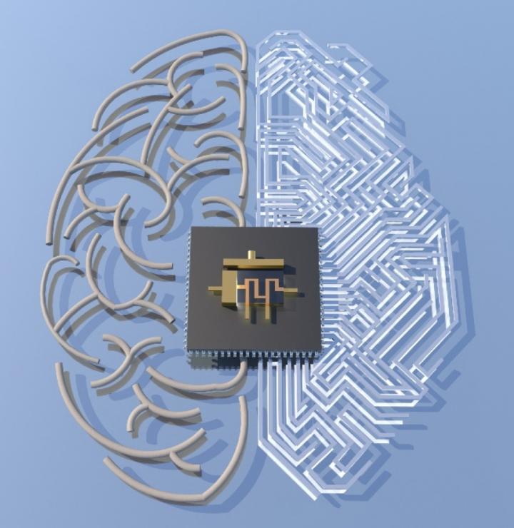
The researchers have made this illustration available,

Caption: This is the memtransistor symbol overlaid on an artistic rendering of a hypothetical circuit layout in the shape of a brain. Credit; Hersam Research Group

Here’s a link to and a citation for the paper,

Multi-terminal memtransistors from polycrystalline monolayer molybdenum disulfide by Vinod K. Sangwan, Hong-Sub Lee, Hadallia Bergeron, Itamar Balla, Megan E. Beck, Kan-Sheng Chen, & Mark C. Hersam. Nature volume 554, pages 500–504 (22 February 2018 doi:10.1038/nature25747 Published online: 21 February 2018

This paper is behind a paywall.

The team’s earlier work referenced in the news release was featured here in an April 10, 2015 posting.

Dexter Johnson

From a Feb. 23, 2018 posting by Dexter Johnson on the Nanoclast blog (on the IEEE [Institute of Electrical and Electronics Engineers] website),

While this all seems promising, one of the big shortcomings in neuromorphic computing has been that it doesn’t mimic the brain in a very important way. In the brain, for every neuron there are a thousand synapses—the electrical signal sent between the neurons of the brain. This poses a problem because a transistor only has a single terminal, hardly an accommodating architecture for multiplying signals.

Now researchers at Northwestern University, led by Mark Hersam, have developed a new device that combines memristors—two-terminal non-volatile memory devices based on resistance switching—with transistors to create what Hersam and his colleagues have dubbed a “memtransistor” that performs both memory storage and information processing.

This most recent research builds on work that Hersam and his team conducted back in 2015 in which the researchers developed a three-terminal, gate-tunable memristor that operated like a kind of synapse.

While this work was recognized as mimicking the low-power computing of the human brain, critics didn’t really believe that it was acting like a neuron since it could only transmit a signal from one artificial neuron to another. This was far short of a human brain that is capable of making tens of thousands of such connections.

“Traditional memristors are two-terminal devices, whereas our memtransistors combine the non-volatility of a two-terminal memristor with the gate-tunability of a three-terminal transistor,” said Hersam to IEEE Spectrum. “Our device design accommodates additional terminals, which mimic the multiple synapses in neurons.”

Hersam believes that these unique attributes of these multi-terminal memtransistors are likely to present a range of new opportunities for non-volatile memory and neuromorphic computing.

If you have the time and the interest, Dexter’s post provides more context,

Ultimate discovery tool?

For anyone familiar with the US nanomedicine scene, Chad Mirkin’s appearance in this announcement from Northwestern University isn’t much of a surprise.  From a June 23, 2016 news item on ScienceDaily,

The discovery power of the gene chip is coming to nanotechnology. A Northwestern University research team is developing a tool to rapidly test millions and perhaps even billions or more different nanoparticles at one time to zero in on the best particle for a specific use.

When materials are miniaturized, their properties—optical, structural, electrical, mechanical and chemical—change, offering new possibilities. But determining what nanoparticle size and composition are best for a given application, such as catalysts, biodiagnostic labels, pharmaceuticals and electronic devices, is a daunting task.

“As scientists, we’ve only just begun to investigate what materials can be made on the nanoscale,” said Northwestern’s Chad A. Mirkin, a world leader in nanotechnology research and its application, who led the study. “Screening a million potentially useful nanoparticles, for example, could take several lifetimes. Once optimized, our tool will enable researchers to pick the winner much faster than conventional methods. We have the ultimate discovery tool.”

A June 23, 2016 Northwestern University news release (also on EurekAlert), which originated the news item, describes the work in more detail,

Using a Northwestern technique that deposits materials on a surface, Mirkin and his team figured out how to make combinatorial libraries of nanoparticles in a very controlled way. (A combinatorial library is a collection of systematically varied structures encoded at specific sites on a surface.) Their study will be published June 24 by the journal Science.

The nanoparticle libraries are much like a gene chip, Mirkin says, where thousands of different spots of DNA are used to identify the presence of a disease or toxin. Thousands of reactions can be done simultaneously, providing results in just a few hours. Similarly, Mirkin and his team’s libraries will enable scientists to rapidly make and screen millions to billions of nanoparticles of different compositions and sizes for desirable physical and chemical properties.

“The ability to make libraries of nanoparticles will open a new field of nanocombinatorics, where size — on a scale that matters — and composition become tunable parameters,” Mirkin said. “This is a powerful approach to discovery science.”

“I liken our combinatorial nanopatterning approach to providing a broad palette of bold colors to an artist who previously had been working with a handful of dull and pale black, white and grey pastels,” said co-author Vinayak P. Dravid, the Abraham Harris Professor of Materials Science and Engineering in the McCormick School of Engineering.

Using five metallic elements — gold, silver, cobalt, copper and nickel — Mirkin and his team developed an array of unique structures by varying every elemental combination. In previous work, the researchers had shown that particle diameter also can be varied deliberately on the 1- to 100-nanometer length scale.

Some of the compositions can be found in nature, but more than half of them have never existed before on Earth. And when pictured using high-powered imaging techniques, the nanoparticles appear like an array of colorful Easter eggs, each compositional element contributing to the palette.

To build the combinatorial libraries, Mirkin and his team used Dip-Pen Nanolithography, a technique developed at Northwestern in 1999, to deposit onto a surface individual polymer “dots,” each loaded with different metal salts of interest. The researchers then heated the polymer dots, reducing the salts to metal atoms and forming a single nanoparticle. The size of the polymer dot can be varied to change the size of the final nanoparticle.

This control of both size and composition of nanoparticles is very important, Mirkin stressed. Having demonstrated control, the researchers used the tool to systematically generate a library of 31 nanostructures using the five different metals.

To help analyze the complex elemental compositions and size/shape of the nanoparticles down to the sub-nanometer scale, the team turned to Dravid, Mirkin’s longtime friend and collaborator. Dravid, founding director of Northwestern’s NUANCE Center, contributed his expertise and the advanced electron microscopes of NUANCE to spatially map the compositional trajectories of the combinatorial nanoparticles.

Now, scientists can begin to study these nanoparticles as well as build other useful combinatorial libraries consisting of billions of structures that subtly differ in size and composition. These structures may become the next materials that power fuel cells, efficiently harvest solar energy and convert it into useful fuels, and catalyze reactions that take low-value feedstocks from the petroleum industry and turn them into high-value products useful in the chemical and pharmaceutical industries.

Here’s a diagram illustrating the work,

 Caption: A combinatorial library of polyelemental nanoparticles was developed using Dip-Pen Nanolithography. This novel nanoparticle library opens up a new field of nanocombinatorics for rapid screening of nanomaterials for a multitude of properties. Credit: Peng-Cheng Chen/James Hedrick

Caption: A combinatorial library of polyelemental nanoparticles was developed using Dip-Pen Nanolithography. This novel nanoparticle library opens up a new field of nanocombinatorics for rapid screening of nanomaterials for a multitude of properties. Credit: Peng-Cheng Chen/James Hedrick

Here’s a link to and a citation for the paper,

Polyelemental nanoparticle libraries by Peng-Cheng Chen, Xiaolong Liu, James L. Hedrick, Zhuang Xie, Shunzhi Wang, Qing-Yuan Lin, Mark C. Hersam, Vinayak P. Dravid, Chad A. Mirkin. Science  24 Jun 2016: Vol. 352, Issue 6293, pp. 1565-1569 DOI: 10.1126/science.aaf8402

This paper is behind a paywall.

A more complex memristor: from two terminals to three for brain-like computing

Researchers have developed a more complex memristor device than has been the case according to an April 6, 2015 Northwestern University news release (also on EurekAlert),

Researchers are always searching for improved technologies, but the most efficient computer possible already exists. It can learn and adapt without needing to be programmed or updated. It has nearly limitless memory, is difficult to crash, and works at extremely fast speeds. It’s not a Mac or a PC; it’s the human brain. And scientists around the world want to mimic its abilities.

Both academic and industrial laboratories are working to develop computers that operate more like the human brain. Instead of operating like a conventional, digital system, these new devices could potentially function more like a network of neurons.

“Computers are very impressive in many ways, but they’re not equal to the mind,” said Mark Hersam, the Bette and Neison Harris Chair in Teaching Excellence in Northwestern University’s McCormick School of Engineering. “Neurons can achieve very complicated computation with very low power consumption compared to a digital computer.”

A team of Northwestern researchers, including Hersam, has accomplished a new step forward in electronics that could bring brain-like computing closer to reality. The team’s work advances memory resistors, or “memristors,” which are resistors in a circuit that “remember” how much current has flowed through them.

“Memristors could be used as a memory element in an integrated circuit or computer,” Hersam said. “Unlike other memories that exist today in modern electronics, memristors are stable and remember their state even if you lose power.”

Current computers use random access memory (RAM), which moves very quickly as a user works but does not retain unsaved data if power is lost. Flash drives, on the other hand, store information when they are not powered but work much slower. Memristors could provide a memory that is the best of both worlds: fast and reliable. But there’s a problem: memristors are two-terminal electronic devices, which can only control one voltage channel. Hersam wanted to transform it into a three-terminal device, allowing it to be used in more complex electronic circuits and systems.

The memristor is of some interest to a number of other parties prominent amongst them, the University of Michigan’s Professor Wei Lu and HP (Hewlett Packard) Labs, both of whom are mentioned in one of my more recent memristor pieces, a June 26, 2014 post.

Getting back to Northwestern,

Hersam and his team met this challenge by using single-layer molybdenum disulfide (MoS2), an atomically thin, two-dimensional nanomaterial semiconductor. Much like the way fibers are arranged in wood, atoms are arranged in a certain direction–called “grains”–within a material. The sheet of MoS2 that Hersam used has a well-defined grain boundary, which is the interface where two different grains come together.

“Because the atoms are not in the same orientation, there are unsatisfied chemical bonds at that interface,” Hersam explained. “These grain boundaries influence the flow of current, so they can serve as a means of tuning resistance.”

When a large electric field is applied, the grain boundary literally moves, causing a change in resistance. By using MoS2 with this grain boundary defect instead of the typical metal-oxide-metal memristor structure, the team presented a novel three-terminal memristive device that is widely tunable with a gate electrode.

“With a memristor that can be tuned with a third electrode, we have the possibility to realize a function you could not previously achieve,” Hersam said. “A three-terminal memristor has been proposed as a means of realizing brain-like computing. We are now actively exploring this possibility in the laboratory.”

Here’s a link to and a citation for the paper,

Gate-tunable memristive phenomena mediated by grain boundaries in single-layer MoS2 by Vinod K. Sangwan, Deep Jariwala, In Soo Kim, Kan-Sheng Chen, Tobin J. Marks, Lincoln J. Lauhon, & Mark C. Hersam. Nature Nanotechnology (2015) doi:10.1038/nnano.2015.56 Published online 06 April 2015

This paper is behind a paywall but there is a few preview available through ReadCube Access.

Dexter Johnson has written about this latest memristor development in an April 9, 2015 posting on his Nanoclast blog (on the IEEE [Institute for Electrical and Electronics Engineers] website) where he notes this (Note: A link has been removed),

The memristor seems to generate fairly polarized debate, especially here on this website in the comments on stories covering the technology. The controversy seems to fall along the lines that the device that HP Labs’ Stan Williams and Greg Snider developed back in 2008 doesn’t exactly line up with the original theory of the memristor proposed by Leon Chua back in 1971.

It seems the ‘debate’ has evolved from issues about how the memristor is categorized. I wonder if there’s still discussion about whether or not HP Labs is attempting to develop a patent thicket of sorts.

A query into the existence of silicene

There’s some fascinating work on silicene at the Argonne National Laboratory which questions current scientific belief as per a July 25, 2014 news item on Nanowerk (Note: A link has been removed),

Sometimes, scientific findings can shake the foundations of what was once held to be true, causing us to step back and re-examine our basic assumptions.

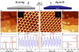
A recent study (“Silicon Growth at the Two-Dimensional Limit on Ag(111)”) at the U.S. Department of Energy’s Argonne National Laboratory has called into question the existence of silicene, thought to be one of the world’s newest and hottest two-dimensional nanomaterials. The study may have great implications to a multi-billion dollar electronics industry that seeks to revolutionize technology at scales 80,000 times smaller than the human hair.

A July 24, 2014 Argonne National Laboratory news release by Justin H.S. Breaux , which originated the news item, describes both silicene and silicon in preparation for the discussion about whether or not silicene exists,

Silicene was proposed as a two-dimensional sheet of silicon atoms that can be created experimentally by super-heating silicon and evaporating atoms onto a silver platform. Silver is the platform of choice because it will not affect the silicon via chemical bonding nor should alloying occur due to its low solubility. During the heating process, as the silicon atoms fall onto the platform, researchers believed that they were arranging themselves in certain ways to create a single sheet of interlocking atoms.

Silicon, on the other hand, exists in three dimensions and is one of the most common elements on Earth. A metal, semiconductor and insulator, purified silicon is extremely stable and has become essential to the integrated circuits and transistors that run most of our computers.

Both silicene and silicon should react immediately with oxygen, but they react slightly differently. In the case of silicon, oxygen breaks some of the silicon bonds of the first one or two atomic layers to form a layer of silicon-oxygen. This, surprisingly, acts a chemical barrier to prevent the decay of the lower layers.

Because it consists of only one layer of silicon atoms, silicene must be handled in a vacuum. Exposure to any amount of oxygen would completely destroy the sample.

This difference is one of the keys to the researchers’ discovery. After depositing the atoms onto the silver platform, initial tests identified that alloy-like surface phases would form until bulk silicon layers, or “platelets” would precipitate out, which has been mistaken as two-dimensional silicene.

The news release next describes how the scientists solved the puzzle,

“Some of the bulk silicon platelets were more than one layer thick,” said Argonne scientist Nathan Guisinger of Argonne’s Center for Nanoscale Materials. “We determined that if we were dealing with multiple layers of silicon atoms, we could bring it out of our ultra-high vacuum chamber and bring it into air and do some other tests.”

“Everybody assumed the sample would immediately decay as soon as they pulled it out of the chamber,” added Northwestern University graduate student Brian Kiraly, one of the principal authors of the study. “We were the first to actually bring it out and perform major experiments outside of the vacuum.”

Each new series of experiments presented a new set of clues that this was, in fact, not silicene.

By examining and categorizing the top layers of the material, the researchers discovered silicon oxide, a sign of oxidation in the top layers. They were also surprised to find that particles from the silver platform alloyed with the silicon at significant depths.

“We found out that what previous researchers identified as silicene is really just a combination of the silicon and the silver,” said Northwestern graduate student Andrew Mannix.

For their final test, the researchers decided to probe the atomic signature of the material.

Materials are made up of systems of atoms that bond and vibrate in unique ways. Raman spectroscopy allows researchers to measure these bonds and vibrations. Housed within the Center for Nanoscale Materials, a DOE Office of Science User Facility, the spectroscope allows researchers to use light to “shift” the position of one atom in a crystal lattice, which in turn causes a shift in the position of its neighbors. Scientists define a material by measuring how strong or weak these bonds are in relation to the frequency at which the atoms vibrate.

The researchers noticed something oddly familiar when looking at the vibrational signatures and frequencies of their sample. Their sample did not exhibit characteristic vibrations of silicene, but it did match those of silicon.

“Having this many research groups and papers potentially be wrong does not happen often,” says Guisinger. “I hope our research helps guide future studies and convincingly demonstrates that silver is not a good platform if you are trying to grow silicene.”

Here’s an image illustrating the vibrational signatures of what scientists had believed to be silicene,

Argonne researchers investigating the properties of silicene (a one-atom thick sheet of silicon atoms) compared scanning tunneling microscope images of atomic silicon growth on silver and atomic silver growth on silicon. The study finds that both growth processes exhibit identical heights and shapes (a, g), indistinguishable honeycomb structures (c, e) and atomic periodicity (d, f). This suggests the growth of bulk silicon on silver, with a silver-induced surface reconstruction, rather than silicene. Courtesy: Argonne National Laboratory

Argonne researchers investigating the properties of silicene (a one-atom thick sheet of silicon atoms) compared scanning tunneling microscope images of atomic silicon growth on silver and atomic silver growth on silicon. The study finds that both growth processes exhibit identical heights and shapes (a, g), indistinguishable honeycomb structures (c, e) and atomic periodicity (d, f). This suggests the growth of bulk silicon on silver, with a silver-induced surface reconstruction, rather than silicene. Courtesy: Argonne National Laboratory

Here’s a link to and a citation for the paper,

Silicon Growth at the Two-Dimensional Limit on Ag(111) by Andrew J. Mannix, Brian Kiraly, Brandon L. Fisher, Mark C. Hersam, and Nathan P. Guisinger. ACS Nano, 2014, 8 (7), pp 7538–7547 DOI: 10.1021/nn503000w Publication Date (Web): July 5, 2014

Copyright © 2014 American Chemical Society

This paper is behind a paywall.

It will be interesting to note what kind of a response the Argonne researchers receive from the scientific community. As for ‘silicene’ items on this blog, there’s a Jan. 14, 2014 posting about work on silicene at the University of Twente (Netherlands). That research was instrumental in helping a student achieve a master’s degree.  While I can describe the Argonne research as fascinating, I imagine the student who got a master’s degree has a different adjective.

Smart ‘curtains’ from the University of California at Berkeley

There’s a weirdly fascinating video that accompanies this research into light-activation and carbon nanotubes,

A Jan. 10, 2014 news item on Nanowerk provides an explanation,

A research team led by Ali Javey, associate professor of electrical engineering and computer sciences [University of California at Berkeley], layered carbon nanotubes – atom-thick rolls of carbon – onto a plastic polycarbonate membrane to create a material that moves quickly in response to light. Within fractions of a second, the nanotubes absorb light, convert it into heat and transfer the heat to the polycarbonate membrane’s surface. The plastic expands in response to the heat, while the nanotube layer does not, causing the two-layered material to bend.

The Jan. 9, 2014 University of California at Berkeley research brief by Sarah Yang, which originated the news item, provides some perspective from lead researcher Javey and a few more details about the research,

“The advantages of this new class of photo-reactive actuator is that it is very easy to make, and it is very sensitive to low-intensity light,” said Javey, who is also a faculty scientist at the Lawrence Berkeley National Lab. “The light from a flashlight is enough to generate a response.”

The researchers described their experiments in a paper published this week in the journal Nature Communications. They were able to tweak the size and chirality – referring to the left or right direction of twist – of the nanotubes to make the material react to different wavelengths of light. The swaths of material they created, dubbed “smart curtains,” could bend or straighten in response to the flick of a light switch.

“We envision these in future smart, energy-efficient buildings,” said Javey. “Curtains made of this material could automatically open or close during the day.”  [emphasis mine]

Other potential applications include light-driven motors and robotics that move toward or away from light, the researchers said.

Here’s a link to and a citation for the paper,

Photoactuators and motors based on carbon nanotubes with selective chirality distributions by Xiaobo Zhang, Zhibin Yu, Chuan Wang, David Zarrouk, Jung-Woo Ted Seo, Jim C. Cheng, Austin D. Buchan, Kuniharu Takei, Yang Zhao, Joel W. Ager, Junjun Zhang, Mark Hettick, Mark C. Hersam, Albert P. Pisano, Ronald S. Fearing, & Ali Javey. Nature Communications 5, Article number: 2983 doi:10.1038/ncomms3983 Published 07 January 2014

The earlier reference to energy-efficient buildings suggests that this work with light-activated curtains is another variation of a ‘smart’ window’ and bears some resemblance to Boris Lamontagne’s (Canada National Research Council) work with curling electrodes which act as blinds in his version of smart glass as per my .Sept. 16, 2011 posting.

Ali Javey has been mentioned here before in a Sept. 15, 2010 post concerning nanotechnology-enabled robot skin.