Tag Archives: metamaterials

Nanosensors use AI to explore the biomolecular world

EPFL scientists have developed AI-powered nanosensors that let researchers track various kinds of biological molecules without disturbing them. Courtesy: École polytechnique fédérale de Lausanne (EPFL)

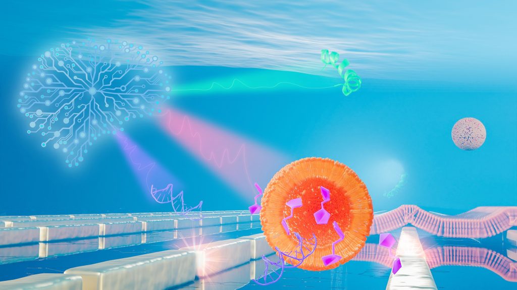
If you look at the big orange dot (representing the nanosensors?), you’ll see those purplish/fuschia objects resemble musical notes (biological molecules?). I think that brainlike object to the left and in light blue is the artificial intelligence (AI) component. (If anyone wants to correct my guesses or identify the bits I can’t, please feel free to add to the Comments for this blog.)

Getting back to my topic, keep the ‘musical notes’ in mind as you read about some of the latest research from l’École polytechnique fédérale de Lausanne (EPFL) in an April 7, 2021 news item on Nanowerk,

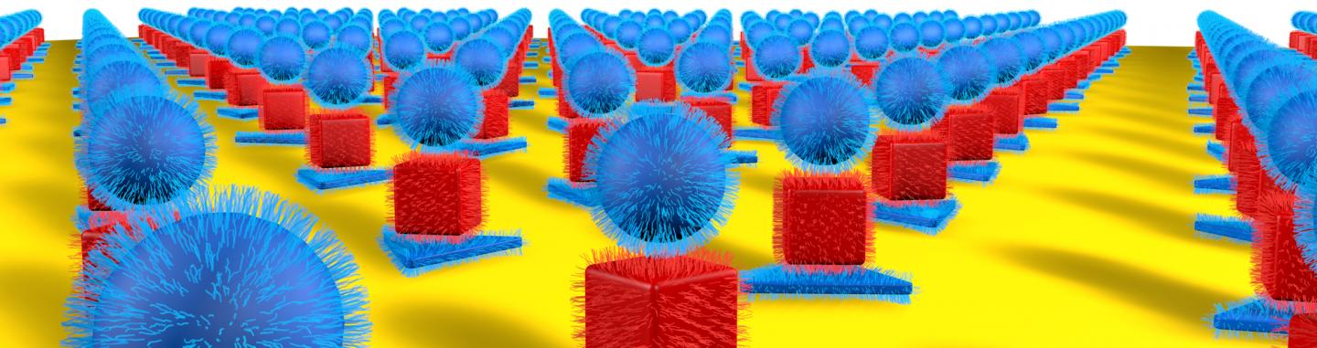
The tiny world of biomolecules is rich in fascinating interactions between a plethora of different agents such as intricate nanomachines (proteins), shape-shifting vessels (lipid complexes), chains of vital information (DNA) and energy fuel (carbohydrates). Yet the ways in which biomolecules meet and interact to define the symphony of life is exceedingly complex.

Scientists at the Bionanophotonic Systems Laboratory in EPFL’s School of Engineering have now developed a new biosensor that can be used to observe all major biomolecule classes of the nanoworld without disturbing them. Their innovative technique uses nanotechnology, metasurfaces, infrared light and artificial intelligence.

To each molecule its own melody

In this nano-sized symphony, perfect orchestration makes physiological wonders such as vision and taste possible, while slight dissonances can amplify into horrendous cacophonies leading to pathologies such as cancer and neurodegeneration.

An April 7, 2021 EPFL press release, which originated the news item, provides more detail,

“Tuning into this tiny world and being able to differentiate between proteins, lipids, nucleic acids and carbohydrates without disturbing their interactions is of fundamental importance for understanding life processes and disease mechanisms,” says Hatice Altug, the head of the Bionanophotonic Systems Laboratory. 

Light, and more specifically infrared light, is at the core of the biosensor developed by Altug’s team. Humans cannot see infrared light, which is beyond the visible light spectrum that ranges from blue to red. However, we can feel it in the form of heat in our bodies, as our molecules vibrate under the infrared light excitation.

Molecules consist of atoms bonded to each other and – depending on the mass of the atoms and the arrangement and stiffness of their bonds – vibrate at specific frequencies. This is similar to the strings on a musical instrument that vibrate at specific frequencies depending on their length. These resonant frequencies are molecule-specific, and they mostly occur in the infrared frequency range of the electromagnetic spectrum. 

“If you imagine audio frequencies instead of infrared frequencies, it’s as if each molecule has its own characteristic melody,” says Aurélian John-Herpin, a doctoral assistant at Altug’s lab and the first author of the publication. “However, tuning into these melodies is very challenging because without amplification, they are mere whispers in a sea of sounds. To make matters worse, their melodies can present very similar motifs making it hard to tell them apart.” 

Metasurfaces and artificial intelligence

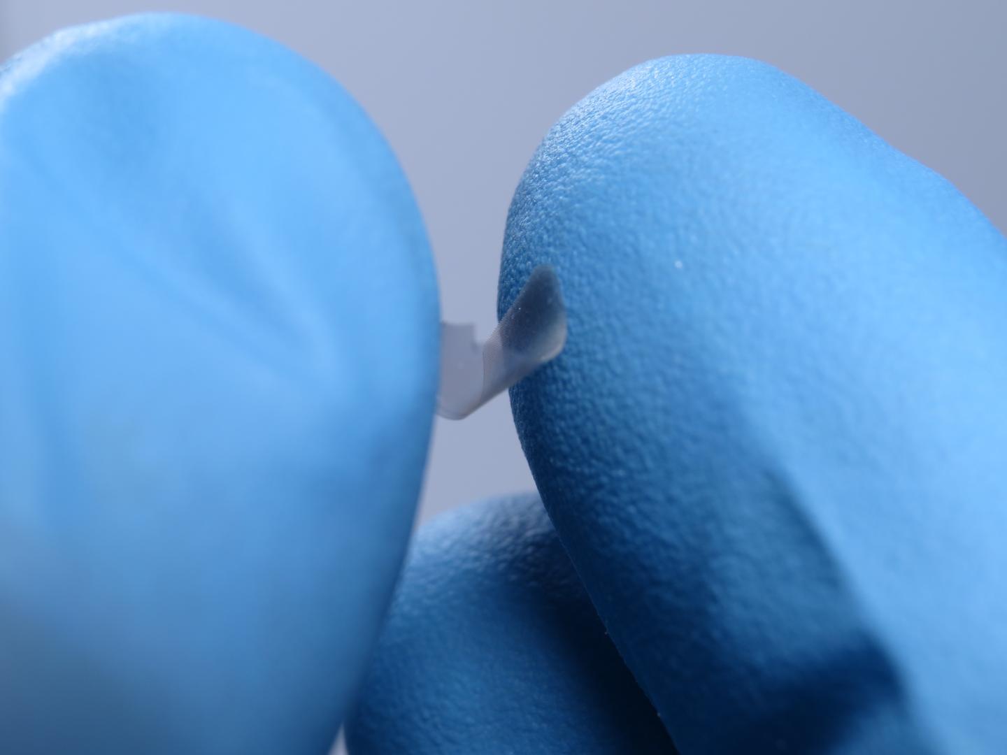
The scientists solved these two issues using metasurfaces and AI. Metasurfaces are man-made materials with outstanding light manipulation capabilities at the nano scale, thereby enabling functions beyond what is otherwise seen in nature. Here, their precisely engineered meta-atoms made out of gold nanorods act like amplifiers of light-matter interactions by tapping into the plasmonic excitations resulting from the collective oscillations of free electrons in metals. “In our analogy, these enhanced interactions make the whispered molecule melodies more audible,” says John-Herpin.

AI is a powerful tool that can be fed with more data than humans can handle in the same amount of time and that can quickly develop the ability to recognize complex patterns from the data. John-Herpin explains, “AI can be imagined as a complete beginner musician who listens to the different amplified melodies and develops a perfect ear after just a few minutes and can tell the melodies apart, even when they are played together – like in an orchestra featuring many instruments simultaneously.” 

The first biosensor of its kind

When the scientists’ infrared metasurfaces are augmented with AI, the new sensor can be used to analyze biological assays featuring multiple analytes simultaneously from the major biomolecule classes and resolving their dynamic interactions. 

“We looked in particular at lipid vesicle-based nanoparticles and monitored their breakage through the insertion of a toxin peptide and the subsequent release of vesicle cargos of nucleotides and carbohydrates, as well as the formation of supported lipid bilayer patches on the metasurface,” says Altug.

This pioneering AI-powered, metasurface-based biosensor will open up exciting perspectives for studying and unraveling inherently complex biological processes, such as intercellular communication via exosomesand the interaction of nucleic acids and carbohydrates with proteins in gene regulation and neurodegeneration. 

“We imagine that our technology will have applications in the fields of biology, bioanalytics and pharmacology – from fundamental research and disease diagnostics to drug development,” says Altug. 

Here’s a link to and a citation for the paper,

Infrared Metasurface Augmented by Deep Learning for Monitoring Dynamics between All Major Classes of Biomolecules by Aurelian John‐Herpin, Deepthy Kavungal. Lea von Mücke, Hatice Altug. Advanced Materials Volume 33, Issue 14 April 8, 2021 2006054 DOI: https://doi.org/10.1002/adma.202006054 First published: 22 February 2021

This paper is open access.

Electron quantum materials, a new field in nanotechnology?

Physicists name and codify new field in nanotechnology: ‘electron quantum metamaterials’

UC Riverside’s Nathaniel Gabor and colleague formulate a vision for the field in a perspective article

Courtesy: University of California at Riverside

Bravo to whomever put the image of a field together together with a subhead that includes the phrases ‘vision for a field’ and ‘perspective article’. It’s even better if you go to the November 5, 2018 University of California at Riverside (UCR) news release (also on EurekAlert) by Iqbal Pittalwala to see the original format,

When two atomically thin two-dimensional layers are stacked on top of each other and one layer is made to rotate against the second layer, they begin to produce patterns — the familiar moiré patterns — that neither layer can generate on its own and that facilitate the passage of light and electrons, allowing for materials that exhibit unusual phenomena. For example, when two graphene layers are overlaid and the angle between them is 1.1 degrees, the material becomes a superconductor.

“It’s a bit like driving past a vineyard and looking out the window at the vineyard rows. Every now and then, you see no rows because you’re looking directly along a row,” said Nathaniel Gabor, an associate professor in the Department of Physics and Astronomy at the University of California, Riverside. “This is akin to what happens when two atomic layers are stacked on top of each other. At certain angles of twist, everything is energetically allowed. It adds up just right to allow for interesting possibilities of energy transfer.”

This is the future of new materials being synthesized by twisting and stacking atomically thin layers, and is still in the “alchemy” stage, Gabor added. To bring it all under one roof, he and physicist Justin C. W. Song of Nanyang Technological University, Singapore, have proposed this field of research be called “electron quantum metamaterials” and have just published a perspective article in Nature Nanotechnology.

“We highlight the potential of engineering synthetic periodic arrays with feature sizes below the wavelength of an electron. Such engineering allows the electrons to be manipulated in unusual ways, resulting in a new range of synthetic quantum metamaterials with unconventional responses,” Gabor said.

Metamaterials are a class of material engineered to produce properties that do not occur naturally. Examples include optical cloaking devices and super-lenses akin to the Fresnel lens that lighthouses use. Nature, too, has adopted such techniques – for example, in the unique coloring of butterfly wings – to manipulate photons as they move through nanoscale structures.

“Unlike photons that scarcely interact with each other, however, electrons in subwavelength structured metamaterials are charged, and they strongly interact,” Gabor said. “The result is an enormous variety of emergent phenomena and radically new classes of interacting quantum metamaterials.”

Gabor and Song were invited by Nature Nanotechnology to write a review paper. But the pair chose to delve deeper and lay out the fundamental physics that may explain much of the research in electron quantum metamaterials. They wrote a perspective paper instead that envisions the current status of the field and discusses its future.

“Researchers, including in our own labs, were exploring a variety of metamaterials but no one had given the field even a name,” said Gabor, who directs the Quantum Materials Optoelectronics lab at UCR. “That was our intent in writing the perspective. We are the first to codify the underlying physics. In a way, we are expressing the periodic table of this new and exciting field. It has been a herculean task to codify all the work that has been done so far and to present a unifying picture. The ideas and experiments have matured, and the literature shows there has been rapid progress in creating quantum materials for electrons. It was time to rein it all in under one umbrella and offer a road map to researchers for categorizing future work.”

In the perspective, Gabor and Song collect early examples in electron metamaterials and distil emerging design strategies for electronic control from them. They write that one of the most promising aspects of the new field occurs when electrons in subwavelength-structure samples interact to exhibit unexpected emergent behavior.

“The behavior of superconductivity in twisted bilayer graphene that emerged was a surprise,” Gabor said. “It shows, remarkably, how electron interactions and subwavelength features could be made to work together in quantum metamaterials to produce radically new phenomena. It is examples like this that paint an exciting future for electronic metamaterials. Thus far, we have only set the stage for a lot of new work to come.”

Gabor, a recipient of a Cottrell Scholar Award and a Canadian Institute for Advanced Research Azrieli Global Scholar Award, was supported by the Air Force Office of Scientific Research Young Investigator Program and a National Science Foundation Division of Materials Research CAREER award.

There is a video illustrating the ideas which is embedded in a November 5, 2018 news item on phys.oirg,


Here’s a link to and a citation for the ‘perspective’ paper,

Electron quantum metamaterials in van der Waals heterostructures by Justin C. W. Song & Nathaniel M. Gabor. Nature Nanotechnology, volume 13, pages986–993 (2018) DOI: https://doi.org/10.1038/s41565-018-0294-9 Published: 05 November 2018

This paper is behind a paywall.

Cloaking devices made from DNA and gold nanoparticles using top-down lithography

This new technique seems promising but there’ve been a lot of ‘cloaking’ devices announced in the years I’ve been blogging and, in all likelihood, I was late to the party so I’m exercising a little caution before getting too excited. For the latest development in cloaking devices, there’s a January 18, 2018 news item on Nanowerk,

Northwestern University researchers have developed a first-of-its-kind technique for creating entirely new classes of optical materials and devices that could lead to light bending and cloaking devices — news to make the ears of Star Trek’s Spock perk up.

Using DNA [deoxyribonucleic acid] as a key tool, the interdisciplinary team took gold nanoparticles of different sizes and shapes and arranged them in two and three dimensions to form optically active superlattices. Structures with specific configurations could be programmed through choice of particle type and both DNA-pattern and sequence to exhibit almost any color across the visible spectrum, the scientists report.

A January 18, 2018 Northwestern University news release (also on EurekAlert) by Megan Fellman, which originated the news item, delves into more detail (Note: Links have been removed),

“Architecture is everything when designing new materials, and we now have a new way to precisely control particle architectures over large areas,” said Chad A. Mirkin, the George B. Rathmann Professor of Chemistry in the Weinberg College of Arts and Sciences at Northwestern. “Chemists and physicists will be able to build an almost infinite number of new structures with all sorts of interesting properties. These structures cannot be made by any known technique.”

The technique combines an old fabrication method — top-down lithography, the same method used to make computer chips — with a new one — programmable self-assembly driven by DNA. The Northwestern team is the first to combine the two to achieve individual particle control in three dimensions.

The study was published online by the journal Science today (Jan. 18). Mirkin and Vinayak P. Dravid and Koray Aydin, both professors in Northwestern’s McCormick School of Engineering, are co-corresponding authors.

Scientists will be able to use the powerful and flexible technique to build metamaterials — materials not found in nature — for a range of applications including sensors for medical and environmental uses.

The researchers used a combination of numerical simulations and optical spectroscopy techniques to identify particular nanoparticle superlattices that absorb specific wavelengths of visible light. The DNA-modified nanoparticles — gold in this case — are positioned on a pre-patterned template made of complementary DNA. Stacks of structures can be made by introducing a second and then a third DNA-modified particle with DNA that is complementary to the subsequent layers.

In addition to being unusual architectures, these materials are stimuli-responsive: the DNA strands that hold them together change in length when exposed to new environments, such as solutions of ethanol that vary in concentration. The change in DNA length, the researchers found, resulted in a change of color from black to red to green, providing extreme tunability of optical properties.

“Tuning the optical properties of metamaterials is a significant challenge, and our study achieves one of the highest tunability ranges achieved to date in optical metamaterials,” said Aydin, assistant professor of electrical engineering and computer science at McCormick.

“Our novel metamaterial platform — enabled by precise and extreme control of gold nanoparticle shape, size and spacing — holds significant promise for next-generation optical metamaterials and metasurfaces,” Aydin said.

The study describes a new way to organize nanoparticles in two and three dimensions. The researchers used lithography methods to drill tiny holes — only one nanoparticle wide — in a polymer resist, creating “landing pads” for nanoparticle components modified with strands of DNA. The landing pads are essential, Mirkin said, since they keep the structures that are grown vertical.

The nanoscopic landing pads are modified with one sequence of DNA, and the gold nanoparticles are modified with complementary DNA. By alternating nanoparticles with complementary DNA, the researchers built nanoparticle stacks with tremendous positional control and over a large area. The particles can be different sizes and shapes (spheres, cubes and disks, for example).

“This approach can be used to build periodic lattices from optically active particles, such as gold, silver and any other material that can be modified with DNA, with extraordinary nanoscale precision,” said Mirkin, director of Northwestern’s International Institute for Nanotechnology.

Mirkin also is a professor of medicine at Northwestern University Feinberg School of Medicine and professor of chemical and biological engineering, biomedical engineering and materials science and engineering in the McCormick School.

The success of the reported DNA programmable assembly required expertise with hybrid (soft-hard) materials and exquisite nanopatterning and lithographic capabilities to achieve the requisite spatial resolution, definition and fidelity across large substrate areas. The project team turned to Dravid, a longtime collaborator of Mirkin’s who specializes in nanopatterning, advanced microscopy and characterization of soft, hard and hybrid nanostructures.

Dravid contributed his expertise and assisted in designing the nanopatterning and lithography strategy and the associated characterization of the new exotic structures. He is the Abraham Harris Professor of Materials Science and Engineering in McCormick and the founding director of the NUANCE center, which houses the advanced patterning, lithography and characterization used in the DNA-programmed structures.

Here’s a link to and a citation for the paper,

Building superlattices from individual nanoparticles via template-confined DNA-mediated assembly by Qing-Yuan Lin, Jarad A. Mason, Zhongyang, Wenjie Zhou, Matthew N. O’Brien, Keith A. Brown, Matthew R. Jones, Serkan Butun, Byeongdu Lee, Vinayak P. Dravid, Koray Aydin, Chad A. Mirkin. Science 18 Jan 2018: eaaq0591 DOI: 10.1126/science.aaq0591

This paper is behind a paywall.

As noted earlier, it could be a while before cloaking devices are made available. In the meantime, you may find this image inspiring,

Caption: Northwestern University researchers have developed a new method to precisely arrange nanoparticles of different sizes and shapes in two and three dimensions, resulting in optically active superlattices. Credit: Northwestern University

Greece and Russia agree to cooperate on quantum and nanotechnology research

I don’t often get a chance to feature Greece here but an April 4, 2016 news item on tornos news (and also on ANAmpa: Athens News Agency [and] Macedonian Press Agency) provides an opportunity,

Greece’s Alternate Minister for Research and Innovation Costas Fotakis and Russian Federation Deputy Minister for Education and Science Ludmila Ogorodova on Friday [April 1, 2016] signed an agreement for cooperation between the two countries in specialist new technologies, such as quantum technology, nanotechnology and related areas.

According to an announcement, the agreement covers four innovative applications in quantum nano-electronics, nanophotonics, quantum information-communication and metamaterials. It extends an invitation to research and technology centres, universities and even public and private research companies to submit proposals in the area of quantum technologies by the end of next June. It envisages financing of up to one million euros in each of the four proposed areas, for programmes to be implemented over 24-36 months.

In spite of the difficult conditions created by the economic crisis, Greece has research centres that have achieved international acclaim and excellence in the emerging field of quantum technology,

So it seems Greece is supplying the quantum expertise and Russia the nanotechnology expertise. It’s a bit surprising that Anatoly Chubais isn’t mentioned since every reference that I’ve ever seen to Russian nanotechnology includes his name as the head of Russia’s state-funded RUSNANO (Russian Nanotechnology Corporation).

Islamic art inspires stretchy metamaterials

A March 16, 2016 article by Jonathan Webb for BBC (British Broadcasting Corporation) News Online describes research on metamaterials from McGill University (Montréal, Canada),

Metamaterials are engineered to have properties that don’t occur naturally, such as getting wider when stretched instead of just longer and thinner.

These perforated rubber sheets made by a Canadian team do just that – and then remain stable in their expanded state until they are squeezed back again.

Such designs could help make expandable stents or spacecraft components.

“In conventional materials, when you pull in one direction it will contract in other directions,” said Dr Ahmad Rafsanjani, from McGill University in Montreal.

“But with ‘auxetic’ materials, due to their internal architecture, when you pull in one direction they expand in the lateral direction.”

A March 16, 2016 article by Shannon Hall in the New Scientist provides more details,

This property comes from their geometric substructure, which when stationary looks like a series of connected squares. When the squares turn relative to each other, however, the material’s density lowers but its thickness increases, allowing it to grow when stretched.

But this twisting means that the materials lose their original shape as they expand. So Ahmad Rafsanjani and Damiano Pasini of McGill University in Montreal, Canada, set out to create a material that would grow when stretched yet keep its form.

To do this, they turned to a beautiful kind of geometry.

“There is a huge library of geometries when you look at Islamic architectures,” says Rafsanjani. The team picked their design from the walls of the Kharraqan towers, two mausoleums built in 1067 and 1093 in the plains in northern Iran.

Both Webb’s and Hall’s articles are embedded with images of the architecture. There’s also a New Scientist video demonstrating stretchability,

The researchers discussed this work in a presentation titled:  Multistable Compliant Auxetic Metamaterials Inspired by Geometric Patterns in Islamic Arts at the American Physical Society’s March 2016 meeting (March 14 – 18, 2016).

A freestanding plate of nanoscale thickness big enough to be ‘hand’led

A rather remarkable achievement is mentioned in a Dec. 3, 2015 news item on Nanotechnology Now,

Researchers at the University of Pennsylvania have now created the thinnest plates that can be picked up and manipulated by hand.

Despite being thousands of times thinner than a sheet of paper and hundreds of times thinner than household cling wrap or aluminum foil, their corrugated plates of aluminum oxide spring back to their original shape after being bent and twisted.

Like cling wrap, comparably thin materials immediately curl up on themselves and get stuck in deformed shapes if they are not stretched on a frame or backed by another material.

Being able to stay in shape without additional support would allow this material, and others designed on its principles, to be used in aviation and other structural applications where low weight is at a premium.

Here’s an image provided by the researchers,

Caption: Even though they are less than 100 nanometers thick, the researchers' plates are strong enough to be picked up by hand and retain their shape after being bent and squeezed. Credit: University of Pennsylvania

Caption: Even though they are less than 100 nanometers thick, the researchers’ plates are strong enough to be picked up by hand and retain their shape after being bent and squeezed. Credit: University of Pennsylvania

A Dec. 3, 2015 University of Pennsylvania news release (also on EurekAlert), which originated the news item, provides more detail,

“Materials on the nanoscale are often much stronger than you’d expect, but they can be hard to use on the macroscale” Bargatin [Igor Bargatin, Assistant Professor] said. “We’ve essentially created a freestanding plate that has nanoscale thickness but is big enough to be handled by hand. That hasn’t been done before.”

Graphene, which can be as thin as a single atom of carbon, has been the poster-child for ultra-thin materials since it’s discovery won the Nobel Prize in Physics in 2010. Graphene is prized for its electrical properties, but its mechanical strength is also very appealing, especially if it could stand on its own. However, graphene and other atomically thin films typically need to be stretched like a canvas in a frame, or even mounted on a backing, to prevent them from curling or clumping up on their own.

“The problem is that frames are heavy, making it impossible to use the intrinsically low weight of these ultra-thin films,” Bargatin said. “Our idea was to use corrugation instead of a frame. That means the structures we make are no longer completely planar, instead, they have a three-dimensional shape that looks like a honeycomb, but they are flat and contiguous and completely freestanding.”

“It’s like an egg carton, but on the nanoscale,” said Purohit. [Prashant Purohit, associate professor]

The researchers’ plates are between 25 and 100 nanometers thick and are made of aluminum oxide, which is deposited one atomic layer at a time to achieve precise control of thickness and their distinctive honeycomb shape.

“Aluminum oxide is actually a ceramic, so something that is ordinarily pretty brittle,” Bargatin said. “You would expect it, from daily experience, to crack very easily. But the plates bend, twist, deform and recover their shape in such a way that you would think they are made out of plastic. The first time we saw it, I could hardly believe it.”

Once finished, the plates’ corrugation provides enhanced stiffness. When held from one end, similarly thin films would readily bend or sag, while the honeycomb plates remain rigid. This guards against the common flaw in un-patterned thin films, where they curl up on themselves.

This ease of deformation is tied to another behavior that makes ultra-thin films hard to use outside controlled conditions: they have the tendency to conform to the shape of any surface and stick to it due to Van der Waals forces. Once stuck, they are hard to remove without damaging them.

Totally flat films are also particularly susceptible to tears or cracks, which can quickly propagate across the entire material.

“If a crack appears in our plates, however, it doesn’t go all the way through the structure,” Davami [Keivan Davami, postdoctoral scholar] said. “It usually stops when it gets to one of the vertical walls of the corrugation.”

The corrugated pattern of the plates is an example of a relatively new field of research: mechanical metamaterials. Like their electromagnetic counterparts, mechanical metamaterials achieve otherwise impossible properties from the careful arrangement of nanoscale features. In mechanical metamaterials’ case, these properties are things like stiffness and strength, rather than their ability to manipulate electromagnetic waves.

Other existing examples of mechanical metamaterials include “nanotrusses,” which are exceptionally lightweight and robust three-dimensional scaffolds made out of nanoscale tubes. The Penn researchers’ plates take the concept of mechanical metamaterials a step further, using corrugation to achieve similar robustness in a plate form and without the holes found in lattice structures.

That combination of traits could be used to make wings for insect-inspired flying robots, or in other applications where the combination of ultra-low thickness and mechanical robustness is critical.

“The wings of insects are a few microns thick, and can’t thinner because they’re made of cells,” Bargatin said. “The thinnest man-made wing material I know of is made by depositing a Mylar film on a frame, and it’s about half a micron thick. Our plates can be ten or more times thinner than that, and don’t need a frame at all. As a result, they weigh as little as than a tenth of a gram per square meter.”

Here’s a link to and a citation for the paper,

Ultralight shape-recovering plate mechanical metamaterials by Keivan Davami, Lin Zhao, Eric Lu, John Cortes, Chen Lin, Drew E. Lilley, Prashant K. Purohit, & Igor Bargatin. Nature Communications 6, Article number: 10019 doi:10.1038/ncomms10019 Published 03 December 2015

This is an open access paper,

Nanoscale light confinement without metal (photonic circuits) at the University of Alberta (Canada)

To be more accurate, this is a step forward towards photonic circuits according to an Aug. 20, 2014 news item on Azonano,

The invention of fibre optics revolutionized the way we share information, allowing us to transmit data at volumes and speeds we’d only previously dreamed of. Now, electrical engineering researchers at the University of Alberta are breaking another barrier, designing nano-optical cables small enough to replace the copper wiring on computer chips.

This could result in radical increases in computing speeds and reduced energy use by electronic devices.

“We’re already transmitting data from continent to continent using fibre optics, but the killer application is using this inside chips for interconnects—that is the Holy Grail,” says Zubin Jacob, an electrical engineering professor leading the research. “What we’ve done is come up with a fundamentally new way of confining light to the nano scale.”

At present, the diameter of fibre optic cables is limited to about one thousandth of a millimetre. Cables designed by graduate student Saman Jahani and Jacob are 10 times smaller—small enough to replace copper wiring still used on computer chips. (To put that into perspective, a dime is about one millimetre thick.)

An Aug. 19, 2014 University of Alberta news release by Richard Cairney (also on EurekAlert), which originated the news item, provides more technical detail and information about funding,

 Jahani and Jacob have used metamaterials to redefine the textbook phenomenon of total internal reflection, discovered 400 years ago by German scientist Johannes Kepler while working on telescopes.

Researchers around the world have been stymied in their efforts to develop effective fibre optics at smaller sizes. One popular solution has been reflective metallic claddings that keep light waves inside the cables. But the biggest hurdle is increased temperatures: metal causes problems after a certain point.

“If you use metal, a lot of light gets converted to heat. That has been the major stumbling block. Light gets converted to heat and the information literally burns up—it’s lost.”

Jacob and Jahani have designed a new, non-metallic metamaterial that enables them to “compress” and contain light waves in the smaller cables without creating heat, slowing the signal or losing data. …

The team’s research is funded by the Natural Sciences and Engineering Research Council of Canada and the Helmholtz-Alberta Initiative.

Jacob and Jahani are now building the metamaterials on a silicon chip to outperform current light confining strategies used in industry.

Given that this work is being performed at the nanoscale and these scientists are located within the Canadian university which houses Canada’s National Institute of Nanotechnology (NINT), the absence of any mention of the NINT comes as a surprise (more about this organization after the link to the researchers’ paper).

Here’s a link to and a citation for the paper,

Transparent subdiffraction optics: nanoscale light confinement without metal by Saman Jahani and Zubin Jacob. Optica, Vol. 1, Issue 2, pp. 96-100 (2014) http://dx.doi.org/10.1364/OPTICA.1.000096

This paper is open access.

In a search for the NINT’s website I found this summary at the University of Alberta’s NINT webpage,

The National Institute for Nanotechnology (NINT) was established in 2001 and is operated as a partnership between the National Research Council and the University of Alberta. Many NINT researchers are affiliated with both the National Research Council and University of Alberta.

NINT is a unique, integrated, multidisciplinary institute involving researchers from fields such as physics, chemistry, engineering, biology, informatics, pharmacy, and medicine. The main focus of the research being done at NINT is the integration of nano-scale devices and materials into complex nanosystems that can be put to practical use. Nanotechnology is a relatively new field of research, so people at NINT are working to discover “design rules” for nanotechnology and to develop platforms for building nanosystems and materials that can be constructed and programmed for a particular application. NINT aims to increase knowledge and support innovation in the area of nanotechnology, as well as to create work that will have long-term relevance and value for Alberta and Canada.

The University of Alberta’s NINT webpage also offers a link to the NINT’s latest rebranded website, The failure to mention the NINT gets more curious when looking at a description of NINT’s programmes one of which is hybrid nanoelectronics (Note: A link has been removed),

Hybrid NanoElectronics provide revolutionary electronic functions that may be utilized by industry through creating circuits that operate using mechanisms unique to the nanoscale. This may include functions that are not possible with conventional circuitry to provide smaller, faster and more energy-efficient components, and extend the development of electronics beyond the end of the roadmap.

After looking at a list of the researchers affiliated with the NINT, it’s apparent that neither Jahani or Jacob are part of that team. Perhaps they have preferred to work independently of the NINT ,which is one of the Canada National Research Council’s institutes.

Atlantic Canada’s Lamda Guard signs deal to test nanocomposite windshield film with Airbus

This story comes from Nova Scotia although you wouldn’t know it if you’d only read the June 5, 2014 news item on Azonano,

Lamda Guard, a company based in Atlantic Canada, has signed an agreement with leading aircraft manufacturer Airbus to test a breakthrough innovation designed to deflect unwanted bright light or laser sources from impacting jetliner flight paths, and causing pilot disorientation or injury.

A June 4, 2014 news release (either from Lamda Guard.com or MTI [metamaterial.com]; Note: More about the multiple webspaces later] and there’s a PDF version here), which originated the news item, provides a little more information about the technology and the perspectives from various stakeholders

Lamda Guard’s innovative thin films utilize metamaterial technology on cockpit windscreens to selectively block and control light coming from any angle even at the highest power levels. “Today marks a milestone in optical applications of nano-composites,” said George Palikaras, President and CEO of Lamda Guard. “Through our collaboration with Airbus we are working to introduce our metamaterial technology, for the first time, as a solution to laser interference in the aviation industry.” The announcement today comes within weeks of the release of an FBI [US Federal Bureau of Investigation] report citing 3,960 aircraft laser strikes in the US in 2013 according to the Federal Aviation Authority (FAA).

Senior Vice President of Innovation Yann Barbaux stated: “At Airbus, we are always on the lookout for new ideas coming from innovative SMEs [small to medium enterprises], such as Lamda Guard. We are very pleased to explore together the potential application of this solution to our aircraft, for the benefit of our customers.”

Over the past year Lamda Guard has been working with the research community at the University of Moncton and the University of New Brunswick, as well as stakeholders, investors and funders to highlight the benefits of nano-composites. The Atlantic Canada Opportunities Agency (ACOA) in particular has played an important role in Lamda Guard’s research and development efforts. In 2012, ACOA assisted Lamda Guard with technology commercialization and recently upgraded its contribution to $500,000 to further assist the company in developing and manufacturing its products for the aviation industry.

The Lamda Guard Airbus partnership marks the first time an optical metamaterial nano-composite has been applied on a large-scale surface.

I tried to find more information about the technology and tracked down this tiny bit, from the What are MetaMaterials? webpage on the MTI website,

A metamaterial typically consists of a multitude of structured unit cells that are comprised of multiple individual elements, which are referred to as meta-atoms. The individual elements are assembled from conventional microscopic materials such as metals and/or plastics, which are arranged in periodic patterns.

MTI’s precisely designed structures are developed with proprietary algorithms, producing a new generation of optical products that are built in state-of-the-art thin film nano-fabrication labs. MTI’s proprietary software accurately predicts the desired design pattern to generate a unique material that meets customer specifications. MTI’s sleek designs mean manufacturers can reduce their cost of materials significantly while increasing performance, e.g. by increasing the light output of an LED bulb or increasing the absorption of light in a solar panel.

Multiple webspaces and presences

While Lamda Guard has a .com presence, you will find yourself on the metamaterial.com website in the Lamda Guard webspace (I suppose you could also call it a subsite) once you start clicking for more information.  In fact, MTI owns three Lamda companies as per this description from the Our Company webpage on the MTI (metamaterial.com) website (Note: Links have been removed),

MTI is an advanced materials and systems engineering company developing and commercializing innovative optical solutions. The company’s core team has over 200 years of combined experience at the forefront of the design and implementation of metamaterials, making MTI a pioneer in bridging the gap between the theoretical and the possible.

MTI specializes in metamaterials, nanotechnology, theoretical and computational electromagnetics. The company’s in-house expertise enables the rapid development of a wide array of metamaterial applications, covering a diverse range of markets.

MTI’s technologies are adaptable and can be custom-designed to suit an industry manufacturer’s specifications allowing for scalability and rapid prototyping with minimum overheads. MTI provides access to world class nano-composite research and development, including specialty, as well as customized, products and licensing of its proprietary solutions to customers ranging from government to private companies.

MTI has three wholly owned subsidiaries:

Lamda Guard Inc. which develops advanced filters to block out selected parts of the light spectrum, protecting the eyes from lasers or other sources of hazardous light.

Lamda Solar Inc. products increase the efficiency of solar panel cells by absorbing more light.

Lamda Lux Inc. technology increases the delivered lumens and reduces the cost of thermal management of LED lighting.

Interestingly, the Lamda Guard Management team‘s (in the Lamda Guard webspace) Chief Science Officer, Dr. Themos Kallos, and Chief Intellectual Property Officer, Dr. Quinton Fivelman, both appear to reside in the UK (assuming I looked at the correct LinkedIn profiles).  Coincidentally, MTI’s contact page lists the company’s headquarters as being in Nova Scotia but Sales, Research and Development would seem to be located in the UK.

Presumably, this company is maximizing its access to government grants and tax incentives in both the UK and Canada. The deal with the Airbus suggests that this has been a successful strategy possibly leading to commercialized technology and, hopefully, jobs.

University of Toronto’s (Canada) invisibility cloak

University of Toronto researchers, Michael Selvanayagam and George V. Eleftheriades, have offered a popular summary of their work. from the popular summary (on the website where they’ve published their academic paper),

We “see” a physical object by detecting electromagnetic waves scattered from the object. A device that can “correct” or cancel that scattering would take the notion of a magic invisibility cloak from the realm of science fiction to reality. In fact, such physical devices already exist, accomplishing their feat based on metamaterials that bend light around the object to be cloaked, “correcting” the scattering. Designing metamaterials with the right light-bending properties for this purpose is, however, quite challenging, and the designs often require a thick “cloak.” An alternative approach to this problem is “active cloaking”: surrounding the object to be cloaked with electromagnetic sources that are carefully tuned to cancel the electromagnetic field scattered by the object. In this work, we demonstrate the first experimental realization of such a thin active cloak for microwaves.

The sources we have used are specially designed antennas and phase shifters, which can be configured into thin layers with flexibility in shape. We have succeeded in cloaking a sizable metallic cylinder by properly tuning the phase of the radiation from the antennas so that the radiation cancels the field scattered by the cylinder. We have gone a step further than cloaking and have also demonstrated how the object can be disguised as another object by tuning the antennas in a controlled way. The catch with active cloaking, however, is that knowledge of the incident field is required to tune the antennas. To tackle this issue, we have discussed some potential solutions that also utilize the antennas as sensors to detect the incident field.

Future work along this line will aim to extend the bandwidth of the cloak (with respect to pulsed incident fields) as well as design active cloaks that can adaptively respond to an incident field.

A Nov. 12, 2013 news item on ScienceDaily, offers information augmenting the popular summary,

Professor George Eleftheriades and PhD student Michael Selvanayagam have designed and tested a new approach to cloaking — by surrounding an object with small antennas that collectively radiate an electromagnetic field. The radiated field cancels out any waves scattering off the cloaked object. Their paper ‘Experimental demonstration of active electromagnetic cloaking’ appears today in the journal Physical Review X.

“We’ve taken an electrical engineering approach, but that’s what we are excited about,” says Eleftheriades. “It’s very practical.”

Picture a mailbox sitting on the street. When light hits the mailbox and bounces back into your eyes, you see the mailbox. When radio waves hit the mailbox and bounce back to your radar detector, you detect the mailbox. Eleftheriades and Selvanyagam’s system wraps the mailbox in a layer of tiny antennas that radiate a field away from the box, cancelling out any waves that would bounce back. In this way, the mailbox becomes undetectable to radar.

The Nov. 13, 2013 University of Toronto news release, which originated the news item and was posted a day later, provides more specific details about the research,

“We’ve demonstrated a different way of doing it,” says Eleftheriades. “It’s very simple: instead of surrounding what you’re trying to cloak with a thick metamaterial shell, we surround it with one layer of tiny antennas, and this layer radiates back a field that cancels the reflections from the object.”

Their experimental demonstration effectively cloaked a metal cylinder from radio waves using one layer of loop antennas. The system can be scaled up to cloak larger objects using more loops, and Eleftheriades says the loops could become printed and flat, like a blanket or skin.

For now, the antenna loops must be manually attuned to the electromagnetic frequency they need to cancel. But in future, researchers say, they could function both as sensors and active antennas, adjusting to different waves in real time, much like the technology behind noise-cancelling headphones.

Work on developing a functional invisibility cloak began around 2006, but early systems were necessarily large and clunky – if you wanted to cloak a car, for example, in practice you would have to completely envelop the vehicle in many layers of metamaterials in order to effectively “shield” it from electromagnetic radiation. The sheer size and inflexibility of that approach makes it impractical for real-world uses.

Earlier attempts to make thin cloaks were not adaptive and active, and could work only for specific small objects.

The cloaking technology holds possiblities that go beyond obvious applications such as hiding military vehicles or conducting surveillance operations. For example, structures that interrupt signals from cellular base stations could be cloaked to allow signals to pass by freely.

The system can also alter the signature of a cloaked object, making it appear bigger, smaller, or even shifting it in space. And though their tests showed the cloaking system works with radio waves, re-tuning it to work with Terahertz (T-rays) or light waves could use the same principle as the necessary antenna technology matures.

For those who feel inclined to explore this work further,

Experimental Demonstration of Active Electromagnetic Cloaking by Michael Selvanayagam and George V. Eleftheriades. Phys. Rev. X (Volume 3 Issue 4) or Phys. Rev. X 3, 041011 (2013) [13 pages]  DOI: 10.1103/PhysRevX.3.041011

Published by the American Physical Society under the terms of the Creative Commons Attribution 3.0 License. Further distribution of this work must maintain attribution to the author(s) and the published article’s title, journal citation, and DOI.

This article is open access.

Protein cages, viruses, and nanoparticles

The Dec. 19, 2012 news release on EurekAlert about a study published by researchers at Aalto University (Finland) describes a project where virus particles are combined with nanoparticles to create new metamaterials,

Scientists from Aalto University, Finland, have succeeded in organising virus particles, protein cages and nanoparticles into crystalline materials. These nanomaterials studied by the Finnish research group are important for applications in sensing, optics, electronics and drug delivery.

… biohybrid superlattices of nanoparticles and proteins would allow the best features of both particle types to be combined. They would comprise the versatility of synthetic nanoparticles and the highly controlled assembly properties of biomolecules.

The gold nanoparticles and viruses adopt a special kind of crystal structure. It does not correspond to any known atomic or molecular crystal structure and it has previously not been observed with nano-sized particles.

Virus particles – the old foes of mankind – can do much more than infect living organisms. Evolution has rendered them with the capability of highly controlled self-assembly properties. Ultimately, by utilising their building blocks we can bring multiple functions to hybrid materials that consist of both living and synthetic matter, Kostiainen [Mauri A. Kostiainen, postdoctoral researcher] trusts.

The article which has been published in Nature Nanotechnology is free,

Electrostatic assembly of binary nanoparticle superlattices using protein cages by Mauri A. Kostiainen, Panu Hiekkataipale, Ari Laiho, Vincent Lemieux, Jani Seitsonen, Janne Ruokolainen & Pierpaolo Ceci in Nature Nanotechnology (2012) doi:10.1038/nnano.2012.220  Published online 16 December 2012

There’s a video demonstrating the assembly,

From the YouTube page, here’s a description of what the video is demonstrating,

Aalto University-led research group shows that CCMV virus or ferritin protein cages can be used to guide the assembly of RNA molecules or iron oxide nanoparticles into three-dimensional binary superlattices. The lattices are formed through tuneable electrostatic interactions with charged gold nanoparticles.

Bravo and thank  you to  Kostiainen who seems to have written the news release and prepared all of the additional materials (image and video). There are university press offices that could take lessons from Kostiainen’s efforts to communicate about the work.