Tag Archives: Molecular Foundry

Mapping 23,000 atoms in a nanoparticle

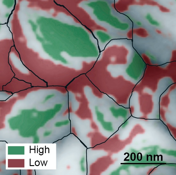
Identification of the precise 3-D coordinates of iron, shown in red, and platinum atoms in an iron-platinum nanoparticle.. Courtesy of Colin Ophus and Florian Nickel/Berkeley Lab

The image of the iron-platinum nanoparticle (referenced in the headline) reminds of foetal ultrasound images. A Feb. 1, 2017 news item on ScienceDaily tells us more,

In the world of the very tiny, perfection is rare: virtually all materials have defects on the atomic level. These imperfections — missing atoms, atoms of one type swapped for another, and misaligned atoms — can uniquely determine a material’s properties and function. Now, UCLA [University of California at Los Angeles] physicists and collaborators have mapped the coordinates of more than 23,000 individual atoms in a tiny iron-platinum nanoparticle to reveal the material’s defects.

The results demonstrate that the positions of tens of thousands of atoms can be precisely identified and then fed into quantum mechanics calculations to correlate imperfections and defects with material properties at the single-atom level.

A Feb. 1, 2017 UCLA news release, which originated the news item, provides more detail about the work,

Jianwei “John” Miao, a UCLA professor of physics and astronomy and a member of UCLA’s California NanoSystems Institute, led the international team in mapping the atomic-level details of the bimetallic nanoparticle, more than a trillion of which could fit within a grain of sand.

“No one has seen this kind of three-dimensional structural complexity with such detail before,” said Miao, who is also a deputy director of the Science and Technology Center on Real-Time Functional Imaging. This new National Science Foundation-funded consortium consists of scientists at UCLA and five other colleges and universities who are using high-resolution imaging to address questions in the physical sciences, life sciences and engineering.

Miao and his team focused on an iron-platinum alloy, a very promising material for next-generation magnetic storage media and permanent magnet applications.

By taking multiple images of the iron-platinum nanoparticle with an advanced electron microscope at Lawrence Berkeley National Laboratory and using powerful reconstruction algorithms developed at UCLA, the researchers determined the precise three-dimensional arrangement of atoms in the nanoparticle.

“For the first time, we can see individual atoms and chemical composition in three dimensions. Everything we look at, it’s new,” Miao said.

The team identified and located more than 6,500 iron and 16,600 platinum atoms and showed how the atoms are arranged in nine grains, each of which contains different ratios of iron and platinum atoms. Miao and his colleagues showed that atoms closer to the interior of the grains are more regularly arranged than those near the surfaces. They also observed that the interfaces between grains, called grain boundaries, are more disordered.

“Understanding the three-dimensional structures of grain boundaries is a major challenge in materials science because they strongly influence the properties of materials,” Miao said. “Now we are able to address this challenge by precisely mapping out the three-dimensional atomic positions at the grain boundaries for the first time.”

The researchers then used the three-dimensional coordinates of the atoms as inputs into quantum mechanics calculations to determine the magnetic properties of the iron-platinum nanoparticle. They observed abrupt changes in magnetic properties at the grain boundaries.

“This work makes significant advances in characterization capabilities and expands our fundamental understanding of structure-property relationships, which is expected to find broad applications in physics, chemistry, materials science, nanoscience and nanotechnology,” Miao said.

In the future, as the researchers continue to determine the three-dimensional atomic coordinates of more materials, they plan to establish an online databank for the physical sciences, analogous to protein databanks for the biological and life sciences. “Researchers can use this databank to study material properties truly on the single-atom level,” Miao said.

Miao and his team also look forward to applying their method called GENFIRE (GENeralized Fourier Iterative Reconstruction) to biological and medical applications. “Our three-dimensional reconstruction algorithm might be useful for imaging like CT scans,” Miao said. Compared with conventional reconstruction methods, GENFIRE requires fewer images to compile an accurate three-dimensional structure.

That means that radiation-sensitive objects can be imaged with lower doses of radiation.

The US Dept. of Energy (DOE) Lawrence Berkeley National Laboratory issued their own Feb. 1, 2017 news release (also on EurekAlert) about the work with a focus on how their equipment made this breakthrough possible (it repeats a little of the info. from the UCLA news release),

Scientists used one of the world’s most powerful electron microscopes to map the precise location and chemical type of 23,000 atoms in an extremely small particle made of iron and platinum.

The 3-D reconstruction reveals the arrangement of atoms in unprecedented detail, enabling the scientists to measure chemical order and disorder in individual grains, which sheds light on the material’s properties at the single-atom level. Insights gained from the particle’s structure could lead to new ways to improve its magnetic performance for use in high-density, next-generation hard drives.

What’s more, the technique used to create the reconstruction, atomic electron tomography (which is like an incredibly high-resolution CT scan), lays the foundation for precisely mapping the atomic composition of other useful nanoparticles. This could reveal how to optimize the particles for more efficient catalysts, stronger materials, and disease-detecting fluorescent tags.

Microscopy data was obtained and analyzed by scientists from the Department of Energy’s Lawrence Berkeley National Laboratory (Berkeley Lab) at the Molecular Foundry, in collaboration with Foundry users from UCLA, Oak Ridge National Laboratory, and the United Kingdom’s University of Birmingham. …

Atoms are the building blocks of matter, and the patterns in which they’re arranged dictate a material’s properties. These patterns can also be exploited to greatly improve a material’s function, which is why scientists are eager to determine the 3-D structure of nanoparticles at the smallest scale possible.

“Our research is a big step in this direction. We can now take a snapshot that shows the positions of all the atoms in a nanoparticle at a specific point in its growth. This will help us learn how nanoparticles grow atom by atom, and it sets the stage for a materials-design approach starting from the smallest building blocks,” says Mary Scott, who conducted the research while she was a Foundry user, and who is now a staff scientist. Scott and fellow Foundry scientists Peter Ercius and Colin Ophus developed the method in close collaboration with Jianwei Miao, a UCLA professor of physics and astronomy.

Their nanoparticle reconstruction builds on an achievement they reported last year in which they measured the coordinates of more than 3,000 atoms in a tungsten needle to a precision of 19 trillionths of a meter (19 picometers), which is many times smaller than a hydrogen atom. Now, they’ve taken the same precision, added the ability to distinguish different elements, and scaled up the reconstruction to include tens of thousands of atoms.

Importantly, their method maps the position of each atom in a single, unique nanoparticle. In contrast, X-ray crystallography and cryo-electron microscopy plot the average position of atoms from many identical samples. These methods make assumptions about the arrangement of atoms, which isn’t a good fit for nanoparticles because no two are alike.

“We need to determine the location and type of each atom to truly understand how a nanoparticle functions at the atomic scale,” says Ercius.

A TEAM approach

The scientists’ latest accomplishment hinged on the use of one of the highest-resolution transmission electron microscopes in the world, called TEAM I. It’s located at the National Center for Electron Microscopy, which is a Molecular Foundry facility. The microscope scans a sample with a focused beam of electrons, and then measures how the electrons interact with the atoms in the sample. It also has a piezo-controlled stage that positions samples with unmatched stability and position-control accuracy.

The researchers began growing an iron-platinum nanoparticle from its constituent elements, and then stopped the particle’s growth before it was fully formed. They placed the “partially baked” particle in the TEAM I stage, obtained a 2-D projection of its atomic structure, rotated it a few degrees, obtained another projection, and so on. Each 2-D projection provides a little more information about the full 3-D structure of the nanoparticle.

They sent the projections to Miao at UCLA, who used a sophisticated computer algorithm to convert the 2-D projections into a 3-D reconstruction of the particle. The individual atomic coordinates and chemical types were then traced from the 3-D density based on the knowledge that iron atoms are lighter than platinum atoms. The resulting atomic structure contains 6,569 iron atoms and 16,627 platinum atoms, with each atom’s coordinates precisely plotted to less than the width of a hydrogen atom.

Translating the data into scientific insights

Interesting features emerged at this extreme scale after Molecular Foundry scientists used code they developed to analyze the atomic structure. For example, the analysis revealed chemical order and disorder in interlocking grains, in which the iron and platinum atoms are arranged in different patterns. This has large implications for how the particle grew and its real-world magnetic properties. The analysis also revealed single-atom defects and the width of disordered boundaries between grains, which was not previously possible in complex 3-D boundaries.

“The important materials science problem we are tackling is how this material transforms from a highly randomized structure, what we call a chemically-disordered structure, into a regular highly-ordered structure with the desired magnetic properties,” says Ophus.

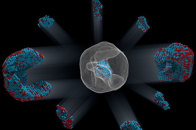
To explore how the various arrangements of atoms affect the nanoparticle’s magnetic properties, scientists from DOE’s Oak Ridge National Laboratory ran computer calculations on the Titan supercomputer at ORNL–using the coordinates and chemical type of each atom–to simulate the nanoparticle’s behavior in a magnetic field. This allowed the scientists to see patterns of atoms that are very magnetic, which is ideal for hard drives. They also saw patterns with poor magnetic properties that could sap a hard drive’s performance.

“This could help scientists learn how to steer the growth of iron-platinum nanoparticles so they develop more highly magnetic patterns of atoms,” says Ercius.

Adds Scott, “More broadly, the imaging technique will shed light on the nucleation and growth of ordered phases within nanoparticles, which isn’t fully theoretically understood but is critically important to several scientific disciplines and technologies.”

The folks at the Berkeley Lab have created a video (notice where the still image from the beginning of this post appears),

The Oak Ridge National Laboratory (ORNL), not wanting to be left out, has been mentioned in a Feb. 3, 2017 news item on ScienceDaily,

… researchers working with magnetic nanoparticles at the University of California, Los Angeles (UCLA), and the US Department of Energy’s (DOE’s) Lawrence Berkeley National Laboratory (Berkeley Lab) approached computational scientists at DOE’s Oak Ridge National Laboratory (ORNL) to help solve a unique problem: to model magnetism at the atomic level using experimental data from a real nanoparticle.

“These types of calculations have been done for ideal particles with ideal crystal structures but not for real particles,” said Markus Eisenbach, a computational scientist at the Oak Ridge Leadership Computing Facility (OLCF), a DOE Office of Science User Facility located at ORNL.

A Feb. 2, 2017 ORNL news release on EurekAlert, which originated the news item, elucidates further on how their team added to the research,

Eisenbach develops quantum mechanical electronic structure simulations that predict magnetic properties in materials. Working with Paul Kent, a computational materials scientist at ORNL’s Center for Nanophase Materials Sciences, the team collaborated with researchers at UCLA and Berkeley Lab’s Molecular Foundry to combine world-class experimental data with world-class computing to do something new–simulate magnetism atom by atom in a real nanoparticle.

Using the new data from the research teams on the West Coast, Eisenbach and Kent were able to precisely model the measured atomic structure, including defects, from a unique iron-platinum (FePt) nanoparticle and simulate its magnetic properties on the 27-petaflop Titan supercomputer at the OLCF.

Electronic structure codes take atomic and chemical structure and solve for the corresponding magnetic properties. However, these structures are typically derived from many 2-D electron microscopy or x-ray crystallography images averaged together, resulting in a representative, but not true, 3-D structure.

“In this case, researchers were able to get the precise 3-D structure for a real particle,” Eisenbach said. “The UCLA group has developed a new experimental technique where they can tell where the atoms are–the coordinates–and the chemical resolution, or what they are — iron or platinum.”

The ORNL news release goes on to describe the work from the perspective of the people who ran the supercompute simulationsr,

A Supercomputing Milestone

Magnetism at the atomic level is driven by quantum mechanics — a fact that has shaken up classical physics calculations and called for increasingly complex, first-principle calculations, or calculations working forward from fundamental physics equations rather than relying on assumptions that reduce computational workload.

For magnetic recording and storage devices, researchers are particularly interested in magnetic anisotropy, or what direction magnetism favors in an atom.

“If the anisotropy is too weak, a bit written to the nanoparticle might flip at room temperature,” Kent said.

To solve for magnetic anisotropy, Eisenbach and Kent used two computational codes to compare and validate results.

To simulate a supercell of about 1,300 atoms from strongly magnetic regions of the 23,000-atom nanoparticle, they used the Linear Scaling Multiple Scattering (LSMS) code, a first-principles density functional theory code developed at ORNL.

“The LSMS code was developed for large magnetic systems and can tackle lots of atoms,” Kent said.

As principal investigator on 2017, 2016, and previous INCITE program awards, Eisenbach has scaled the LSMS code to Titan for a range of magnetic materials projects, and the in-house code has been optimized for Titan’s accelerated architecture, speeding up calculations more than 8 times on the machine’s GPUs. Exceptionally capable of crunching large magnetic systems quickly, the LSMS code received an Association for Computing Machinery Gordon Bell Prize in high-performance computing achievement in 1998 and 2009, and developments continue to enhance the code for new architectures.

Working with Renat Sabirianov at the University of Nebraska at Omaha, the team also ran VASP, a simulation package that is better suited for smaller atom counts, to simulate regions of about 32 atoms.

“With both approaches, we were able to confirm that the local VASP results were consistent with the LSMS results, so we have a high confidence in the simulations,” Eisenbach said.

Computer simulations revealed that grain boundaries have a strong effect on magnetism. “We found that the magnetic anisotropy energy suddenly transitions at the grain boundaries. These magnetic properties are very important,” Miao said.

In the future, researchers hope that advances in computing and simulation will make a full-particle simulation possible — as first-principles calculations are currently too intensive to solve small-scale magnetism for regions larger than a few thousand atoms.

Also, future simulations like these could show how different fabrication processes, such as the temperature at which nanoparticles are formed, influence magnetism and performance.

“There’s a hope going forward that one would be able to use these techniques to look at nanoparticle growth and understand how to optimize growth for performance,” Kent said.

Finally, here’s a link to and a citation for the paper,

Deciphering chemical order/disorder and material properties at the single-atom level by Yongsoo Yang, Chien-Chun Chen, M. C. Scott, Colin Ophus, Rui Xu, Alan Pryor, Li Wu, Fan Sun, Wolfgang Theis, Jihan Zhou, Markus Eisenbach, Paul R. C. Kent, Renat F. Sabirianov, Hao Zeng, Peter Ercius, & Jianwei Miao. Nature 542, 75–79 (02 February 2017) doi:10.1038/nature21042 Published online 01 February 2017

This paper is behind a paywall.

Pushing efficiency of perovskite-based solar cells to 31%

This atomic force microscopy image of the grainy surface of a perovskite solar cell reveals a new path to much greater efficiency. Individual grains are outlined in black, low-performing facets are red, and high-performing facets are green. A big jump in efficiency could possibly be obtained if the material can be grown so that more high-performing facets develop. (Credit: Berkeley Lab)

This atomic force microscopy image of the grainy surface of a perovskite solar cell reveals a new path to much greater efficiency. Individual grains are outlined in black, low-performing facets are red, and high-performing facets are green. A big jump in efficiency could possibly be obtained if the material can be grown so that more high-performing facets develop. (Credit: Berkeley Lab)

It’s always fascinating to observe a trend (or a craze) in science, an endeavour that outsiders (like me) tend to think of as impervious to such vagaries. Perovskite seems to be making its way past the trend/craze phase and moving into a more meaningful phase. From a July 4, 2016 news item on Nanowerk,

Scientists from the Department of Energy’s Lawrence Berkeley National Laboratory (Berkeley Lab) have discovered a possible secret to dramatically boosting the efficiency of perovskite solar cells hidden in the nanoscale peaks and valleys of the crystalline material.

Solar cells made from compounds that have the crystal structure of the mineral perovskite have captured scientists’ imaginations. They’re inexpensive and easy to fabricate, like organic solar cells. Even more intriguing, the efficiency at which perovskite solar cells convert photons to electricity has increased more rapidly than any other material to date, starting at three percent in 2009 — when researchers first began exploring the material’s photovoltaic capabilities — to 22 percent today. This is in the ballpark of the efficiency of silicon solar cells.

Now, as reported online July 4, 2016 in the journal Nature Energy (“Facet-dependent photovoltaic efficiency variations in single grains of hybrid halide perovskite”), a team of scientists from the Molecular Foundry and the Joint Center for Artificial Photosynthesis, both at Berkeley Lab, found a surprising characteristic of a perovskite solar cell that could be exploited for even higher efficiencies, possibly up to 31 percent.

A July 4, 2016 Berkeley Lab news release (also on EurekAlert), which originated the news item, details the research,

Using photoconductive atomic force microscopy, the scientists mapped two properties on the active layer of the solar cell that relate to its photovoltaic efficiency. The maps revealed a bumpy surface composed of grains about 200 nanometers in length, and each grain has multi-angled facets like the faces of a gemstone.

Unexpectedly, the scientists discovered a huge difference in energy conversion efficiency between facets on individual grains. They found poorly performing facets adjacent to highly efficient facets, with some facets approaching the material’s theoretical energy conversion limit of 31 percent.

The scientists say these top-performing facets could hold the secret to highly efficient solar cells, although more research is needed.

“If the material can be synthesized so that only very efficient facets develop, then we could see a big jump in the efficiency of perovskite solar cells, possibly approaching 31 percent,” says Sibel Leblebici, a postdoctoral researcher at the Molecular Foundry.

Leblebici works in the lab of Alexander Weber-Bargioni, who is a corresponding author of the paper that describes this research. Ian Sharp, also a corresponding author, is a Berkeley Lab scientist at the Joint Center for Artificial Photosynthesis. Other Berkeley Lab scientists who contributed include Linn Leppert, Francesca Toma, and Jeff Neaton, the director of the Molecular Foundry.

A team effort

The research started when Leblebici was searching for a new project. “I thought perovskites are the most exciting thing in solar right now, and I really wanted to see how they work at the nanoscale, which has not been widely studied,” she says.

She didn’t have to go far to find the material. For the past two years, scientists at the nearby Joint Center for Artificial Photosynthesis have been making thin films of perovskite-based compounds, and studying their ability to convert sunlight and CO2 into useful chemicals such as fuel. Switching gears, they created pervoskite solar cells composed of methylammonium lead iodide. They also analyzed the cells’ performance at the macroscale.

The scientists also made a second set of half cells that didn’t have an electrode layer. They packed eight of these cells on a thin film measuring one square centimeter. These films were analyzed at the Molecular Foundry, where researchers mapped the cells’ surface topography at a resolution of ten nanometers. They also mapped two properties that relate to the cells’ photovoltaic efficiency: photocurrent generation and open circuit voltage.

This was performed using a state-of-the-art atomic force microscopy technique, developed in collaboration with Park Systems, which utilizes a conductive tip to scan the material’s surface. The method also eliminates friction between the tip and the sample. This is important because the material is so rough and soft that friction can damage the tip and sample, and cause artifacts in the photocurrent.

Surprise discovery could lead to better solar cells

The resulting maps revealed an order of magnitude difference in photocurrent generation, and a 0.6-volt difference in open circuit voltage, between facets on the same grain. In addition, facets with high photocurrent generation had high open circuit voltage, and facets with low photocurrent generation had low open circuit voltage.

“This was a big surprise. It shows, for the first time, that perovskite solar cells exhibit facet-dependent photovoltaic efficiency,” says Weber-Bargioni.

Adds Toma, “These results open the door to exploring new ways to control the development of the material’s facets to dramatically increase efficiency.”

In practice, the facets behave like billions of tiny solar cells, all connected in parallel. As the scientists discovered, some cells operate extremely well and others very poorly. In this scenario, the current flows towards the bad cells, lowering the overall performance of the material. But if the material can be optimized so that only highly efficient facets interface with the electrode, the losses incurred by the poor facets would be eliminated.

“This means, at the macroscale, the material could possibly approach its theoretical energy conversion limit of 31 percent,” says Sharp.

A theoretical model that describes the experimental results predicts these facets should also impact the emission of light when used as an LED. …

The Molecular Foundry is a DOE Office of Science User Facility located at Berkeley Lab. The Joint Center for Artificial Photosynthesis is a DOE Energy Innovation Hub led by the California Institute of Technology in partnership with Berkeley Lab.

Here’s a link to and a citation for the paper,

Facet-dependent photovoltaic efficiency variations in single grains of hybrid halide perovskite by Sibel Y. Leblebici, Linn Leppert, Yanbo Li, Sebastian E. Reyes-Lillo, Sebastian Wickenburg, Ed Wong, Jiye Lee, Mauro Melli, Dominik Ziegler, Daniel K. Angell, D. Frank Ogletree, Paul D. Ashby, Francesca M. Toma, Jeffrey B. Neaton, Ian D. Sharp, & Alexander Weber-Bargioni. Nature Energy 1, Article number: 16093 (2016  doi:10.1038/nenergy.2016.93 Published online: 04 July 2016

This paper is behind a paywall.

Dexter Johnson’s July 6, 2016 posting on his Nanoclast blog (on the IEEE [Institute of Electrical and Electronics Engineers] website} presents his take on the impact that this new finding may have,

The rise of the crystal perovskite as a potential replacement for silicon in photovoltaics has been impressive over the last decade, with its conversion efficiency improving from 3.8 to 22.1 percent over that time period. Nonetheless, there has been a vague sense that this rise is beginning to peter out of late, largely because when a solar cell made from perovskite gets larger than 1 square centimeter the best conversion efficiency had been around 15.6 percent. …

Canada has a nanotechnology industry? and an overview of the US situation

It’s always interesting to get some insight into how someone else sees the nanotechnology effort in Canada.

First, there have been two basic approaches internationally. Some countries have chosen to fund nanotechnology/nanoscience research through a national initiative/project/council/etc. Notably the US, the UK, China, and Russia, amongst others, have followed this model. For example, the US National Nanotechnology Initiative (NNI)  (a type of hub for research, communication, and commercialization efforts) has been awarded a portion of the US budget every year since 2000. The money is then disbursed through the National Science Foundation.

Canada and its nanotechnology industry efforts

By contrast, Canada has no such line item in its national budget. There is a National Institute of Nanotechnology (NINT) but it is one of many institutes that help make up Canada’s National Research Council. I’m not sure if this is still true but when it was first founded, NINT was funded in part by the federal government and in part by the province of Alberta where it is located (specifically, in Edmonton at the University of Alberta). They claim the organization has grown since its early days although it looks like it’s been shrinking. Perhaps some organizational shuffles? In any event, support for the Canadian nanotechnology efforts are more provincial than federal. Alberta (NINT and other agencies) and Québec (NanoQuébec, a provincially funded nano effort) are the standouts, with Ontario (nano Ontario, a self-organized not-for-profit group) following closely. The scene in Canada has always seemed fragmented in comparison to the countries that have nanotechnology ‘hubs’.

Patrick Johnson in a Dec. 22, 2015 article for Geopolitical Monitor offers a view which provides an overview of nanotechnology in the US and Canada,  adds to the perspective offered here, and, at times, challenges it (Note: A link has been added),

The term ‘nanotechnology’ entered into the public vernacular quite suddenly around the turn of the century, right around the same time that, when announcing the US National Nanotechnology Initiative (NNI) in 2001 [2000; see the American Association for the Advancement of Science webpage on Historical Trends in Federal R&D, scroll down to the National Nanotechnology Initiative and click on the Jpg or Excel links], President Bill Clinton declared that it would one day build materials stronger than steel, detect cancer at its inception, and store the vast records of the Library of Congress in a device the size of a sugar cube. The world of science fiction took matters even further. In his 2002 book Prey, Michael Creighton [Michael Crichton; see Wikipedia entry] wrote of a cloud of self-replicating nanorobots [also known as, nanobots or self-assemblers] that terrorize the good people of Nevada when a science experiment goes terribly wrong.

Back then the hype was palpable. Federal money was funneled to promising nanotech projects as not to fall behind in the race to master this new frontier of science. And industry analysts began to shoot for the moon in their projections. The National Science Foundation famously predicted that the nanotechnology industry would be worth $1 trillion by the year 2015.

Well here we are in 2015 and the nanotechnology market was worth around $26 billion in [sic] last year, and there hasn’t even been one case of a murderous swarm of nanomachines terrorizing the American heartland. [emphasis mine]

Is this a failure of vision? No. If anything it’s only a failure of timing.

The nanotechnology industry is still well on its way to accomplishing the goals set out at the founding of the NNI, goals which at the time sounded utterly quixotic, and this fact is increasingly being reflected in year-on-year growth numbers. In other words, nanotechnology is still a game-changer in global innovation, it’s just taking a little longer than first expected.

The Canadian Connection

Although the Canadian government is not among the world’s top spenders on nanotechnology research, the industry still represents a bright spot in the future of the Canadian economy. The public-private engine [emphasis mine] at the center of Canada’s nanotech industry, the National Institute for Nanotechnology (NINT), was founded in 2001 with the stated goal of “increasing the competitiveness of Canadian companies; creating technology solutions to meet the needs of society; expanding training programs for researchers and entrepreneurs; and enhancing Canada’s stature in the world of nanotechnology.” This ambitious mandate that NINT set out for itself was to be accomplished over the course of two broad stages: first a ‘seeding’ phase of attracting promising personnel and coordinating basic research, and the then a ‘harvesting’ phase of putting the resulting nanotechnologies to the service of Canadian industry.

Recent developments in Canadian nanotechnology [emphasis mine] show that we have already entered that second stage where the concept of nanotechnology transitions from hopeful hypothetical to real-world economic driver

I’d dearly like to know which recent developments indicate Canada’s industry has entered a serious commercialization phase. (It’s one of the shortcomings of our effort that communication is not well supported.) As well, I’d like to know more about the  “… public-private engine at the center of Canada’s nanotech industry …” as Johnson seems to be referring to the NINT, which is jointly funded (I believe) by the federal government and the province of Alberta. There is no mention of private funding on their National Research Council webpage but it does include the University of Alberta as a major supporter.

I am intrigued and I hope there is more information to come.

US and its nanotechnology industry efforts

Dr. Ambika Bumb has written a Dec. 23, 2015 article for Tech Crunch which reflects on her experience as a researcher and entrepreneur in the context of the US NNI effort and includes a plea for future NNI funding [Note: One link added and one link removed],

Indeed, I am fortunate to be the CEO of a nanomedicine technology developer that extends the hands of doctors and scientists to the cellular and molecular level.

The first seeds of interest in bringing effective nano-tools into the hands of doctors and patients were planted in my mind when I did undergrad research at Georgia Tech.  That initial interest led to me pursuing a PhD at Oxford University to develop a tri-modal nanoparticle for imaging a variety of diseases ranging from cancers to autoimmune disorders.

My graduate research only served to increase my curiosity so I then did a pair of post-doctoral fellowships at the National Cancer Institute and the National Heart Lung and Blood Institute.  When it seemed that I was a shoe-in for a life-long academic career, our technology garnered much attention and I found myself in the Bay Area founding the now award-winning Bikanta [bikanta.com].

Through the National Nanotechnology Initiative (NNI) and Nanotechnology Research and Development Act of 2003, our federal government has invested $20 billion in nanoresearch in the past 13 years.  The return on that investment has resulted in 628 agency‐to‐agency collaborations, hundreds of thousands of publications, and more than $1 trillion in revenue generated from nano‐enabled products. [emphasis mine]

Given that medical innovations take a minimum of 10 years before they translate into a clinical product, already realizing a 50X return is an astounding achievement.  Slowing down would be counter-intuitive from an academic and business perspective.

Yet, that is what is happening.  Federal funding peaked half a decade ago in 2010.  [emphasis mine] NNI investments went from $1.58B in 2010 to $1.170B in 2015 (in constant dollars), a 26% drop.  The number of nano-related papers published in the US were roughly 25 thousand in 2013, while the EU and China produced 33 and 35 thousand, respectively.

History has shown repeatedly how the United States has lost an early competitive advantage in developing high‐value technologies to international competition when commercialization infrastructure was not adequately supported.

Examples include semiconductors, advanced batteries for vehicles, and cement‐based construction materials, all of which were originally developed in the United States, but are now manufactured elsewhere.

It is now time for a second era – NNI 2.0.  A return to higher and sustained investment, the purpose of NNI 2.0 should be not just foundational research but also necessary support for rapid commercialization of nanotechnology. The translation of bench science into commercial reality requires the partnership of academic, industrial, federal, and philanthropic players.

I’m not sure why there’s a difference between Johnson’s ” … worth around $26 billion in [sic] last year …] and Bumb’s “… return on that investment has resulted … more than $1 trillion in revenue generated from nano‐enabled products.” I do know there is some controversy as to what should or should not be included when estimating the value of the ‘nanotechnology enterprise’, for example, products that are only possible due to nanotechnology as opposed to products that already existed, such as golf clubs, but are enhanced by nanotechnology.

Bumb goes on to provide a specific example from her own experience to support the plea,

When I moved from the renowned NIH [US National Institutes of Health] on the east coast to the west coast to start Bikanta, one of the highest priority concerns was how we were going to develop nanodiamond technology without access to high-end characterization instrumentation to analyze the quality of our material.  Purchasing all that equipment was not financially viable or even wise for a startup.

We were extremely lucky because our proposal was accepted by the Molecular Foundry, one of five DOE [US Department of Energy]-funded nanoscience user facilities.  While the Foundry primarily facilitates basic nanoscience projects from academic and national laboratory users, Fortune 500 companies and startups like ours also take advantage of its capabilities to answer fundamental questions and conduct proof of concept studies (~10%).

Disregarding the dynamic intellectual community for a minute, there is probably more than $150M worth of instrumentation at the Foundry.  An early startup would never be able to dream of raising a first round that large.

One of the factors of Bikanta’s success is that the Molecular Foundry enabled us to make tremendous strides in R&D in just months instead of years.  More user facilities, incubator centers, and funding for commercializing nanotech are greatly needed.

Final comments

I have to thank Dr. Bumb for pointing out that 2010 was the peak for NNI funding (see the American Association for the Advancement of Science webpage on Historical Trends in Federal R&D, scroll down to the National Nanotechnology Initiative and click on the Jpg or Excel links). I erroneously believed (although I don’t appear to have written up my belief; if you find any such statement, please let me know so I can correct it) that the 2015 US budget was the first time the NNI experienced a drop in funding.

While I found Johnson’s article interesting I wasn’t able to determine the source for his numbers and some of his material had errors that can be identified immediately, e.g., Michael Creighton instead of Michael Crichton.

SINGLE (3D Structure Identification of Nanoparticles by Graphene Liquid Cell Electron Microscopy) and the 3D structures of two individual platinum nanoparticles in solution

It seems to me there’s been an explosion of new imaging techniques lately. This one from the Lawrence Berkelely National Laboratory is all about imaging colloidal nanoparticles (nanoparticles in solution), from a July 20, 2015 news item on Azonano,

Just as proteins are one of the basic building blocks of biology, nanoparticles can serve as the basic building blocks for next generation materials. In keeping with this parallel between biology and nanotechnology, a proven technique for determining the three dimensional structures of individual proteins has been adapted to determine the 3D structures of individual nanoparticles in solution.

A multi-institutional team of researchers led by the U.S. Department of Energy (DOE)’s Lawrence Berkeley National Laboratory (Berkeley Lab), has developed a new technique called “SINGLE” that provides the first atomic-scale images of colloidal nanoparticles. SINGLE, which stands for 3D Structure Identification of Nanoparticles by Graphene Liquid Cell Electron Microscopy, has been used to separately reconstruct the 3D structures of two individual platinum nanoparticles in solution.

A July 16, 2015 Berkeley Lab news release, which originated the news item, reveals more details about the reason for the research and the research itself,

“Understanding structural details of colloidal nanoparticles is required to bridge our knowledge about their synthesis, growth mechanisms, and physical properties to facilitate their application to renewable energy, catalysis and a great many other fields,” says Berkeley Lab director and renowned nanoscience authority Paul Alivisatos, who led this research. “Whereas most structural studies of colloidal nanoparticles are performed in a vacuum after crystal growth is complete, our SINGLE method allows us to determine their 3D structure in a solution, an important step to improving the design of nanoparticles for catalysis and energy research applications.”

Alivisatos, who also holds the Samsung Distinguished Chair in Nanoscience and Nanotechnology at the University of California Berkeley, and directs the Kavli Energy NanoScience Institute at Berkeley (Kavli ENSI), is the corresponding author of a paper detailing this research in the journal Science. The paper is titled “3D Structure of Individual Nanocrystals in Solution by Electron Microscopy.” The lead co-authors are Jungwon Park of Harvard University, Hans Elmlund of Australia’s Monash University, and Peter Ercius of Berkeley Lab. Other co-authors are Jong Min Yuk, David Limmer, Qian Chen, Kwanpyo Kim, Sang Hoon Han, David Weitz and Alex Zettl.

Colloidal nanoparticles are clusters of hundreds to thousands of atoms suspended in a solution whose collective chemical and physical properties are determined by the size and shape of the individual nanoparticles. Imaging techniques that are routinely used to analyze the 3D structure of individual crystals in a material can’t be applied to suspended nanomaterials because individual particles in a solution are not static. The functionality of proteins are also determined by their size and shape, and scientists who wanted to image 3D protein structures faced a similar problem. The protein imaging problem was solved by a technique called “single-particle cryo-electron microscopy,” in which tens of thousands of 2D transmission electron microscope (TEM) images of identical copies of an individual protein or protein complex frozen in random orientations are recorded then computationally combined into high-resolution 3D reconstructions. Alivisatos and his colleagues utilized this concept to create their SINGLE technique.

“In materials science, we cannot assume the nanoparticles in a solution are all identical so we needed to develop a hybrid approach for reconstructing the 3D structures of individual nanoparticles,” says co-lead author of the Science paper Peter Ercius, a staff scientist with the National Center for Electron Microscopy (NCEM) at the Molecular Foundry, a DOE Office of Science User Facility.

“SINGLE represents a combination of three technological advancements from TEM imaging in biological and materials science,” Ercius says. “These three advancements are the development of a graphene liquid cell that allows TEM imaging of nanoparticles rotating freely in solution, direct electron detectors that can produce movies with millisecond frame-to-frame time resolution of the rotating nanocrystals, and a theory for ab initio single particle 3D reconstruction.”

The graphene liquid cell (GLC) that helped make this study possible was also developed at Berkeley Lab under the leadership of Alivisatos and co-author Zettl, a physicist who also holds joint appointments with Berkeley Lab, UC Berkeley and Kavli ENSI. TEM imaging uses a beam of electrons rather than light for illumination and magnification but can only be used in a high vacuum because molecules in the air disrupt the electron beam. Since liquids evaporate in high vacuum, samples in solutions must be hermetically sealed in special solid containers – called cells – with a very thin viewing window before being imaged with TEM. In the past, liquid cells featured silicon-based viewing windows whose thickness limited resolution and perturbed the natural state of the sample materials. The GLC developed at Berkeley lab features a viewing window made from a graphene sheet that is only a single atom thick.

“The GLC provides us with an ultra-thin covering of our nanoparticles while maintaining liquid conditions in the TEM vacuum,” Ercius says. “Since the graphene surface of the GLC is inert, it does not adsorb or otherwise perturb the natural state of our nanoparticles.”

Working at NCEM’s TEAM I, the world’s most powerful electron microscope, Ercius, Alivisatos and their colleagues were able to image in situ the translational and rotational motions of individual nanoparticles of platinum that were less than two nanometers in diameter. Platinum nanoparticles were chosen because of their high electron scattering strength and because their detailed atomic structure is important for catalysis.

“Our earlier GLC studies of platinum nanocrystals showed that they grow by aggregation, resulting in complex structures that are not possible to determine by any previously developed method,” Ercius says. “Since SINGLE derives its 3D structures from images of individual nanoparticles rotating freely in solution, it enables the analysis of heterogeneous populations of potentially unordered nanoparticles that are synthesized in solution, thereby providing a means to understand the structure and stability of defects at the nanoscale.”

The next step for SINGLE is to recover a full 3D atomic resolution density map of colloidal nanoparticles using a more advanced camera installed on TEAM I that can provide 400 frames-per-second and better image quality.

“We plan to image defects in nanoparticles made from different materials, core shell particles, and also alloys made of two different atomic species,” Ercius says. [emphasis mine]

“Two different atomic species?”, they really are pushing that biology analogy.

Here’s a link to and a citation for the paper,

3D structure of individual nanocrystals in solution by electron microscopy by Jungwon Park, Hans Elmlund, Peter Ercius, Jong Min Yuk, David T. Limme, Qian Chen, Kwanpyo Kim, Sang Hoon Han, David A. Weitz, A. Zettl, A. Paul Alivisatos. Science 17 July 2015: Vol. 349 no. 6245 pp. 290-295 DOI: 10.1126/science.aab1343

This paper is behind a paywall.

Cooling it—an application using carbon nanotubes and a theory that hotter leads to cooler

The only thing these two news items have in common is their focus on cooling down electronic devices. Well, there’s also the fact that the work is being done at the nanoscale.

First, there’s a Jan. 23, 2014 news item on Azonano about a technique using carbon nanotubes to cool down microprocessors,

“Cool it!” That’s a prime directive for microprocessor chips and a promising new solution to meeting this imperative is in the offing. Researchers with the U.S. Department of Energy (DOE)’s Lawrence Berkeley National Laboratory (Berkeley Lab) have developed a “process friendly” technique that would enable the cooling of microprocessor chips through carbon nanotubes.

Frank Ogletree, a physicist with Berkeley Lab’s Materials Sciences Division, led a study in which organic molecules were used to form strong covalent bonds between carbon nanotubes and metal surfaces. This improved by six-fold the flow of heat from the metal to the carbon nanotubes, paving the way for faster, more efficient cooling of computer chips. The technique is done through gas vapor or liquid chemistry at low temperatures, making it suitable for the manufacturing of computer chips.

The Jan. 22, 2014 Berkeley Lab news release (also on EurekAlert), which originated the news item, describes the nature  of the problem in more detail,

Overheating is the bane of microprocessors. As transistors heat up, their performance can deteriorate to the point where they no longer function as transistors. With microprocessor chips becoming more densely packed and processing speeds continuing to increase, the overheating problem looms ever larger. The first challenge is to conduct heat out of the chip and onto the circuit board where fans and other techniques can be used for cooling. Carbon nanotubes have demonstrated exceptionally high thermal conductivity but their use for cooling microprocessor chips and other devices has been hampered by high thermal interface resistances in nanostructured systems.

“The thermal conductivity of carbon nanotubes exceeds that of diamond or any other natural material but because carbon nanotubes are so chemically stable, their chemical interactions with most other materials are relatively weak, which makes for  high thermal interface resistance,” Ogletree says. “Intel came to the Molecular Foundry wanting to improve the performance of carbon nanotubes in devices. Working with Nachiket Raravikar and Ravi Prasher, who were both Intel engineers when the project was initiated, we were able to increase and strengthen the contact between carbon nanotubes and the surfaces of other materials. This reduces thermal resistance and substantially improves heat transport efficiency.”

The news release then describes the proposed solution,

Sumanjeet Kaur, lead author of the Nature Communications paper and an expert on carbon nanotubes, with assistance from co-author and Molecular Foundry chemist Brett Helms, used reactive molecules to bridge the carbon nanotube/metal interface – aminopropyl-trialkoxy-silane (APS) for oxide-forming metals, and cysteamine for noble metals. First vertically aligned carbon nanotube arrays were grown on silicon wafers, and thin films of aluminum or gold were evaporated on glass microscope cover slips. The metal films were then “functionalized” and allowed to bond with the carbon nanotube arrays. Enhanced heat flow was confirmed using a characterization technique developed by Ogletree that allows for interface-specific measurements of heat transport.

“You can think of interface resistance in steady-state heat flow as being an extra amount of distance the heat has to flow through the material,” Kaur says. “With carbon nanotubes, thermal interface resistance adds something like 40 microns of distance on each side of the actual carbon nanotube layer. With our technique, we’re able to decrease the interface resistance so that the extra distance is around seven microns at each interface.”

Although the approach used by Ogletree, Kaur and their colleagues substantially strengthened the contact between a metal and individual carbon nanotubes within an array, a majority of the nanotubes within the array may still fail to connect with the metal. The Berkeley team is now developing a way to improve the density of carbon nanotube/metal contacts. Their technique should also be applicable to single and multi-layer graphene devices, which face the same cooling issues.

For anyone who’s never heard of the Molecular Foundry before (from the news release),

The Molecular Foundry is one of five DOE [Department of Energy] Nanoscale Science Research Centers (NSRCs), national user facilities for interdisciplinary research at the nanoscale, supported by the DOE Office of Science. Together the NSRCs comprise a suite of complementary facilities that provide researchers with state-of-the-art capabilities to fabricate, process, characterize, and model nanoscale materials, and constitute the largest infrastructure investment of the National Nanotechnology Initiative. The NSRCs are located at DOE’s Argonne, Brookhaven, Lawrence Berkeley, Oak Ridge and Sandia and Los Alamos national laboratories.

My second item comes from the University of Buffalo (UB), located in the US. From a Jan. 21, 2014 University of Buffalo news release by Cory Nealon (also on EurekAlert),

Heat in electronic devices is generated by the movement of electrons through transistors, resistors and other elements of an electrical network. Depending on the network, there are a variety of ways, such as cooling fans and heat sinks, to prevent the circuits from overheating.

But as more integrated circuits and transistors are added to devices to boost their computing power, it’s becoming more difficult to keep those elements cool. Most nanoelectrics research centers are working to develop advanced materials that are capable of withstanding the extreme environment inside smartphones, laptops and other devices.

While advanced materials show tremendous potential, the UB research suggests there may still be room within the existing paradigm of electronic devices to continue developing more powerful computers.

To support their findings, the researchers fabricated nanoscale semiconductor devices in a state-of-the-art gallium arsenide crystal provided to UB by Sandia’s Reno [John L. Reno, Center for Integrated Nanotechnologies at Sandia National Laboratories]. The researchers then subjected the chip to a large voltage, squeezing an electrical current through the nanoconductors. This, in turn, increased the amount of heat circulating through the chip’s nanotransistor.

But instead of degrading the device, the nanotransistor spontaneously transformed itself into a quantum state that was protected from the effect of heating and provided a robust channel of electric current. To help explain, Bird [Jonathan Bird, UB professor of electrical engineering] offered an analogy to Niagara Falls.

“The water, or energy, comes from a source; in this case, the Great Lakes. It’s channeled into a narrow point (the Niagara River) and ultimately flows over Niagara Falls. At the bottom of waterfall is dissipated energy. But unlike the waterfall, this dissipated energy recirculates throughout the chip and changes how heat affects, or in this case doesn’t affect, the network’s operation.”

While this behavior may seem unusual, especially conceptualizing it in terms of water flowing over a waterfall, it is the direct result of the quantum mechanical nature of electronics when viewed on the nanoscale. The current is made up of electrons which spontaneously organize to form a narrow conducting filament through the nanoconductor. It is this filament that is so robust against the effects of heating.

“We’re not actually eliminating the heat, but we’ve managed to stop it from affecting the electrical network. In a way, this is an optimization of the current paradigm,” said Han [J. E. Han, UB Dept. of Physics], who developed the theoretical models which explain the findings.

What an interesting and counter-intuitive approach to managing the heat in our devices.

For those who want more, here’s a link to and citation for the carbon nanotube paper,

Enhanced thermal transport at covalently functionalized carbon nanotube array interfaces by Sumanjeet Kaur, Nachiket Raravikar, Brett A. Helms, Ravi Prasher, & D. Frank Ogletree. Nature Communications 5, Article number: 3082 doi:10.1038/ncomms4082 Published 22 January 2014

This paper is behind a paywall.

Now here’s a link to and a citation for the ‘making it hotter to make it cooler’ paper,

Formation of a protected sub-band for conduction in quantum point contacts under extreme biasing by J. Lee, J. E. Han, S. Xiao, J. Song, J. L. Reno, & J. P. Bird. Nature Nanotechnology (2014) doi:10.1038/nnano.2013.297 Published online 19 January 2014

This paper is behind a paywall although there is an option to preview it for free via ReadCube Access.