Tag Archives: Moscow Institute of Physics and Technology (MIPT)

Magnetic nanopowder for mobile 6G technology

It seems a little early to be talking about 6G technology, given that in Canada 5G technology is not fully implemented (from a February 8, 2021 article [unchanged as November 18, 2021] by Stephen Clark for whistleout.ca), Note: A link has been removed,

Should I Buy a 5G Phone Now?

There is no rush to buy a 5G phone for most Canadians. Current 5G smartphones offer other premium features such as leading edge Qualcomm CPU performance, brilliant OLED screens and recording video at 8K resolution. These devices can also cost well over $1,000, so you don’t shop for a 5G phone if that’s the only premium feature you are looking for. We expect that Canadians won’t see coast-to-coast coverage by 5G cell towers until at least 2022 [emphasis mine]. Besides, Canada’s 4G LTE mobile performance is among the fastest in the world, serves 99% of Canadians and 4G smartphones will continue to be supported for many years.

A study released by OpenSignal found Canadian 5G networks among the top 5 best in the world for mobile gaming. …

It’s good not to get too focused on one’s naval as there are many other countries in the world and it’s likely at least some, if not most, are more advanced with their 5G technology deployment and are looking forward to 6G. (See this November 1, 2021 University of Tokyo news release “Japan and Finland collaborate to develop 6G” on EurekAlert.)

Now to 6G news, this June 28, 2021 news item on phys.org describes a new technique for producing the new materials necessary for a future 6G deployment,

Material scientists have developed a fast method for producing epsilon iron oxide and demonstrated its promise for next-generation communications devices. Its outstanding magnetic properties make it one of the most coveted materials, such as for the upcoming 6G generation of communication devices and for durable magnetic recording. The work was published in the Journal of Materials Chemistry C, a journal of the Royal Society of Chemistry.

A June 23, 2021 Moscow Institute of Physics and Technology (MIPT) press release, which originated the news item, describes the work in detail,

Iron oxide (III) is one of the most widespread oxides on Earth. It is mostly found as the mineral hematite (or alpha iron oxide, α-Fe2O3). Another stable and common modification is maghemite (or gamma modification, γ-Fe2O3). The former is widely used in industry as a red pigment, and the latter as a magnetic recording medium. The two modifications differ not only in crystalline structure ( alpha-iron oxide has hexagonal syngony and gamma-iron oxide has cubic syngony) but also in magnetic properties.

In addition to these forms of iron oxide (III), there are more exotic modifications such as epsilon-, beta-, zeta-, and even glassy. The most attractive  phase is epsilon iron oxide, ε-Fe2O3. This modification has an extremely high coercive force (the ability of the material to resist an external magnetic field). The strength reaches 20 kOe at room temperature, which is comparable to the parameters of magnets based on expensive rare-earth elements. Furthermore, the material absorbs electromagnetic radiation in the sub-terahertz frequency range (100-300 GHz) through the effect of natural ferromagnetic resonance.The frequency of such resonance is one of the criteria for the use of materials in wireless communications devices – the 4G standard uses megahertz and 5G uses tens of gigahertz. There are plans to use the sub-terahertz range as a working range in the sixth generation (6G) wireless technology, which is being prepared for active introduction in our lives from the early 2030s.

The resulting material is suitable for the production of converting units or absorber circuits at these frequencies. For example, by using composite ε-Fe2O3 nanopowders it will be possible to make paints that absorb electromagnetic waves and thus shield rooms from extraneous signals, and protect signals from interception from the outside. The ε-Fe2O3 itself can also be used in 6G reception devices.

Epsilon iron oxide is an extremely rare and difficult form of iron oxide to obtain. Today, it is produced in very small quantities, with the process itself taking up to a month. This, of course, rules out its widespread application. The authors of the study developed a method for accelerated synthesis of epsilon iron oxide capable of reducing the synthesis time to one day (that is, to carry out a full cycle of more than 30 times faster!) and increasing the quantity of the resulting product. The technique is simple to reproduce, cheap and can be easily implemented in industry, and the materials required for the synthesis – iron and silicon – are among the most abundant elements on Earth.

“Although the epsilon-iron oxide phase was obtained in pure form relatively long ago, in 2004, it still has not found industrial application due to the complexity of its synthesis, for example as a medium for magnetic – recording. We have managed to simplify the technology considerably,” says Evgeny Gorbachev, a PhD student in the Department of Materials Sciences at Moscow State University and the first author of the work.

The key to successful application of materials with record-breaking characteristics is research into their fundamental physical properties. Without in-depth study, the material may be undeservedly forgotten for many years, as has happened more than once in the history of science. It was the tandem of materials scientists at Moscow State University, who synthesised the compound, and physicists at MIPT, who studied it in detail, that made the development a success.

“Materials with such high ferromagnetic resonance frequencies have enormous potential for practical applications. Today, terahertz technology is booming: it is the Internet of Things, it is ultra-fast communications, it is more narrowly focused scientific devices, and it is next-generation medical technology. While the 5G standard, which was very popular last year, operates at frequencies in the tens of gigahertz, our materials are opening the door to significantly higher frequencies (hundreds of gigahertz), which means that we are already dealing with 6G standards and higher. Now it’s up to engineers, we are happy to share the information with them and look forward to being able to hold a 6G phone in our hands,” says Dr. Liudmila Alyabyeva, Ph.D., senior researcher at the MIPT Laboratory of Terahertz Spectroscopy , where the terahertz research was carried out.

Here’s a link to and a citation for the paper,

Tuning the particle size, natural ferromagnetic resonance frequency and magnetic properties of ε-Fe2O3 nanoparticles prepared by a rapid sol–gel method by Evgeny Gorbachev, Miroslav Soshnikov, Mingxi Wu, Liudmila Alyabyeva, Dmitrii Myakishev, Ekaterina Kozlyakova, Vasilii Lebedev, Evgeny Anokhin, Boris Gorshunov, Oleg Brylev, Pavel Kazin, Lev Truso. J. Mater. Chem. C, 2021,9, 6173-6179 DOI: https://doi.org/10.1039/D1TC01242H First published 26 Apr 2021

This paper is behind a paywall.
The need for Wi-Fi speed

Yes, it’s a ‘Top Gun’ movie quote (1986) or more accurately, a paraphrasing of Tom Cruise’s line “I feel the need for speed.” I understand there’s a sequel, which is due to arrive in movie theatres or elsewhere at sometime in this decade.

Where wireless and WiFi are concerned I think there is a dog/poodle situation. ‘Dog’ is a general description where ‘poodle’ is a specific description. All poodles (specific) are dogs (general) but not all dogs are poodles. So, wireless is a general description and Wi-Fi is a specific type of wireless communication. All WiFi is wireless but not all wireless is Wi-Fi. That said, onto the research.

Given what seems to be an insatiable desire for speed in the wireless world, the quote seems quite à propos in relation to the latest work on quantum tunneling and its impact on Wi-Fi speed from the Moscow Institute of Physics and Technology (from a February 3, 2021 news item on phys.org,

Scientists from MIPT (Moscow Institute of Physics and Technology), Moscow Pedagogical State University and the University of Manchester have created a highly sensitive terahertz detector based on the effect of quantum-mechanical tunneling in graphene. The sensitivity of the device is already superior to commercially available analogs based on semiconductors and superconductors, which opens up prospects for applications of the graphene detector in wireless communications, security systems, radio astronomy, and medical diagnostics. The research results are published in Nature Communications.

A February 3, 2021 MIPT press release (also on EurekAlert), which originated the news item, provides more technical detail about the work and its relation WiFi,

Information transfer in wireless networks is based on transformation of a high-frequency continuous electromagnetic wave into a discrete sequence of bits. This technique is known as signal modulation. To transfer the bits faster, one has to increase the modulation frequency. However, this requires synchronous increase in carrier frequency. A common FM-radio transmits at frequencies of hundred megahertz, a Wi-Fi receiver uses signals of roughly five gigahertz frequency, while the 5G mobile networks can transmit up to 20 gigahertz signals. This is far from the limit, and further increase in carrier frequency admits a proportional increase in data transfer rates. Unfortunately, picking up signals with hundred gigahertz frequencies and higher is an increasingly challenging problem.

A typical receiver used in wireless communications consists of a transistor-based amplifier of weak signals and a demodulator that rectifies the sequence of bits from the modulated signal. This scheme originated in the age of radio and television, and becomes inefficient at frequencies of hundreds of gigahertz desirable for mobile systems. The fact is that most of the existing transistors aren’t fast enough to recharge at such a high frequency.

An evolutionary way to solve this problem is just to increase the maximum operation frequency of a transistor. Most specialists in the area of nanoelectronics work hard in this direction. A revolutionary way to solve the problem was theoretically proposed in the beginning of 1990’s by physicists Michael Dyakonov and Michael Shur, and realized, among others, by the group of authors in 2018. It implies abandoning active amplification by transistor, and abandoning a separate demodulator. What’s left in the circuit is a single transistor, but its role is now different. It transforms a modulated signal into bit sequence or voice signal by itself, due to non-linear relation between its current and voltage drop.

In the present work, the authors have proved that the detection of a terahertz signal is very efficient in the so-called tunneling field-effect transistor. To understand its work, one can just recall the principle of an electromechanical relay, where the passage of current through control contacts leads to a mechanical connection between two conductors and, hence, to the emergence of current. In a tunneling transistor, applying voltage to the control contact (termed as ”gate”) leads to alignment of the energy levels of the source and channel. This also leads to the flow of current. A distinctive feature of a tunneling transistor is its very strong sensitivity to control voltage. Even a small “detuning” of energy levels is enough to interrupt the subtle process of quantum mechanical tunneling. Similarly, a small voltage at the control gate is able to “connect” the levels and initiate the tunneling current

“The idea of ??a strong reaction of a tunneling transistor to low voltages is known for about fifteen years,” says Dr. Dmitry Svintsov, one of the authors of the study, head of the laboratory for optoelectronics of two-dimensional materials at the MIPT center for photonics and 2D materials. “But it’s been known only in the community of low-power electronics. No one realized before us that the same property of a tunneling transistor can be applied in the technology of terahertz detectors. Georgy Alymov (co-author of the study) and I were lucky to work in both areas. We realized then: if the transistor is opened and closed at a low power of the control signal, then it should also be good in picking up weak signals from the ambient surrounding. “

The created device is based on bilayer graphene, a unique material in which the position of energy levels (more strictly, the band structure) can be controlled using an electric voltage. This allowed the authors to switch between classical transport and quantum tunneling transport within a single device, with just a change in the polarities of the voltage at the control contacts. This possibility is of extreme importance for an accurate comparison of the detecting ability of a classical and quantum tunneling transistor.

The experiment showed that the sensitivity of the device in the tunnelling mode is few orders of magnitude higher than that in the classical transport mode. The minimum signal distinguishable by the detector against the noisy background already competes with that of commercially available superconducting and semiconductor bolometers. However, this is not the limit – the sensitivity of the detector can be further increased in “cleaner” devices with a low concentration of residual impurities. The developed detection theory, tested by the experiment, shows that the sensitivity of the “optimal” detector can be a hundred times higher.

“The current characteristics give rise to great hopes for the creation of fast and sensitive detectors for wireless communications,” says the author of the work, Dr. Denis Bandurin. And this area is not limited to graphene and is not limited to tunnel transistors. We expect that, with the same success, a remarkable detector can be created, for example, based on an electrically controlled phase transition. Graphene turned out to be just a good launching pad here, just a door, behind which is a whole world of exciting new research.”

The results presented in this paper are an example of a successful collaboration between several research groups. The authors note that it is this format of work that allows them to obtain world-class scientific results. For example, earlier, the same team of scientists demonstrated how waves in the electron sea of ??graphene can contribute to the development of terahertz technology. “In an era of rapidly evolving technology, it is becoming increasingly difficult to achieve competitive results.” – comments Dr. Georgy Fedorov, deputy head of the nanocarbon materials laboratory, MIPT, – “Only by combining the efforts and expertise of several groups can we successfully realize the most difficult tasks and achieve the most ambitious goals, which we will continue to do.”

Here’s a link to and a citation for the latest paper,

Tunnel field-effect transistors for sensitive terahertz detection by I. Gayduchenko, S. G. Xu, G. Alymov, M. Moskotin, I. Tretyakov, T. Taniguchi, K. Watanabe, G. Goltsman, A. K. Geim, G. Fedorov, D. Svintsov & D. A. Bandurin. Nature Communications volume 12, Article number: 543 (2021) DOI: https://doi.org/10.1038/s41467-020-20721-z Published: 22 January 2021

This paper is open access.

One last comment, I’m assuming since the University of Manchester is mentioned that A. K. Geim is Sir Andre K. Geim (you can look him up here is you’re not familiar with his role in the graphene research community).

Second order memristor

I think this is my first encounter with a second-order memristor. An August 28, 2019 news item on Nanowerk announces the research (Note: A link has been removed),

Researchers from the Moscow Institute of Physics and Technology [MIPT} have created a device that acts like a synapse in the living brain, storing information and gradually forgetting it when not accessed for a long time. Known as a second-order memristor, the new device is based on hafnium oxide and offers prospects for designing analog neurocomputers imitating the way a biological brain learns.

An August 28, 2019 MIPT press release (also on EurekAlert), which originated the news item, provides an explanation for neuromorphic computing (analog neurocomputers; brainlike computing), the difference between a first-order and second-order memristor, and an in depth view of the research,

Neurocomputers, which enable artificial intelligence, emulate the way the brain works. It stores data in the form of synapses, a network of connections between the nerve cells, or neurons. Most neurocomputers have a conventional digital architecture and use mathematical models to invoke virtual neurons and synapses.

Alternatively, an actual on-chip electronic component could stand for each neuron and synapse in the network. This so-called analog approach has the potential to drastically speed up computations and reduce energy costs.

The core component of a hypothetical analog neurocomputer is the memristor. The word is a portmanteau of “memory” and “resistor,” which pretty much sums up what it is: a memory cell acting as a resistor. Loosely speaking, a high resistance encodes a zero, and a low resistance encodes a one. This is analogous to how a synapse conducts a signal between two neurons (one), while the absence of a synapse results in no signal, a zero.

But there is a catch: In an actual brain, the active synapses tend to strengthen over time, while the opposite is true for inactive ones. This phenomenon known as synaptic plasticity is one of the foundations of natural learning and memory. It explains the biology of cramming for an exam and why our seldom accessed memories fade.

Proposed in 2015, the second-order memristor is an attempt to reproduce natural memory, complete with synaptic plasticity. The first mechanism for implementing this involves forming nanosized conductive bridges across the memristor. While initially decreasing resistance, they naturally decay with time, emulating forgetfulness.

“The problem with this solution is that the device tends to change its behavior over time and breaks down after prolonged operation,” said the study’s lead author Anastasia Chouprik from MIPT’s Neurocomputing Systems Lab. “The mechanism we used to implement synaptic plasticity is more robust. In fact, after switching the state of the system 100 billion times, it was still operating normally, so my colleagues stopped the endurance test.”

Instead of nanobridges, the MIPT team relied on hafnium oxide to imitate natural memory. This material is ferroelectric: Its internal bound charge distribution — electric polarization — changes in response to an external electric field. If the field is then removed, the material retains its acquired polarization, the way a ferromagnet remains magnetized.

The physicists implemented their second-order memristor as a ferroelectric tunnel junction — two electrodes interlaid with a thin hafnium oxide film (fig. 1, right). The device can be switched between its low and high resistance states by means of electric pulses, which change the ferroelectric film’s polarization and thus its resistance.

“The main challenge that we faced was figuring out the right ferroelectric layer thickness,” Chouprik added. “Four nanometers proved to be ideal. Make it just one nanometer thinner, and the ferroelectric properties are gone, while a thicker film is too wide a barrier for the electrons to tunnel through. And it is only the tunneling current that we can modulate by switching polarization.”

What gives hafnium oxide an edge over other ferroelectric materials, such as barium titanate, is that it is already used by current silicon technology. For example, Intel has been manufacturing microchips based on a hafnium compound since 2007. This makes introducing hafnium-based devices like the memristor reported in this story far easier and cheaper than those using a brand-new material.

In a feat of ingenuity, the researchers implemented “forgetfulness” by leveraging the defects at the interface between silicon and hafnium oxide. Those very imperfections used to be seen as a detriment to hafnium-based microprocessors, and engineers had to find a way around them by incorporating other elements into the compound. Instead, the MIPT team exploited the defects, which make memristor conductivity die down with time, just like natural memories.

Vitalii Mikheev, the first author of the paper, shared the team’s future plans: “We are going to look into the interplay between the various mechanisms switching the resistance in our memristor. It turns out that the ferroelectric effect may not be the only one involved. To further improve the devices, we will need to distinguish between the mechanisms and learn to combine them.”

According to the physicists, they will move on with the fundamental research on the properties of hafnium oxide to make the nonvolatile random access memory cells more reliable. The team is also investigating the possibility of transferring their devices onto a flexible substrate, for use in flexible electronics.

Last year, the researchers offered a detailed description of how applying an electric field to hafnium oxide films affects their polarization. It is this very process that enables reducing ferroelectric memristor resistance, which emulates synapse strengthening in a biological brain. The team also works on neuromorphic computing systems with a digital architecture.

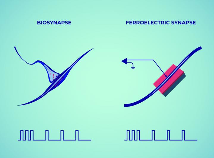
MIPT has provided this image illustrating the research,

Caption: The left image shows a synapse from a biological brain, the inspiration behind its artificial analogue (right). The latter is a memristor device implemented as a ferroelectric tunnel junction — that is, a thin hafnium oxide film (pink) interlaid between a titanium nitride electrode (blue cable) and a silicon substrate (marine blue), which doubles up as the second electrode. Electric pulses switch the memristor between its high and low resistance states by changing hafnium oxide polarization, and therefore its conductivity. Credit: Elena Khavina/MIPT Press Office

Here’s a link to and a citation for the paper,

Ferroelectric Second-Order Memristor by Vitalii Mikheev, Anastasia Chouprik, Yury Lebedinskii, Sergei Zarubin, Yury Matveyev, Ekaterina Kondratyuk, Maxim G. Kozodaev, Andrey M. Markeev, Andrei Zenkevich, Dmitrii Negrov. ACS Appl. Mater. Interfaces 2019113532108-32114 DOI: https://doi.org/10.1021/acsami.9b08189 Publication Date:August 12, 2019 Copyright © 2019 American Chemical Society

This paper is behind a paywall.

Scientometrics and science typologies

Caption: As of 2013, there were 7.8 million researchers globally, according to UNESCO. This means that 0.1 percent of the people in the world professionally do science. Their work is largely financed by governments, yet public officials are not themselves researchers. To help governments make sense of the scientific community, Russian mathematicians have devised a researcher typology. The authors initially identified three clusters, which they tentatively labeled as “leaders,” “successors,” and “toilers.” Credit: Lion_on_helium/MIPT Press Office

A June 28, 2018 Moscow Institute of Physics and Technology (MIPT; Russia) press release (also on EurekAlert) announces some intriguing research,

Researchers in various fields, from psychology to economics, build models of human behavior and reasoning to categorize people. But it does not happen as often that scientists undertake an analysis to classify their own kind.

However, research evaluation, and therefore scientist stratification as well, remain highly relevant. Six years ago, the government outlined the objective that Russian scientists should have 50 percent more publications in Web of Science- and Scopus-indexed journals. As of 2011, papers by researchers from Russia accounted for 1.66 percent of publications globally. By 2015, this number was supposed to reach 2.44%. It did grow but this has also sparked a discussion in the scientific community about the criteria used for evaluating research work.

The most common way of gauging the impact of a researcher is in terms of his or her publications. Namely, whether they are in a prestigious journal and how many times they have been cited. As with any good idea, however, one runs the risk of overdoing it. In 2005, U.S. physicist Jorge Hirsch proposed his h-index, which takes into account the number of publications by a given researcher and the number of times they have been cited. Now, scientists are increasingly doubting the adequacy of using bibliometric data as the sole independent criterion for evaluating research work. One obvious example of a flaw of this metric is that a paper can be frequently cited to point out a mistake in it.

Scientists are increasingly under pressure to publish more often. Research that might have reasonably been published in one paper is being split up into stages for separate publication. This calls for new approaches to the evaluation of work done by research groups and individual authors. Similarly, attempts to systematize the existing methods in scientometrics and stratify scientists are becoming more relevant, too. This is arguably even more important for Russia, where the research reform has been stretching for years.

One of the challenges in scientometrics is identifying the prominent types of researchers in different fields. A typology of scientists has been proposed by Moscow Institute of Physics and Technology Professor Pavel Chebotarev, who also heads the Laboratory of Mathematical Methods for Multiagent Systems Analysis at the Institute of Control Sciences of the Russian Academy of Sciences, and Ilya Vasilyev, a master’s student at MIPT.

In their paper, the two authors determined distinct types of scientists based on an indirect analysis of the style of research work, how papers are received by colleagues, and what impact they make. A further question addressed by the authors is to what degree researcher typology is affected by the scientific discipline.

“Each science has its own style of work. Publication strategies and citation practices vary, and leaders are distinguished in different ways,” says Chebotarev. “Even within a given discipline, things may be very different. This means that it is, unfortunately, not possible to have a universal system that would apply to anyone from a biologist to a philologist.”

“All of the reasonable systems that already exist are adjusted to particular disciplines,” he goes on. “They take into account the criteria used by the researchers themselves to judge who is who in their field. For example, scientists at the Institute for Nuclear Research of the Russian Academy of Sciences are divided into five groups based on what research they do, and they see a direct comparison of members of different groups as inadequate.”

The study was based on the citation data from the Google Scholar bibliographic database. To identify researcher types, the authors analyzed citation statistics for a large number of scientists, isolating and interpreting clusters of similar researchers.

Chebotarev and Vasilyev looked at the citation statistics for four groups of researchers returned by a Google Scholar search using the tags “Mathematics,” “Physics,” and “Psychology.” The first 515 and 556 search hits were considered in the case of physicists and psychologists, respectively. The authors studied two sets of mathematicians: the top 500 hits and hit Nos. 199-742. The four sets thus included frequently cited scientists from three disciplines indicating their general field of research in their profiles. Citation dynamics over each scientist’s career were examined using a range of indexes.

The authors initially identified three clusters, which they tentatively labeled as “leaders,” “successors,” and “toilers.” The leaders are experienced scientists widely recognized in their fields for research that has secured an annual citation count increase for them. The successors are young scientists who have more citations than toilers. The latter earn their high citation metrics owing to yearslong work, but they lack the illustrious scientific achievements.

Among the top 500 researchers indicating mathematics as their field of interest, 52 percent accounted for toilers, with successors and leaders making up 25.8 and 22.2 percent, respectively.

For physicists, the distribution was slightly different, with 48.5 percent of the set classified as toilers, 31.7 percent as successors, and 19.8 percent as leaders. That is, there were more successful young scientists, at the expense of leaders and toilers. This may be seen as a confirmation of the solitary nature of mathematical research, as compared with physics.

Finally, in the case of psychologists, toilers made up 47.7 percent of the set, with successors and leaders accounting for 18.3 and 34 percent. Comparing the distributions for the three disciplines investigated in the study, the authors conclude that there are more young achievers among those doing mathematical research.

A closer look enabled the authors to determine a more fine-grained cluster structure, which turned out to be remarkably similar for mathematicians and physicists. In particular, they identified a cluster of the youngest and most successful researchers, dubbed “precocious,” making up 4 percent of the mathematicians and 4.3 percent of the physicists in the set, along with the “youth” — successful researchers whose debuts were somewhat less dramatic: 29 and 31.7 percent of scientists doing math and physics research, respectively. Two further clusters were interpreted as recognized scientific authorities, or “luminaries,” and experienced researchers who have not seen an appreciable growth in the number of citations recently. Luminaries and the so-called inertia accounted for 52 and 15 percent of mathematicians and 50 and 14 percent of physicists, respectively.

There is an alternative way of clustering physicists, which recognizes a segment of researchers, who “caught the wave.” The authors suggest this might happen after joining major international research groups.

Among psychologists, 18.3 percent have been classified as precocious, though not as young as the physicists and mathematicians in the corresponding group. The most experienced and respected psychology researchers account for 22.5 percent, but there is no subdivision into luminaries and inertia, because those actively cited generally continue to be. Relatively young psychologists make up 59.2 percent of the set. The borders between clusters are relatively blurred in the case of psychology, which might be a feature of the humanities, according to the authors.

“Our pilot study showed even more similarity than we’d expected in how mathematicians and physicists are clustered,” says Chebotarev. “Whereas with psychology, things are noticeably different, yet the breakdown is slightly closer to math than physics. Perhaps, there is a certain connection between psychology and math after all, as some people say.”

“The next stage of this research features more disciplines. Hopefully, we will be ready to present the new results soon,” he concludes.

I think that they are attempting to create a new way of measuring scientific progress (scientometrics) by establishing a more representative means of measuring individual contributions based on the analysis they provide of the ways in which these ‘typologies’ are expressed across various disciplines.

For anyone who wants to investigate further, you will need to be able to read Russian. You can download the paper from here on MathNet.ru,.

Here’s my best attempt at a citation for the paper,

Making a typology of scientists on the basis of bibliometric data by I. Vasilyev, P. Yu. Chebotarev. Large-scale System Control (UBS), 2018, Issue 72, Pages 138–195 (Mi ubs948)

I’m glad to see this as there is a fair degree of dissatisfaction about the current measures for scientific progress used in any number of reports on the topic. As far as I can tell, this dissatisfaction is felt internationally.

A computer that intuitively predicts a molecule’s chemical properties

First, we have emotional artificial intelligence from MIT (Massachusetts Institute of Technology) with their Kismet [emotive AI] project and now we have intuitive computers according to an Oct. 14, 2016 news item on Nanowerk,

Scientists from Moscow Institute of Physics and Technology (MIPT)’s Research Center for Molecular Mechanisms of Aging and Age-Related Diseases together with Inria research center, Grenoble, France have developed a software package called Knodle to determine an atom’s hybridization, bond orders and functional groups’ annotation in molecules. The program streamlines one of the stages of developing new drugs.

An Oct. 14, 2016 Moscow Institute of Physics and Technology press release (also on EurekAlert), which originated the news item, expands on the theme,

Imagine that you were to develop a new drug. Designing a drug with predetermined properties is called drug-design. Once a drug has entered the human body, it needs to take effect on the cause of a disease. On a molecular level this is a malfunction of some proteins and their encoding genes. In drug-design these are called targets. If a drug is antiviral, it must somehow prevent the incorporation of viral DNA into human DNA. In this case the target is viral protein. The structure of the incorporating protein is known, and we also even know which area is the most important – the active site. If we insert a molecular “plug” then the viral protein will not be able to incorporate itself into the human genome and the virus will die. It boils down to this: you find the “plug” – you have your drug.

But how can we find the molecules required? Researchers use an enormous database of substances for this. There are special programs capable of finding a needle in a haystack; they use quantum chemistry approximations to predict the place and force of attraction between a molecular “plug” and a protein. However, databases only store the shape of a substance; information about atom and bond states is also needed for an accurate prediction. Determining these states is what Knodle does. With the help of the new technology, the search area can be reduced from hundreds of thousands to just a hundred. These one hundred can then be tested to find drugs such as Reltagravir – which has actively been used for HIV prevention since 2011.

From science lessons at school everyone is used to seeing organic substances as letters with sticks (substance structure), knowing that in actual fact there are no sticks. Every stick is a bond between electrons which obeys the laws of quantum chemistry. In the case of one simple molecule, like the one in the diagram [diagram follows], the experienced chemist intuitively knows the hybridizations of every atom (the number of neighboring atoms which it is connected to) and after a few hours looking at reference books, he or she can reestablish all the bonds. They can do this because they have seen hundreds and hundreds of similar substances and know that if oxygen is “sticking out like this”, it almost certainly has a double bond. In their research, Maria Kadukova, a MIPT student, and Sergei Grudinin, a researcher from Inria research center located in Grenoble, France, decided to pass on this intuition to a computer by using machine learning.

Compare “A solid hollow object with a handle, opening at the top and an elongation at the side, at the end of which there is another opening” and “A vessel for the preparation of tea”. Both of them describe a teapot rather well, but the latter is simpler and more believable. The same is true for machine learning, the best algorithm for learning is the simplest. This is why the researchers chose to use a nonlinear support vector machines (SVM), a method which has proven itself in recognizing handwritten text and images. On the input it was given the positions of neighboring atoms and on the output collected hybridization.

Good learning needs a lot of examples and the scientists did this using 7605 substances with known structures and atom states. “This is the key advantage of the program we have developed, learning from a larger database gives better predictions. Knodle is now one step ahead of similar programs: it has a margin of error of 3.9%, while for the closest competitor this figure is 4.7%”, explains Maria Kadukova. And that is not the only benefit. The software package can easily be modified for a specific problem. For example, Knodle does not currently work with substances containing metals, because those kind of substances are rather rare. But if it turns out that a drug for Alzheimer’s is much more effective if it has metal, the only thing needed to adapt the program is a database with metallic substances. We are now left to wonder what new drug will be found to treat a previously incurable disease.

Scientists from MIPT's Research Center for Molecular Mechanisms of Aging and Age-Related Diseases together with Inria research center, Grenoble, France have developed a software package called Knodle to determine an atom's hybridization, bond orders and functional groups' annotation in molecules. The program streamlines one of the stages of developing new drugs. Credit: MIPT Press Office

Scientists from MIPT’s Research Center for Molecular Mechanisms of Aging and Age-Related Diseases together with Inria research center, Grenoble, France have developed a software package called Knodle to determine an atom’s hybridization, bond orders and functional groups’ annotation in molecules. The program streamlines one of the stages of developing new drugs. Credit: MIPT Press Office

Here’s a link to and a citation for the paper,

Knodle: A Support Vector Machines-Based Automatic Perception of Organic Molecules from 3D Coordinates by Maria Kadukova and Sergei Grudinin. J. Chem. Inf. Model., 2016, 56 (8), pp 1410–1419 DOI: 10.1021/acs.jcim.5b00512 Publication Date (Web): July 13, 2016

Copyright © 2016 American Chemical Society

This paper is behind a paywall.

Deriving graphene-like films from salt

This research comes from Russia (mostly). A July 29, 2016 news item on ScienceDaily describes a graphene-like structure derived from salt,

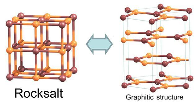
Researchers from Moscow Institute of Physics and Technology (MIPT), Skolkovo Institute of Science and Technology (Skoltech), the Technological Institute for Superhard and Novel Carbon Materials (TISNCM), the National University of Science and Technology MISiS (Russia), and Rice University (USA) used computer simulations to find how thin a slab of salt has to be in order for it to break up into graphene-like layers. Based on the computer simulation, they derived the equation for the number of layers in a crystal that will produce ultrathin films with applications in nanoelectronics. …

Caption: Transition from a cubic arrangement into several hexagonal layers. Credit: authors of the study

Caption: Transition from a cubic arrangement into several hexagonal layers. Credit: authors of the study

A July 29, 2016 Moscow Institute of Physics and Technology press release on EurekAlert, which originated the news item,  provides more technical detail,

From 3D to 2D

Unique monoatomic thickness of graphene makes it an attractive and useful material. Its crystal lattice resembles a honeycombs, as the bonds between the constituent atoms form regular hexagons. Graphene is a single layer of a three-dimensional graphite crystal and its properties (as well as properties of any 2D crystal) are radically different from its 3D counterpart. Since the discovery of graphene, a large amount of research has been directed at new two-dimensional materials with intriguing properties. Ultrathin films have unusual properties that might be useful for applications such as nano- and microelectronics.

Previous theoretical studies suggested that films with a cubic structure and ionic bonding could spontaneously convert to a layered hexagonal graphitic structure in what is known as graphitisation. For some substances, this conversion has been experimentally observed. It was predicted that rock salt NaCl can be one of the compounds with graphitisation tendencies. Graphitisation of cubic compounds could produce new and promising structures for applications in nanoelectronics. However, no theory has been developed that would account for this process in the case of an arbitrary cubic compound and make predictions about its conversion into graphene-like salt layers.

For graphitisation to occur, the crystal layers need to be reduced along the main diagonal of the cubic structure. This will result in one crystal surface being made of sodium ions Na? and the other of chloride ions Cl?. It is important to note that positive and negative ions (i.e. Na? and Cl?)–and not neutral atoms–occupy the lattice points of the structure. This generates charges of opposite signs on the two surfaces. As long as the surfaces are remote from each other, all charges cancel out, and the salt slab shows a preference for a cubic structure. However, if the film is made sufficiently thin, this gives rise to a large dipole moment due to the opposite charges of the two crystal surfaces. The structure seeks to get rid of the dipole moment, which increases the energy of the system. To make the surfaces charge-neutral, the crystal undergoes a rearrangement of atoms.

Experiment vs model

To study how graphitisation tendencies vary depending on the compound, the researchers examined 16 binary compounds with the general formula AB, where A stands for one of the four alkali metals lithium Li, sodium Na, potassium K, and rubidium Rb. These are highly reactive elements found in Group 1 of the periodic table. The B in the formula stands for any of the four halogens fluorine F, chlorine Cl, bromine Br, and iodine I. These elements are in Group 17 of the periodic table and readily react with alkali metals.

All compounds in this study come in a number of different structures, also known as crystal lattices or phases. If atmospheric pressure is increased to 300,000 times its normal value, an another phase (B2) of NaCl (represented by the yellow portion of the diagram) becomes more stable, effecting a change in the crystal lattice. To test their choice of methods and parameters, the researchers simulated two crystal lattices and calculated the pressure that corresponds to the phase transition between them. Their predictions agree with experimental data.

Just how thin should it be?

The compounds within the scope of this study can all have a hexagonal, “graphitic”, G phase (the red in the diagram) that is unstable in 3D bulk but becomes the most stable structure for ultrathin (2D or quasi-2D) films. The researchers identified the relationship between the surface energy of a film and the number of layers in it for both cubic and hexagonal structures. They graphed this relationship by plotting two lines with different slopes for each of the compounds studied. Each pair of lines associated with one compound has a common point that corresponds to the critical slab thickness that makes conversion from a cubic to a hexagonal structure energetically favourable. For example, the critical number of layers was found to be close to 11 for all sodium salts and between 19 and 27 for lithium salts.

Based on this data, the researchers established a relationship between the critical number of layers and two parameters that determine the strength of the ionic bonds in various compounds. The first parameter indicates the size of an ion of a given metal–its ionic radius. The second parameter is called electronegativity and is a measure of the ? atom’s ability to attract the electrons of element B. Higher electronegativity means more powerful attraction of electrons by the atom, a more pronounced ionic nature of the bond, a larger surface dipole, and a lower critical slab thickness.

And there’s more

Pavel Sorokin, Dr. habil., [sic] is head of the Laboratory of New Materials Simulation at TISNCM. He explains the importance of the study, ‘This work has already attracted our colleagues from Israel and Japan. If they confirm our findings experimentally, this phenomenon [of graphitisation] will provide a viable route to the synthesis of ultrathin films with potential applications in nanoelectronics.’

The scientists intend to broaden the scope of their studies by examining other compounds. They believe that ultrathin films of different composition might also undergo spontaneous graphitisation, yielding new layered structures with properties that are even more intriguing.

Here’s a link to and a citation for the paper,

Ionic Graphitization of Ultrathin Films of Ionic Compounds by A. G. Kvashnin, E. Y. Pashkin, B. I. Yakobson, and P. B. Sorokin. J. Phys. Chem. Lett., 2016, 7 (14), pp 2659–2663 DOI: 10.1021/acs.jpclett.6b01214 Publication Date (Web): June 23, 2016

Copyright © 2016 American Chemical Society

This paper is behind a paywall.

Memristor-based electronic synapses for neural networks

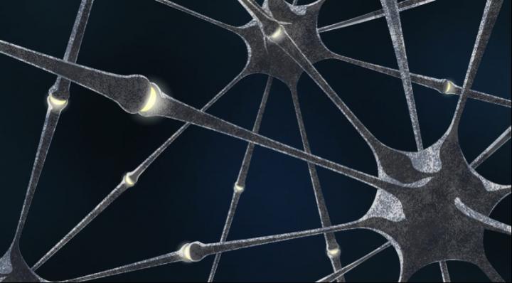
Caption: Neuron connections in biological neural networks. Credit: MIPT press office

Caption: Neuron connections in biological neural networks. Credit: MIPT press office

Russian scientists have recently published a paper about neural networks and electronic synapses based on ‘thin film’ memristors according to an April 19, 2016 news item on Nanowerk,

A team of scientists from the Moscow Institute of Physics and Technology (MIPT) have created prototypes of “electronic synapses” based on ultra-thin films of hafnium oxide (HfO2). These prototypes could potentially be used in fundamentally new computing systems.

An April 20, 2016 MIPT press release (also on EurekAlert), which originated the news item (the date inconsistency likely due to timezone differences) explains the connection between thin films and memristors,

The group of researchers from MIPT have made HfO2-based memristors measuring just 40×40 nm2. The nanostructures they built exhibit properties similar to biological synapses. Using newly developed technology, the memristors were integrated in matrices: in the future this technology may be used to design computers that function similar to biological neural networks.

Memristors (resistors with memory) are devices that are able to change their state (conductivity) depending on the charge passing through them, and they therefore have a memory of their “history”. In this study, the scientists used devices based on thin-film hafnium oxide, a material that is already used in the production of modern processors. This means that this new lab technology could, if required, easily be used in industrial processes.

“In a simpler version, memristors are promising binary non-volatile memory cells, in which information is written by switching the electric resistance – from high to low and back again. What we are trying to demonstrate are much more complex functions of memristors – that they behave similar to biological synapses,” said Yury Matveyev, the corresponding author of the paper, and senior researcher of MIPT’s Laboratory of Functional Materials and Devices for Nanoelectronics, commenting on the study.

The press release offers a description of biological synapses and their relationship to learning and memory,

A synapse is point of connection between neurons, the main function of which is to transmit a signal (a spike – a particular type of signal, see fig. 2) from one neuron to another. Each neuron may have thousands of synapses, i.e. connect with a large number of other neurons. This means that information can be processed in parallel, rather than sequentially (as in modern computers). This is the reason why “living” neural networks are so immensely effective both in terms of speed and energy consumption in solving large range of tasks, such as image / voice recognition, etc.

Over time, synapses may change their “weight”, i.e. their ability to transmit a signal. This property is believed to be the key to understanding the learning and memory functions of thebrain.

From the physical point of view, synaptic “memory” and “learning” in the brain can be interpreted as follows: the neural connection possesses a certain “conductivity”, which is determined by the previous “history” of signals that have passed through the connection. If a synapse transmits a signal from one neuron to another, we can say that it has high “conductivity”, and if it does not, we say it has low “conductivity”. However, synapses do not simply function in on/off mode; they can have any intermediate “weight” (intermediate conductivity value). Accordingly, if we want to simulate them using certain devices, these devices will also have to have analogous characteristics.

The researchers have provided an illustration of a biological synapse,

Fig.2 The type of electrical signal transmitted by neurons (a “spike”). The red lines are various other biological signals, the black line is the averaged signal. Source: MIPT press office

Fig.2 The type of electrical signal transmitted by neurons (a “spike”). The red lines are various other biological signals, the black line is the averaged signal. Source: MIPT press office

Now, the press release ties the memristor information together with the biological synapse information to describe the new work at the MIPT,

As in a biological synapse, the value of the electrical conductivity of a memristor is the result of its previous “life” – from the moment it was made.

There is a number of physical effects that can be exploited to design memristors. In this study, the authors used devices based on ultrathin-film hafnium oxide, which exhibit the effect of soft (reversible) electrical breakdown under an applied external electric field. Most often, these devices use only two different states encoding logic zero and one. However, in order to simulate biological synapses, a continuous spectrum of conductivities had to be used in the devices.

“The detailed physical mechanism behind the function of the memristors in question is still debated. However, the qualitative model is as follows: in the metal–ultrathin oxide–metal structure, charged point defects, such as vacancies of oxygen atoms, are formed and move around in the oxide layer when exposed to an electric field. It is these defects that are responsible for the reversible change in the conductivity of the oxide layer,” says the co-author of the paper and researcher of MIPT’s Laboratory of Functional Materials and Devices for Nanoelectronics, Sergey Zakharchenko.

The authors used the newly developed “analogue” memristors to model various learning mechanisms (“plasticity”) of biological synapses. In particular, this involved functions such as long-term potentiation (LTP) or long-term depression (LTD) of a connection between two neurons. It is generally accepted that these functions are the underlying mechanisms of  memory in the brain.

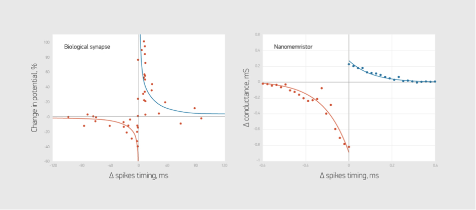
The authors also succeeded in demonstrating a more complex mechanism – spike-timing-dependent plasticity, i.e. the dependence of the value of the connection between neurons on the relative time taken for them to be “triggered”. It had previously been shown that this mechanism is responsible for associative learning – the ability of the brain to find connections between different events.

To demonstrate this function in their memristor devices, the authors purposefully used an electric signal which reproduced, as far as possible, the signals in living neurons, and they obtained a dependency very similar to those observed in living synapses (see fig. 3).

Fig.3. The change in conductivity of memristors depending on the temporal separation between "spikes"(rigth) and thr change in potential of the neuron connections in biological neural networks. Source: MIPT press office

Fig.3. The change in conductivity of memristors depending on the temporal separation between “spikes”(rigth) and thr change in potential of the neuron connections in biological neural networks. Source: MIPT press office

These results allowed the authors to confirm that the elements that they had developed could be considered a prototype of the “electronic synapse”, which could be used as a basis for the hardware implementation of artificial neural networks.

“We have created a baseline matrix of nanoscale memristors demonstrating the properties of biological synapses. Thanks to this research, we are now one step closer to building an artificial neural network. It may only be the very simplest of networks, but it is nevertheless a hardware prototype,” said the head of MIPT’s Laboratory of Functional Materials and Devices for Nanoelectronics, Andrey Zenkevich.

Here’s a link to and a citation for the paper,

Crossbar Nanoscale HfO2-Based Electronic Synapses by Yury Matveyev, Roman Kirtaev, Alena Fetisova, Sergey Zakharchenko, Dmitry Negrov and Andrey Zenkevich. Nanoscale Research Letters201611:147 DOI: 10.1186/s11671-016-1360-6

Published: 15 March 2016

This is an open access paper.

Plastic memristors for neural networks

There is a very nice explanation of memristors and computing systems from the Moscow Institute of Physics and Technology (MIPT). First their announcement, from a Jan. 27, 2016 news item on ScienceDaily,

A group of scientists has created a neural network based on polymeric memristors — devices that can potentially be used to build fundamentally new computers. These developments will primarily help in creating technologies for machine vision, hearing, and other machine sensory systems, and also for intelligent control systems in various fields of applications, including autonomous robots.

The authors of the new study focused on a promising area in the field of memristive neural networks – polymer-based memristors – and discovered that creating even the simplest perceptron is not that easy. In fact, it is so difficult that up until the publication of their paper in the journal Organic Electronics, there were no reports of any successful experiments (using organic materials). The experiments conducted at the Nano-, Bio-, Information and Cognitive Sciences and Technologies (NBIC) centre at the Kurchatov Institute by a joint team of Russian and Italian scientists demonstrated that it is possible to create very simple polyaniline-based neural networks. Furthermore, these networks are able to learn and perform specified logical operations.

A Jan. 27, 2016 MIPT press release on EurekAlert, which originated the news item, offers an explanation of memristors and a description of the research,

A memristor is an electric element similar to a conventional resistor. The difference between a memristor and a traditional element is that the electric resistance in a memristor is dependent on the charge passing through it, therefore it constantly changes its properties under the influence of an external signal: a memristor has a memory and at the same time is also able to change data encoded by its resistance state! In this sense, a memristor is similar to a synapse – a connection between two neurons in the brain that is able, with a high level of plasticity, to modify the efficiency of signal transmission between neurons under the influence of the transmission itself. A memristor enables scientists to build a “true” neural network, and the physical properties of memristors mean that at the very minimum they can be made as small as conventional chips.

Some estimates indicate that the size of a memristor can be reduced up to ten nanometers, and the technologies used in the manufacture of the experimental prototypes could, in theory, be scaled up to the level of mass production. However, as this is “in theory”, it does not mean that chips of a fundamentally new structure with neural networks will be available on the market any time soon, even in the next five years.

The plastic polyaniline was not chosen by chance. Previous studies demonstrated that it can be used to create individual memristors, so the scientists did not have to go through many different materials. Using a polyaniline solution, a glass substrate, and chromium electrodes, they created a prototype with dimensions that, at present, are much larger than those typically used in conventional microelectronics: the strip of the structure was approximately one millimeter wide (they decided to avoid miniaturization for the moment). All of the memristors were tested for their electrical characteristics: it was found that the current-voltage characteristic of the devices is in fact non-linear, which is in line with expectations. The memristors were then connected to a single neuromorphic network.

A current-voltage characteristic (or IV curve) is a graph where the horizontal axis represents voltage and the vertical axis the current. In conventional resistance, the IV curve is a straight line; in strict accordance with Ohm’s Law, current is proportional to voltage. For a memristor, however, it is not just the voltage that is important, but the change in voltage: if you begin to gradually increase the voltage supplied to the memristor, it will increase the current passing through it not in a linear fashion, but with a sharp bend in the graph and at a certain point its resistance will fall sharply.

Then if you begin to reduce the voltage, the memristor will remain in its conducting state for some time, after which it will change its properties rather sharply again to decrease its conductivity. Experimental samples with a voltage increase of 0.5V hardly allowed any current to pass through (around a few tenths of a microamp), but when the voltage was reduced by the same amount, the ammeter registered a figure of 5 microamps. Microamps are of course very small units, but in this case it is the contrast that is most significant: 0.1 μA to 5 μA is a difference of fifty times! This is more than enough to make a clear distinction between the two signals.

After checking the basic properties of individual memristors, the physicists conducted experiments to train the neural network. The training (it is a generally accepted term and is therefore written without inverted commas) involves applying electric pulses at random to the inputs of a perceptron. If a certain combination of electric pulses is applied to the inputs of a perceptron (e.g. a logic one and a logic zero at two inputs) and the perceptron gives the wrong answer, a special correcting pulse is applied to it, and after a certain number of repetitions all the internal parameters of the device (namely memristive resistance) reconfigure themselves, i.e. they are “trained” to give the correct answer.

The scientists demonstrated that after about a dozen attempts their new memristive network is capable of performing NAND logical operations, and then it is also able to learn to perform NOR operations. Since it is an operator or a conventional computer that is used to check for the correct answer, this method is called the supervised learning method.

Needless to say, an elementary perceptron of macroscopic dimensions with a characteristic reaction time of tenths or hundredths of a second is not an element that is ready for commercial production. However, as the researchers themselves note, their creation was made using inexpensive materials, and the reaction time will decrease as the size decreases: the first prototype was intentionally enlarged to make the work easier; it is physically possible to manufacture more compact chips. In addition, polyaniline can be used in attempts to make a three-dimensional structure by placing the memristors on top of one another in a multi-tiered structure (e.g. in the form of random intersections of thin polymer fibers), whereas modern silicon microelectronic systems, due to a number of technological limitations, are two-dimensional. The transition to the third dimension would potentially offer many new opportunities.

The press release goes to explain what the researchers mean when they mention a fundamentally different computer,

The common classification of computers is based either on their casing (desktop/laptop/tablet), or on the type of operating system used (Windows/MacOS/Linux). However, this is only a very simple classification from a user perspective, whereas specialists normally use an entirely different approach – an approach that is based on the principle of organizing computer operations. The computers that we are used to, whether they be tablets, desktop computers, or even on-board computers on spacecraft, are all devices with von Neumann architecture; without going into too much detail, they are devices based on independent processors, random access memory (RAM), and read only memory (ROM).

The memory stores the code of a program that is to be executed. A program is a set of instructions that command certain operations to be performed with data. Data are also stored in the memory* and are retrieved from it (and also written to it) in accordance with the program; the program’s instructions are performed by the processor. There may be several processors, they can work in parallel, data can be stored in a variety of ways – but there is always a fundamental division between the processor and the memory. Even if the computer is integrated into one single chip, it will still have separate elements for processing information and separate units for storing data. At present, all modern microelectronic systems are based on this particular principle and this is partly the reason why most people are not even aware that there may be other types of computer systems – without processors and memory.

*) if physically different elements are used to store data and store a program, the computer is said to be built using Harvard architecture. This method is used in certain microcontrollers, and in small specialized computing devices. The chip that controls the function of a refrigerator, lift, or car engine (in all these cases a “conventional” computer would be redundant) is a microcontroller. However, neither Harvard, nor von Neumann architectures allow the processing and storage of information to be combined into a single element of a computer system.

However, such systems do exist. Furthermore, if you look at the brain itself as a computer system (this is purely hypothetical at the moment: it is not yet known whether the function of the brain is reducible to computations), then you will see that it is not at all built like a computer with von Neumann architecture. Neural networks do not have a specialized computer or separate memory cells. Information is stored and processed in each and every neuron, one element of the computer system, and the human brain has approximately 100 billion of these elements. In addition, almost all of them are able to work in parallel (simultaneously), which is why the brain is able to process information with great efficiency and at such high speed. Artificial neural networks that are currently implemented on von Neumann computers only emulate these processes: emulation, i.e. step by step imitation of functions inevitably leads to a decrease in speed and an increase in energy consumption. In many cases this is not so critical, but in certain cases it can be.

Devices that do not simply imitate the function of neural networks, but are fundamentally the same could be used for a variety of tasks. Most importantly, neural networks are capable of pattern recognition; they are used as a basis for recognising handwritten text for example, or signature verification. When a certain pattern needs to be recognised and classified, such as a sound, an image, or characteristic changes on a graph, neural networks are actively used and it is in these fields where gaining an advantage in terms of speed and energy consumption is critical. In a control system for an autonomous flying robot every milliwatt-hour and every millisecond counts, just in the same way that a real-time system to process data from a collider detector cannot take too long to “think” about highlighting particle tracks that may be of interest to scientists from among a large number of other recorded events.

Bravo to the writer!

Here’s a link to and a citation for the paper,

Hardware elementary perceptron based on polyaniline memristive devices by V.A. Demin. V. V. Erokhin, A.V. Emelyanov, S. Battistoni, G. Baldi, S. Iannotta, P.K. Kashkarov, M.V. Kovalchuk. Organic Electronics Volume 25, October 2015, Pages 16–20 doi:10.1016/j.orgel.2015.06.015

This paper is behind a paywall.