Tag Archives: Nagoya University

Quick and efficient nanographene synthesis

Thank you to Nagoya University (Japan) for making this image available.

Caption: APEX reactions are carried out on the K, M and bay regions of the polycyclic aromatic hydrocarbon, synthesizing multiple nanographenes. These reactions can then be repeated, further increasing the number of potential nanographene structures that can be synthesized. Credit: Issey Takahashi

From a June 28, 2021 Nagoya University press release (also on EurekAlert),

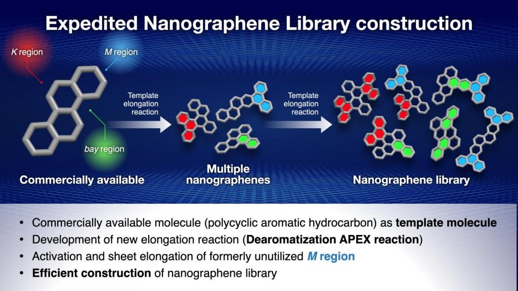
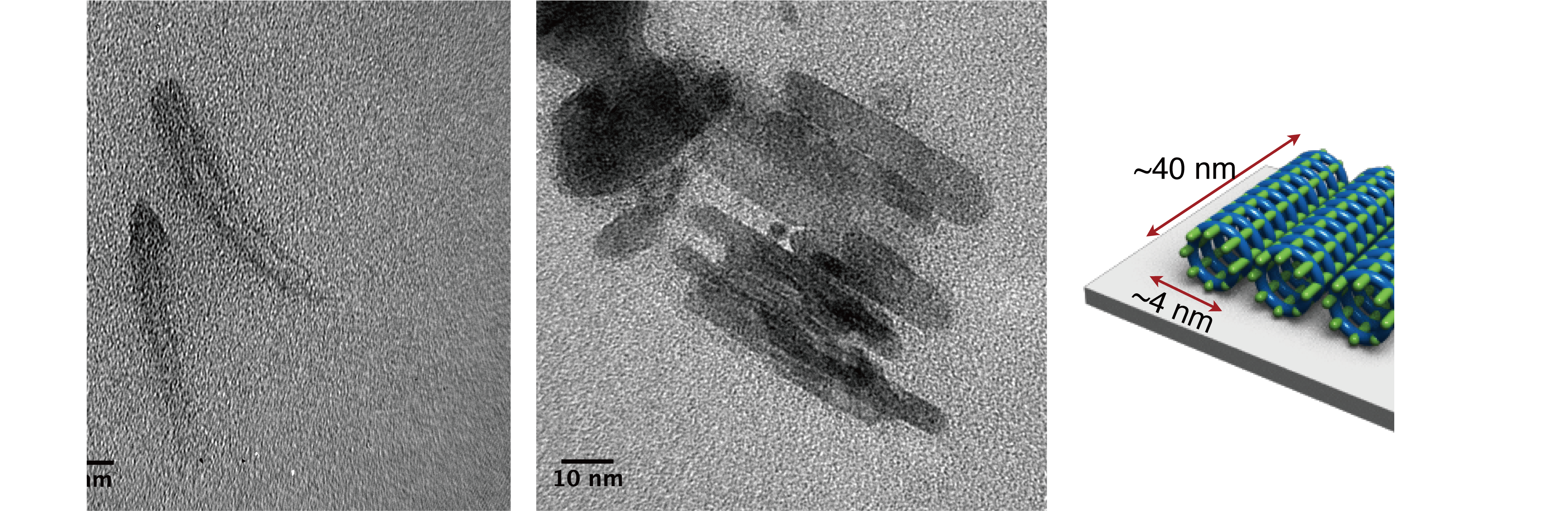
A group of researchers at Nagoya University, Japan, have developed a new method for quickly and efficiently synthesizing nanographenes, a type of nanocarbon with great potential as a next generation material.

Nanographenes are the part structures of graphene, which is a sheet of carbon atoms around 3 nanometers thick with particular potential for use in semiconductor development, having electron mobility several hundred times better than current generation materials. Graphene was first isolated in 2004, a discovery which received the 2010 Nobel Prize in physics, making it a very new material which is currently the subject of a great deal of research.

With magnetic and electric characteristics beyond those of graphene, nanographenes are equally of interest to scientists in the nanocarbon research field. The biggest obstacle, albeit an exciting one, faced by researchers is the sheer number of potential nanographenes. The number of potentially possible nanographene structures increases with the number of benzene rings (6 atoms of carbon in a hexagonal formation) to make them. For example, even a relatively small 10 benzene ring nanographene may have up to 16,000 variants. As each nanographene has different physical characteristics, the key to applied nanographene research is to identify the relationship between the structure and characteristics of as many nanographenes as possible.

Thus, scientists’ task is to create a nanographene library, containing data on the properties of as many nanographenes as possible. However, the current method of nanographene synthesis, known as a coupling reaction, is a multi-step process which produces one single nanographene. Thus, to create a 100-nanographene library, 100 separate coupling reactions would have to be carried out. Even this would be a significant undertaking, rendering the construction of a truly comprehensive nanographene library practically impossible.

To solve this problem, the Nagoya University research group, led by Professor Kenichiro Itami, have been working on the APEX reaction, a reaction which uses polycyclic aromatic hydrocarbons as templates to synthesize nanographenes. Polycyclic aromatic hydrocarbons have three areas of their structure – known as the K region, M region and bay region – which can be elongated in an APEX reaction, producing three nanographenes. These nanographenes can then be further elongated in a second reaction, meaning that a large number of nanographenes can be synthesized from a single polycyclic aromatic hydrocarbon template molecule.

With Professor Itami’s group having already developed the K region APEX reaction, and another group of scientists having done so for the bay region, they turned their attention to the M region. They activated the M region using the 1950 Nobel Prize winning Diels-Alder reaction, and succeeded in carrying out an elongation reaction on the activated M region, thus rendering all three possible sites on the polycyclic aromatic hydrocarbons capable of synthesizing nanographenes.

The researchers were able to produce 13 nanographenes with three APEX reactions, with most of these being previously unseen structures, thus proving both the efficiency and usefulness of this new method.

This exciting new piece of research and its potential to accelerate the creation of nanographene libraries is a step towards the development of the next generation of materials, which have the potential to revolutionize semiconductors and solar energy and improve lives all around the world.

Here’s a link to and a citation for the paper,

Diversity-oriented synthesis of nanographenes enabled by dearomative annulative π-extension by Wataru Matsuoka, Hideto Ito, David Sarlah & Kenichiro Itami. Nature Communications volume 12, Article number: 3940 (2021) DOI: https://doi.org/10.1038/s41467-021-24261-y Published 24 June 2021

This paper is open access.

Purifying carbon nanotubes with dietary fiber

This work comes out of Japan according to a November 2, 2019 news item on Nanowerk,

A new, cheaper method easily and effectively separates two types of carbon nanotubes. The process, developed by Nagoya University researchers in Japan, could be up-scaled for manufacturing purified batches of single-wall carbon nanotubes that can be used in high-performance electronic devices.

Single-wall carbon nanotubes (SWCNTs) have excellent electronic and mechanical properties, making them ideal candidates for use in a wide range of electronic devices, including the thin-film transistors found in LCD displays. A problem is that only two-thirds of manufactured SWCNTs are suitable for use in electronic devices. The useful semiconducting SWCNTs must be separated from the unwanted metallic ones. But the most powerful purification process, known as aqueous two-phase extraction, currently involves the use of a costly polysaccharide, called dextran.

Caption: The unwanted metallic SWCNTs deposited at the bottom of the solution, while the wanted semiconducting ones floated to the top. Credit: Haruka Omachi

An October 29, 2019 Nagoya University press release (also on EurekAlert but dated Nov. 2, 2019), which originated the news item, describes how dextran could be replaced with something much cheaper in the SWCNT purification process,

Organic chemist Haruka Omachi and colleagues at Nagoya University hypothesized that dextran’s effectiveness in separating semiconducting from metallic SWCNTs lies in the linkages connecting its glucose units. Instead of using dextran to separate the two types of SWCNTs, the team tried the significantly cheaper isomaltodextran, which has many more of these linkages.

A batch of SWCNTs was left for 15 minutes in a solution containing polyethylene glycol and isomaltodextrin and then centrifuged for five minutes. Three different types of isomaltodextrin were tried, each with a different number of linkages and a different molecular weight. The team found that metallic SWCNTs separated to the bottom isomaltodextrin part of the solution, while the semiconducting SWCNTs floated to the top polyethylene glycol part.

The type of isomaltodextrin with high molecular weight and the most linkages was the most (99%) effective in separating the two types of SWCNTs. The team also found that another polysaccharide, called pullulan, whose glucose units are connected with different kinds of linkages, was ineffective in separating the two types of SWCNTs. The researchers suggest that the number and type of linkages present in isomaltodextrin play an important role in their ability to effectively separate the carbon nanotubes.

The team also found that a thin-film transistor made with their purified semiconducting SWCNTs performed very well.

Isomaltodextrin is a cheap and widely available polysaccharide produced from starch that is used as a dietary fibre. This makes it a cost-effective alternative for the SWCNT extraction process. Omachi and his colleagues are currently in discussions with companies to commercialize their approach. They are also working on improving the performance of thin-film transistors using semiconducting SWCNTs in flexible displays and sensor devices.

Here’s a link to and a citation for the paper,

Aqueous two-phase extraction of semiconducting single-wall carbon nanotubes with isomaltodextrin and thin-film transistor applications by Haruka Omachi, Tomohiko Komuro, Kaisei Matsumoto, Minako Nakajima, Hikaru Watanabe, Jun Hirotani, Yutaka Ohno, and Hisanori Shinohara. Applied Physics Express, Volume 12, Number 9 DOI: https://doi.org/10.7567/1882-0786/ab369 Published 14 August 2019 • © 2019 The Japan Society of Applied Physics

This paper is open access.

The latest ‘golden’ age for electronics

I don’t know the dates for the last ‘golden’ age of electronics but I can certainly understand why these Japanese researchers are excited about their work. In any event, I think the ‘golden age’ is more of a play on words. From a June 25, 2019 news item on Nanowerk (Note: A link has been removed),

One way that heat damages electronic equipment is it makes components expand at different rates, resulting in forces that cause micro-cracking and distortion. Plastic components and circuit boards are particularly prone to damage due to changes in volume during heating and cooling cycles. But if a material could be incorporated into the components that compensates for the expansion, the stresses would be reduced and their lifetime increased.

Everybody knows one material that behaves like this: liquid water expands when it freezes and ice contracts when it melts. But liquid water and electronics don’t mix well – instead, what’s needed is a solid with “negative thermal expansion” (NTE).

Although such materials have been known since the 1960s, a number of challenges had to be overcome before the concept would be broadly useful and commercially viable. In terms of both materials and function, these efforts have only had limited success.

The experimental materials had been produced under specialized laboratory conditions using expensive equipment; and even then, the temperature and pressure ranges in which they would exhibit NTE were well outside normal everyday conditions.

Moreover, the amount they expanded and contracted depended on the direction, which induced internal stresses that changed their structure, meaning that the NTE property would not last longer than a few heating and cooling cycles.

A research team led by Koshi Takenaka of Nagoya University has succeeded in overcoming these materials-engineering challenges (APL Materials, “Valence fluctuations and giant isotropic negative thermal expansion in Sm1–xRxS (R = Y, La, Ce, Pr, Nd)”).

A June 22, 2019 Nagoya University press release (also on EurekAlert but published on June 25, 2019), which originated the news item, provides more technical detail,

Inspired by the series of work by Noriaki Sato, also of Nagoya University – whose discovery last year of superconductivity in quasicrystals was considered one of the top ten physics discoveries of the year by Physics World magazine – Professor Takenaka took the rare earth element samarium and its sulfide, samarium monosulfide (SmS), which is known to change phase from the “black phase” to the smaller-volume “golden phase”. The problem was to tune the range of temperatures at which the phase transition occurs. The team’s solution was to replace a small proportion of samarium atoms with another rare earth element, giving Sm1-xRxS, where “R” is any one of the rare earth elements cerium (Ce), neodymium (Nd), praseodymium (Pr) or yttrium (Y). The fraction x the team used was typically 0.2, except for yttrium. These materials showed “giant negative thermal expansion” of up to 8% at ordinary room pressure and a useful range of temperatures (around 150 degrees) including at room temperature and above … . Cerium is the star candidate here because it is relatively cheap.

The nature of the phase transition is such that the materials can be powdered into very small crystal sizes around a micron on a side without losing their negative expansion property. This broadens the industrial applications, particularly within electronics.

While the Nagoya University group’s engineering achievement is impressive, how the negative expansion works is fascinating from a fundamental physics viewpoint. During the black-golden transition, the crystal structure stays the same but the atoms get closer together: the unit cell size becomes smaller because (as is very likely but perhaps not yet 100% certain) the electron structure of the samarium atoms changes and makes them smaller – a process of intra-atomic charge transfer called a “valence transition” or “valence fluctuation” within the samarium atoms … . “My impression,” says Professor Takenaka, “is that the correlation between the lattice volume and the electron structure of samarium is experimentally verified for this class of sulfides.”

More specifically, in the black (lower temperature) phase, the electron configuration of the samarium atoms is (4f)6, meaning that in their outermost shell they have 6 electrons in the f orbitals (with s, p and d orbitals filled); while in the golden phase the electronic configuration is (4f)5(5d)1 -an electron has moved out of a 4f orbital into a 5d orbital. Although a “higher” shell is starting to be occupied, it turns out – through a quirk of the Pauli Exclusion Principle – that the second case gives a smaller atom size, leading to a smaller crystal size and negative expansion.

But this is only part of the fundamental picture. In the black phase, samarium sulfide and its doped offshoots are insulators – they do not conduct electricity; while in the golden phase they turn into conductors (i.e. metals). This is suggesting that during the black-golden phase transition the band structure of the whole crystal is influencing the valance transition within the samarium atoms. Although nobody has done the theoretical calculations for the doped samarium sulfides made by Professor Takenaka’s group, a previous theoretical study has indicated that when electrons leave the samarium atoms’ f orbital, they leave behind a positively charged “hole” which itself interacts repulsively with holes in the crystal’s conduction band, affecting their exchange interaction. This becomes a cooperative effect that then drives the valence transition in the samarium atoms. The exact mechanism, though, is not well understood.

Nevertheless, the Nagoya University-led group’s achievement is one of engineering, not pure physics. “What is important for many engineers is the ability to use the material to reduce device failure due to thermal expansion,” explains Professor Takenaka. “In short, in a certain temperature range – the temperature range in which the intended device operates, typically an interval of dozens of degrees or more – the volume needs to gradually decrease with a rise in temperature and increase as the temperature falls. Of course, I also know that volume expansion on cooling during a phase transition [like water freezing] is a common case for many materials. However, if the volume changes in a very narrow temperature range, there is no engineering value. The present achievement is the result of material engineering, not pure physics.”

Perhaps it even heralds a new “golden” age for electronics.

I worked in a company for a data communications company that produced hardware and network management software. From a hardware perspective, heat was an enemy which distorted your circuit boards and cost you significant money not only for replacements but also when you included fans to keep the equipment cool (or as cool as possible).

Enough with the reminiscences, here’s a link to and a citation for the paper,

Valence fluctuations and giant isotropic negative thermal expansion in Sm1–xRxS (R = Y, La, Ce, Pr, Nd) by D. Asai, Y. Mizuno, H. Hasegawa, Y. Yokoyama, Y. Okamoto, N. Katayama, H. S. Suzuki, Y. Imanaka, and K. Takenaka. Applied Physics Letters > Volume 114, Issue 14 > 10.1063/1.5090546 or Appl. Phys. Lett. 114, 141902 (2019); https://doi.org/10.1063/1.5090546. Published Online: 12 April 2019

This paper is behind a paywall.

Stellar’s jay gives structural colo(u)r a new look

The structural colo(u)r stories I’ve posted previously identify nanostructures as the reason for why certain animals and plants display a particular set of optical properties, colours that can’t be obtained by pigment or dye. However, the Stellar’s jay structural colour story is a little different.

Caption: Bio-inspired bright structurally colored colloidal amorphous array enhanced by controlling thickness and black background. ©Yukikazu Takeoka

From a May 8, 2017 news item on ScienceDaily,

A Nagoya University-led [Japan] research team mimics the rich color of bird plumage and demonstrates new ways to control how light interacts with materials.

Bright colors in the natural world often result from tiny structures in feathers or wings that change the way light behaves when it’s reflected. So-called “structural color” is responsible for the vivid hues of birds and butterflies. Artificially harnessing this effect could allow us to engineer new materials for applications such as solar cells and chameleon-like adaptive camouflage.

Inspired by the deep blue coloration of a native North American bird, Stellar’s jay, a team at Nagoya University reproduced the color in their lab, giving rise to a new type of artificial pigment. This development was reported in Advanced Materials.

“The Stellar’s jay’s feathers provide an excellent example of angle-independent structural color,” says last author Yukikazu Takeoka, “This color is enhanced by dark materials, which in this case can be attributed to black melanin particles in the feathers.

A May 8, 2017 Nagoya University press release (also on EurekAlert), which originated the news item, expands on the theme of what makes the structural colour of a Stellar’s jay feather different,

In most cases, structural colors appear to change when viewed from different perspectives. For example, imagine the way that the colors on the underside of a CD appear to shift when the disc is viewed from a different angle. The difference in Stellar’s jay’s blue is that the structures, which interfere with light, sit on top of black particles that can absorb a part of this light. This means that at all angles, however you look at it, the color of the Stellar’s Jay does not change.

The team used a “layer-by-layer” approach to build up films of fine particles that recreated the microscopic sponge-like texture and black backing particles of the bird’s feathers.

To mimic the feathers, the researchers covered microscopic black core particles with layers of even smaller transparent particles, to make raspberry-like particles. The size of the core and the thickness of the layers controlled the color and saturation of the resulting pigments. Importantly, the color of these particles did not change with viewing angle.

“Our work represents a much more efficient way to design artificially produced angle-independent structural colors,” Takeoka adds. “We still have much to learn from biological systems, but if we can understand and successfully apply these phenomena, a whole range of new metamaterials will be accessible for all kinds of advanced applications where interactions with light are important.”

Here’s a link to and a citation for the paper,

Bio-Inspired Bright Structurally Colored Colloidal Amorphous Array Enhanced by Controlling Thickness and Black Background by Masanori Iwata, Midori Teshima, Takahiro Seki, Shinya Yoshioka, and Yukikazu Takeoka. Advanced Materials DOI: 10.1002/adma.201605050 Version of Record online: 26 APR 2017

© 2017 WILEY-VCH Verlag GmbH & Co. KGaA, Weinheim

This paper is behind a paywall.

Ordinarily, I’d expect to see the term ‘nano’ somewhere in the press release or in the abstract but that’s not the case here. The best I could find was a reference to ‘submicrometer-sized .. particles” in the abstract. I suppose that could refer to the nanoscale but given that a Japanese researcher (Norio Taniguchi in 1974) coined the phrase ‘nanotechnology’ to describe research at that scale it seems unlikely that Japanese researchers some forty years later wouldn’t use that term when appropriate.

Mechanically strong organic nanotubes made with light

This research comes from Nagoya University in Japan according to an Aug. 30, 2016 news item on Nanowerk,

Organic nanotubes (ONTs) are tubular nanostructures composed of organic molecules that have unique properties and have found various applications, such as electro-conductive materials and organic photovoltaics. A group of scientists at Nagoya University have developed a simple and effective method for the formation of robust covalent ONTs from simple molecules. This method is expected to be useful in generating a range of nanotube-based materials with desirable properties.

An Aug. 30, 2016 Nagoya University press release (also on EurekAlert), which originated the news item, provides more information,

Kaho Maeda, Dr. Hideto Ito, Professor Kenichiro Itami of the JST-ERATO Itami Molecular Nanocarbon Project and the Institute of Transformative Bio-Molecules (ITbM) of Nagoya University, and their colleagues have reported in the Journal of the American Chemical Society, on the development of a new and simple strategy, “helix-to-tube” to synthesize covalent organic nanotubes.

Organic nanotubes (ONTs) are organic molecules with tubular nanostructures. Nanostructures are structures that range between 1 nm and 100 nm, and ONTs have a nanometer-sized cavity. Various 
applications of ONTs have been reported, including molecular recognition materials, transmembrane ion channel/sensors, electro-conductive materials, and organic photovoltaics. Most ONTs are constructed by a self-assembly process based on weak non-covalent interactions such as hydrogen bonding, hydrophobic interactions and π-π interactions between aromatic rings. Due to these relatively weak interactions, most non-covalent ONTs possess a relatively fragile structure (Figure 1).

Figure1_ONT.png
Figure 1. Conventional synthetic method for non-covalent ONTs, their applications and disadvantages.

Covalent ONTs, whose tubular skeletons are cross-linked by covalent bonding (a bond made by sharing of electrons between atoms) could be synthesized from non-covalent ONTs. While covalent ONTs show higher stability and mechanical strength than non-covalent ONTs, the general synthetic strategy for covalent ONTs was yet to be established (Figure 2).

Figure2_ONT.png
Figure 2. Covalent ONTs derived from non-covalent ONTs by cross-linking, their properties and disadvantages.

A team led by Hideto Ito and Kenichiro Itami has succeeded in developing a simple and effective method for the synthesis of robust covalent ONTs (tube) by an operationally simple light irradiation of a readily accessible helical polymer (helix). This so-called “helix-to-tube” strategy is based on the following steps: 1) polymerization of a small molecule (monomer) to make a helical polymer followed by, 2) light-induced cross-linking at longitudinally repeating pitches across the whole helix to form covalent nanotubes (Figure 3).

Figure3_ONT.png
Figure 3. New synthetic approach towards covalent ONTs through longitudinal cross-linking between helical pitches in helical polymers.

With their strategy, the team designed and synthesized diacetylene-based helical polymers (acetylenes are molecules that contain carbon-carbon triple bonds), poly(m-phenylene diethynylene)s (poly-PDEs), which has chiral amide side chains that are able to induce a helical folding through hydrogen-bonding interactions (Figure 4).

Figure4_ONT.png
Figure 4. Molecular design for helical poly-PDE bearing chiral amide side chains.

The researchers revealed that light-induced cross-linking at longitudinally aligned 1,3-butadiyne moieties (a group of molecules that contain four carbons with triple bonds at the first and third carbons) could generate the desired covalent ONT (Figure 5). “This is the first time in the world to show that the photochemical polymerization reaction of diynes is applicable to the cross-linking reaction of a helical polymer,” says Maeda, a graduate student who mainly conducted the experiments.

The “helix-to-tube” method is expected to be able to generate a range of ONT-based materials by simply changing the arene (aromatic ring) unit in the monomer.

Figure5_ONT.png
Figure 5. Synthesis of a covalent ONT by photochemical cross-linking between longitudinal aligned 1,3-butadiyne moieties (red lines).

“One of the most difficult parts of this research was how to obtain scientific evidence on the structures of poly-PDEs and covalent ONTs,” says Ito, one of the leaders of this study. “We had little experience with the analysis of polymers and macromolecules such as ONTs. Fortunately, thanks to the support of our collaborators in Nagoya University, who are specialists in these particular research fields, we finally succeeded in characterizing these macromolecules by various techniques including spectroscopy, X-ray diffraction, and microscopy.”

“Although it took us about a year to synthesize the covalent ONT, it took another one and a half year to determine the structure of the nanotube,” says Maeda. “I was extremely excited when I first saw the transmission electron microscopy (TEM) images, which indicated that we had actually made the covalent ONT that we were expecting,” she continues (Figure 6).

Figure6_ONT.png
Figure 6. TEM images of the bundle structures of covalent ONT

“The best part of the research for me was finding that the photochemical cross-linking had taken place on the helix for the first time,” says Maeda. “In addition, photochemical cross-linking is known to usually occur in the solid phase, but we were able to show that the reaction takes place in the solution phase as well. As the reactions have never been carried out before, I was dubious at first, but it was a wonderful feeling to succeed in making the reaction work for the first time in the world. I can say for sure that this was a moment where I really found research interesting.”

“We were really excited to develop this simple yet powerful method to achieve the synthesis of covalent ONTs,” says Itami, the director of the JST-ERATO project and the center director of ITbM. “The “helix-to-tube” method enables molecular level design and will lead to the synthesis of various covalent ONTs with fixed diameters and tube lengths with desirable functionalities.”

“We envisage that ongoing advances in the “helix-to-tube” method may lead to the development of various ONT-based materials including electro-conductive materials and luminescent materials,” says Ito. “We are currently carrying out work on the “helix-to-tube” methodology and we hope to synthesize covalent ONTs with interesting properties for various applications.”

Here’s a link to and a citation for the paper,

Construction of Covalent Organic Nanotubes by Light-Induced Cross-Linking of Diacetylene-Based Helical Polymers by Kaho Maeda, Liu Hong, Taishi Nishihara, Yusuke Nakanishi, Yuhei Miyauchi, Ryo Kitaura, Naoki Ousaka, Eiji Yashima, Hideto Ito, and Kenichiro Itami. J. Am. Chem. Soc., Article ASAP DOI: 10.1021/jacs.6b05582 Publication Date (Web): August 3, 2016

Copyright © 2016 American Chemical Society

This paper is behind a paywall.

Grossly warped ‘nanographene’, a brand new type of carbon

A new of form carbon sounds exciting although the naming convention escapes me. Why call it ‘nanographene’ (albeit grossly warped) when graphene is already nanoscale? (For anyone who can explain this to me, please do let me know.) A July 15, 2013 news release on EurekAlert (it’s also available as a July 15, 2013 news item on ScienceDaily) describes the new form of carbon,

Bucking planarity, contorted sheets of graphene alter physical, optical and electronic properties of new material

Chemists at Boston College and Nagoya University in Japan have synthesized the first example of a new form of carbon, the team reports in the most recent online edition of the journal Nature Chemistry.

The new material consists of multiple identical pieces of grossly warped graphene, each containing exactly 80 carbon atoms joined together in a network of 26 rings, with 30 hydrogen atoms decorating the rim. Because they measure slightly more than a nanometer across, these individual molecules are referred to generically as “nanocarbons,” or more specifically in this case as “grossly warped nanographenes.”

There’s an explanation of why this discovery is special and how it was made (from,the news release),

Until recently, scientists had identified only two forms of pure carbon: diamond and graphite. Then in 1985, chemists were stunned by the discovery that carbon atoms could also join together to form hollow balls, known as fullerenes. Since then, scientists have also learned how to make long, ultra-thin, hollow tubes of carbon atoms, known as carbon nanotubes, and large flat single sheets of carbon atoms, known as graphene. The discovery of fullerenes was awarded the Nobel Prize in Chemistry in 1996, and the preparation of graphene was awarded the Nobel Prize in Physics in 2010.

Graphene sheets prefer planar, 2-dimensional geometries as a consequence of the hexagonal, chicken wire-like, arrangements of trigonal carbon atoms comprising their two-dimensional networks. The new form of carbon just reported in Nature Chemistry, however, is wildly distorted from planarity as a consequence of the presence of five 7-membered rings and one 5-membered ring embedded in the hexagonal lattice of carbon atoms.

Odd-membered-ring defects such as these not only distort the sheets of atoms away from planarity, they also alter the physical, optical, and electronic properties of the material, according to one of the principle authors, Lawrence T. Scott, the Jim and Louise Vanderslice and Family Professor of Chemistry at Boston College.

“Our new grossly warped nanographene is dramatically more soluble than a planar nanographene of comparable size,” said Scott, “and the two differ significantly in color, as well. Electrochemical measurements revealed that the planar and the warped nanographenes are equally easily oxidized, but the warped nanographene is more difficult to reduce.”

… By introducing multiple odd-membered ring defects into the graphene lattice, Scott and his collaborators have experimentally demonstrated that the electronic properties of graphene can be modified in a predictable manner through precisely controlled chemical synthesis.

Here’s a link to and a citation for the paper,

A grossly warped nanographene and the consequences of multiple odd-membered-ring defects by Katsuaki Kawasumi, Qianyan Zhang, Yasutomo Segawa, Lawrence T. Scott, & Kenichiro Itami. Nature Chemistry (2013) doi:10.1038/nchem.1704  Published online 14 July 2013

This paper is behind a paywall. For those who would like more information but can’t get access to the paper at this time, there’s a brief July 15, 2015 news piece by Caryl Richards on the Chemistry World website.

Where do buckyballs come from?

I’ve always wondered where buckyballs come from (as have scientists for the last 25 years) and now there’s an answer of sorts  (from the July 31, 2012 Florida State University news release Note: I have removed some links),

“We started with a paste of pre-existing fullerene molecules mixed with carbon and helium, shot it with a laser, and instead of destroying the fullerenes we were surprised to find they’d actually grown,” they wrote. The fullerenes were able to absorb and incorporate carbon from the surrounding gas.

By using fullenes  that contained heavy metal atoms in their centers, the scientists showed that the carbon cages remained closed throughout the process.

“If the cages grew by splitting open, we would have lost the metal atoms, but they always stayed locked inside,” Dunk [Paul Dunk, a doctoral student in chemistry and biochemistry at Florida State and lead author of the study published in Nature Communications] noted.

The researchers worked with a team of MagLab chemists using the lab’s 9.4-tesla Fourier transform ion cyclotron resonance mass spectrometer to analyze the dozens of molecular species produced when they shot the fullerene paste with the laser. The instrument works by separating molecules according to their masses, allowing the researchers to identify the types and numbers of atoms in each molecule. The process is used for applications as diverse as identifying oil spills, biomarkers and protein structures.

Dexter Johnson in his Aug. 6, 2012 posting on the Nanoclast blog on the IEEE (Institute of Electrical and Electronics Engineers) provides some context and commentary (Note: I have removed a link),

When Richard Smalley, Robert Curl, James Heath, Sean O’Brien, and Harold Kroto prepared the first buckminsterfullerene (C60) (or buckyball), they kicked off the next 25 years of nanomaterial science.

Here’s an artist’s illustration of  what these scientists have achieved, fullerene cage growth,

An artist’s representation of fullerene cage growth via carbon absorption from surrounding hot gases. Some of the cages contain lanthanum metal atoms. (Image courtesy National Science Foundation) [downloaded from Florida State University website]

 As I noted earlier I’m not alone in my fascination (from the news release),

Many people know the buckyball, also known by scientists as buckminsterfullerene, carbon 60 or C60, from the covers of their school chemistry textbooks. Indeed, the molecule represents the iconic image of “chemistry.” But how these often highly symmetrical, beautiful molecules with  fascinating properties form in the first place has been a mystery for a quarter-century. Despite worldwide investigation since the 1985 discovery of C60, buckminsterfullerene and other, non-spherical C60 molecules — known collectively as fullerenes — have kept their secrets. How? They’re born under highly energetic conditions and grow ultra-fast, making them difficult to analyze.

“The difficulty with fullerene formation is that the process is literally over in a flash — it’s next to impossible to see how the magic trick of their growth was performed,” said Paul Dunk, a doctoral student in chemistry and biochemistry at Florida State and lead author of the work.

There’s more than just idle curiosity at work (from the news release),

The buckyball research results will be important for understanding fullerene formation in extraterrestrial environments. Recent reports by NASA showed that crystals of C60 are in orbit around distant suns. This suggests that fullerenes may be more common in the universe than previously thought.

“The results of our study will surely be extremely valuable in deciphering fullerene formation in extraterrestrial environments,” said Florida State’s Harry Kroto, a Nobel Prize winner for the discovery of C60 and co-author of the current study.

The results also provide fundamental insight into self-assembly of other technologically important carbon nanomaterials such as nanotubes and the new wunderkind of the carbon family, graphene.

H/T to Nanowerk’s July 31, 2012 news item titled, Decades-old mystery how buckyballs form has been solved. In addition to Florida State University, National High Magnetic Field Laboratory (or MagLab), the CNRS  (Centre National de la Recherche Scientifique)Institute of Materials in France and Nagoya University in Japan were also involved in the research.

Science comic books

Some time before Christmas I came across (via Twitter, sorry I can’t remember who) a listing of comic books that focus on science. The list is on a University of Texas at Dallas web space for their CINDI educational website. From the CINDI home page,

The Coupled Ion Neutral Dynamics Investigation (CINDI) is a joint NASA/US Air Force funded ionospheric (upper atmosphere) plasma sensors built by the Center for Space Sciences at the University of Texas at Dallas. This instrument package is now flying on the Air Force’s Communication/Navigation Outage Forecast Satellite (C/NOFS) launched in spring 2008. On this site you will find a collection of teaching and education resources for grades 6-9 about the CINDI project, the Earth’s atmosphere, space weather, the scale in the Earth-Moon system, satellites and rockets and more.

Amongst other outreach initiatives, they’ve produced a series of ‘Cindi’ comic books. Here’s a copy of one of the covers.

)”]This particular issue is intended for students from grades 6 – 9.

The Cindi series was featured in an article by Dan Stillman for NASA (US National Aeronautics and Space Administration). From the article,

… Cindi, a spiky-haired android space girl, and her two space dogs, Teks and Taks, are stars of a comic book series that just released its second installment. With more than enough colorful pictures to go around, the comic books serve up a hearty helping of knowledge about the CINDI mission and the ionosphere, with a side of humor.

“Science is threatening to a lot of people. And even if it’s not threatening, most people have this misconception that ‘science is too hard for me to understand,'” said Hairston, [Mark Hairston]who together with Urquhart [Mary Urquhart] dreamed up the Cindi character and storyline. “But a comic book is not threatening. It’s pretty, it’s entertaining, and it’s easy to understand. So we can get people to read — and read all the way to the end.

“It grabs their interest and attention, and once we have that, we can then smuggle an amazing amount of scientific ideas and concepts into their minds.”

Even for Cindi, it’s no easy task to explain how atoms become ions and what NASA’s CINDI instruments do as they fly aboard an Air Force research satellite. The first Cindi comic book — “Cindi in Space,” published in 2005 — breaks the ice with an analogy involving Cindi’s dogs.

Getting back to where I started, the organizers have created a list of other science-focused comic books including a series from the Solar-Terrestrial Environment Laboratory (STEL) at  Nagoya University (Japan),which are manga-influenced. At this time, nine have been translated into English. Here’s copy of the cover from their latest,

Cover for What is the Sun-Climate Relationship? manga (STEL project at Nagoya University, Japan)

The Cindi folks also mention Jim Ottaviani and G. T. Labs, which has produced a number of graphic novels/comic books including, Bone Sharps, Cowboys, and Thunder Lizards about 19th century dinosaur bone hunters and a very bitter feud between two of them, and Dignifying Science which features stories about women scientists. I went over to the G. T. Labs website where they were featuring their latest, Feynman which was published in August 2011 (from the Feynman webpage),

Physicist . . . Nobel winner . . . bestselling author . . . safe-cracker.

Feynman tells the story of a great man’s life, from his childhood in Long Island to his work on the Manhattan Project and the Challenger disaster. You’ll see him help build the first atomic bomb, give a lecture to Einstein, become a safecracker, try not to win a Nobel Prize (but do it anyway), fall in love, learn how to become an artist, and discover the world.

Anyone who ever wanted to know more about quantum electrodynamics, the fine art of the bongo drums, the outrageously obscure nation of Tuva, or the development and popularization of physics in the United States need look no further!

Feynman explores a wonderful life, lived to the fullest.

Ottaviani’s Dec. 14, 2011 blog posting notes this about Feynman,

Though come to think of it, the context is sort of crazy, as in Feynman is nominated for the American Association for the Advancement of Science’s [AAAS] SB&F Prize, and it was also featured on Oprah.com’s “BookFinder” last week.

Congratulations to Ottaviani and G. T. Labs. (Sidebar: The AAAS 2012 annual meeting will be in Vancouver, Canada this February.)