Tag Archives: neural plasticity

Neurotransistor for brainlike (neuromorphic) computing

According to researchers at Helmholtz-Zentrum Dresden-Rossendorf and the rest of the international team collaborating on the work, it’s time to look more closely at plasticity in the neuronal membrane,.

From the abstract for their paper, Intrinsic plasticity of silicon nanowire neurotransistors for dynamic memory and learning functions by Eunhye Baek, Nikhil Ranjan Das, Carlo Vittorio Cannistraci, Taiuk Rim, Gilbert Santiago Cañón Bermúdez, Khrystyna Nych, Hyeonsu Cho, Kihyun Kim, Chang-Ki Baek, Denys Makarov, Ronald Tetzlaff, Leon Chua, Larysa Baraban & Gianaurelio Cuniberti. Nature Electronics volume 3, pages 398–408 (2020) DOI: https://doi.org/10.1038/s41928-020-0412-1 Published online: 25 May 2020 Issue Date: July 2020

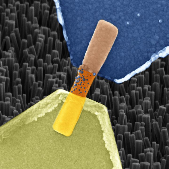
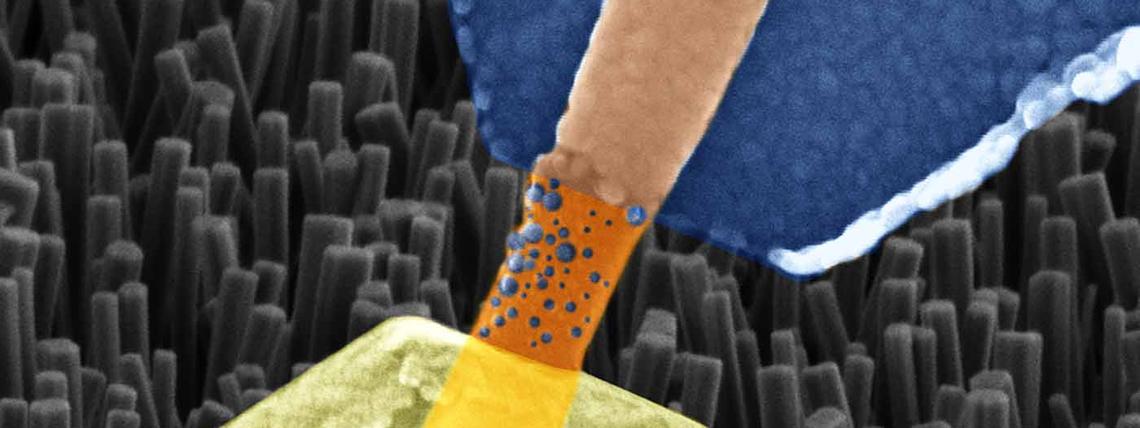
Neuromorphic architectures merge learning and memory functions within a single unit cell and in a neuron-like fashion. Research in the field has been mainly focused on the plasticity of artificial synapses. However, the intrinsic plasticity of the neuronal membrane is also important in the implementation of neuromorphic information processing. Here we report a neurotransistor made from a silicon nanowire transistor coated by an ion-doped sol–gel silicate film that can emulate the intrinsic plasticity of the neuronal membrane.

Caption: Neurotransistors: from silicon chips to neuromorphic architecture. Credit: TU Dresden / E. Baek Courtesy: Helmholtz-Zentrum Dresden-Rossendorf

A July 14, 2020 news item on Nanowerk announced the research (Note: A link has been removed),

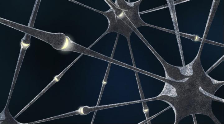
Especially activities in the field of artificial intelligence, like teaching robots to walk or precise automatic image recognition, demand ever more powerful, yet at the same time more economical computer chips. While the optimization of conventional microelectronics is slowly reaching its physical limits, nature offers us a blueprint how information can be processed and stored quickly and efficiently: our own brain.

For the very first time, scientists at TU Dresden and the Helmholtz-Zentrum Dresden-Rossendorf (HZDR) have now successfully imitated the functioning of brain neurons using semiconductor materials. They have published their research results in the journal Nature Electronics (“Intrinsic plasticity of silicon nanowire neurotransistors for dynamic memory and learning functions”).

A July 14, 2020 Helmholtz-Zentrum Dresden-Rossendorf press release (also on EurekAlert), which originated the news items delves further into the research,

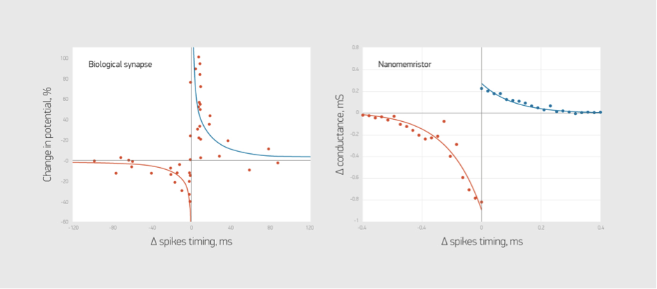
Today, enhancing the performance of microelectronics is usually achieved by reducing component size, especially of the individual transistors on the silicon computer chips. “But that can’t go on indefinitely – we need new approaches”, Larysa Baraban asserts. The physicist, who has been working at HZDR since the beginning of the year, is one of the three primary authors of the international study, which involved a total of six institutes. One approach is based on the brain, combining data processing with data storage in an artificial neuron.

“Our group has extensive experience with biological and chemical electronic sensors,” Baraban continues. “So, we simulated the properties of neurons using the principles of biosensors and modified a classical field-effect transistor to create an artificial neurotransistor.” The advantage of such an architecture lies in the simultaneous storage and processing of information in a single component. In conventional transistor technology, they are separated, which slows processing time and hence ultimately also limits performance.

Silicon wafer + polymer = chip capable of learning

Modeling computers on the human brain is no new idea. Scientists made attempts to hook up nerve cells to electronics in Petri dishes decades ago. “But a wet computer chip that has to be fed all the time is of no use to anybody,” says Gianaurelio Cuniberti from TU Dresden. The Professor for Materials Science and Nanotechnology is one of the three brains behind the neurotransistor alongside Ronald Tetzlaff, Professor of Fundamentals of Electrical Engineering in Dresden, and Leon Chua [emphasis mine] from the University of California at Berkeley, who had already postulated similar components in the early 1970s.

Now, Cuniberti, Baraban and their team have been able to implement it: “We apply a viscous substance – called solgel – to a conventional silicon wafer with circuits. This polymer hardens and becomes a porous ceramic,” the materials science professor explains. “Ions move between the holes. They are heavier than electrons and slower to return to their position after excitation. This delay, called hysteresis, is what causes the storage effect.” As Cuniberti explains, this is a decisive factor in the functioning of the transistor. “The more an individual transistor is excited, the sooner it will open and let the current flow. This strengthens the connection. The system is learning.”

Cuniberti and his team are not focused on conventional issues, though. “Computers based on our chip would be less precise and tend to estimate mathematical computations rather than calculating them down to the last decimal,” the scientist explains. “But they would be more intelligent. For example, a robot with such processors would learn to walk or grasp; it would possess an optical system and learn to recognize connections. And all this without having to develop any software.” But these are not the only advantages of neuromorphic computers. Thanks to their plasticity, which is similar to that of the human brain, they can adapt to changing tasks during operation and, thus, solve problems for which they were not originally programmed.

I highlighted Dr. Leon Chua’s name as he was one of the first to conceptualize the notion of a memristor (memory resistor), which is what the press release seems to be referencing with the mention of artificial synapses. Dr. Chua very kindly answered a few questions for me about his work which I published in an April 13, 2010 posting (scroll down about 40% of the way).

Using light to manipulate neurons

There are three (or more?) possible applications including neuromorphic computing for this new optoelectronic technology which is based on black phophorus. A July 16, 2019 news item on Nanowerk announces the research,

Researchers from RMIT University [Australia] drew inspiration from an emerging tool in biotechnology – optogenetics – to develop a device that replicates the way the brain stores and loses information.

Optogenetics allows scientists to delve into the body’s electrical system with incredible precision, using light to manipulate neurons so that they can be turned on or off.

The new chip is based on an ultra-thin material that changes electrical resistance in response to different wavelengths of light, enabling it to mimic the way that neurons work to store and delete information in the brain.

Caption: The new chip is based on an ultra-thin material that changes electrical resistance in response to different wavelengths of light. Credit: RMIT University

A July 17, 2019 RMIT University press release (also on EurekAlert but published on July 16, 2019), which originated the news item, expands on the theme,

Research team leader Dr Sumeet Walia said the technology moves us closer towards artificial intelligence (AI) that can harness the brain’s full sophisticated functionality.

“Our optogenetically-inspired chip imitates the fundamental biology of nature’s best computer – the human brain,” Walia said.

“Being able to store, delete and process information is critical for computing, and the brain does this extremely efficiently.

“We’re able to simulate the brain’s neural approach simply by shining different colours onto our chip.

“This technology takes us further on the path towards fast, efficient and secure light-based computing.

“It also brings us an important step closer to the realisation of a bionic brain – a brain-on-a-chip that can learn from its environment just like humans do.”

Dr Taimur Ahmed, lead author of the study published in Advanced Functional Materials, said being able to replicate neural behavior on an artificial chip offered exciting avenues for research across sectors.

“This technology creates tremendous opportunities for researchers to better understand the brain and how it’s affected by disorders that disrupt neural connections, like Alzheimer’s disease and dementia,” Ahmed said.

The researchers, from the Functional Materials and Microsystems Research Group at RMIT, have also demonstrated the chip can perform logic operations – information processing – ticking another box for brain-like functionality.

Developed at RMIT’s MicroNano Research Facility, the technology is compatible with existing electronics and has also been demonstrated on a flexible platform, for integration into wearable electronics.

How the chip works:

Neural connections happen in the brain through electrical impulses. When tiny energy spikes reach a certain threshold of voltage, the neurons bind together – and you’ve started creating a memory.

On the chip, light is used to generate a photocurrent. Switching between colors causes the current to reverse direction from positive to negative.

This direction switch, or polarity shift, is equivalent to the binding and breaking of neural connections, a mechanism that enables neurons to connect (and induce learning) or inhibit (and induce forgetting).

This is akin to optogenetics, where light-induced modification of neurons causes them to either turn on or off, enabling or inhibiting connections to the next neuron in the chain.

To develop the technology, the researchers used a material called black phosphorus (BP) that can be inherently defective in nature.

This is usually a problem for optoelectronics, but with precision engineering the researchers were able to harness the defects to create new functionality.

“Defects are usually looked on as something to be avoided, but here we’re using them to create something novel and useful,” Ahmed said.

“It’s a creative approach to finding solutions for the technical challenges we face.”

Here’s a link and a citation for the paper,

Multifunctional Optoelectronics via Harnessing Defects in Layered Black Phosphorus by Taimur Ahmed, Sruthi Kuriakose, Sherif Abbas,, Michelle J. S. Spencer, Md. Ataur Rahman, Muhammad Tahir, Yuerui Lu, Prashant Sonar, Vipul Bansal, Madhu Bhaskaran, Sharath Sriram, Sumeet Walia. Advanced Functional Materials DOI: https://doi.org/10.1002/adfm.201901991 First published (online): 17 July 2019

This paper is behind a paywall.

Memristors with better mimicry of synapses

It seems to me it’s been quite a while since I’ve stumbled across a memristor story from the University of Micihigan but it was worth waiting for. (Much of the research around memristors has to do with their potential application in neuromorphic (brainlike) computers.) From a December 17, 2018 news item on ScienceDaily,

A new electronic device developed at the University of Michigan can directly model the behaviors of a synapse, which is a connection between two neurons.

For the first time, the way that neurons share or compete for resources can be explored in hardware without the need for complicated circuits.

“Neuroscientists have argued that competition and cooperation behaviors among synapses are very important. Our new memristive devices allow us to implement a faithful model of these behaviors in a solid-state system,” said Wei Lu, U-M professor of electrical and computer engineering and senior author of the study in Nature Materials.

A December 17, 2018 University of Michigan news release (also on EurekAlert), which originated the news item, provides an explanation of memristors and their ‘similarity’ to synapses while providing more details about this latest research,

Memristors are electrical resistors with memory–advanced electronic devices that regulate current based on the history of the voltages applied to them. They can store and process data simultaneously, which makes them a lot more efficient than traditional systems. They could enable new platforms that process a vast number of signals in parallel and are capable of advanced machine learning.

The memristor is a good model for a synapse. It mimics the way that the connections between neurons strengthen or weaken when signals pass through them. But the changes in conductance typically come from changes in the shape of the channels of conductive material within the memristor. These channels–and the memristor’s ability to conduct electricity–could not be precisely controlled in previous devices.

Now, the U-M team has made a memristor in which they have better command of the conducting pathways.They developed a new material out of the semiconductor molybdenum disulfide–a “two-dimensional” material that can be peeled into layers just a few atoms thick. Lu’s team injected lithium ions into the gaps between molybdenum disulfide layers.
They found that if there are enough lithium ions present, the molybdenum sulfide transforms its lattice structure, enabling electrons to run through the film easily as if it were a metal. But in areas with too few lithium ions, the molybdenum sulfide restores its original lattice structure and becomes a semiconductor, and electrical signals have a hard time getting through.

The lithium ions are easy to rearrange within the layer by sliding them with an electric field. This changes the size of the regions that conduct electricity little by little and thereby controls the device’s conductance.

“Because we change the ‘bulk’ properties of the film, the conductance change is much more gradual and much more controllable,” Lu said.

In addition to making the devices behave better, the layered structure enabled Lu’s team to link multiple memristors together through shared lithium ions–creating a kind of connection that is also found in brains. A single neuron’s dendrite, or its signal-receiving end, may have several synapses connecting it to the signaling arms of other neurons. Lu compares the availability of lithium ions to that of a protein that enables synapses to grow.

If the growth of one synapse releases these proteins, called plasticity-related proteins, other synapses nearby can also grow–this is cooperation. Neuroscientists have argued that cooperation between synapses helps to rapidly form vivid memories that last for decades and create associative memories, like a scent that reminds you of your grandmother’s house, for example. If the protein is scarce, one synapse will grow at the expense of the other–and this competition pares down our brains’ connections and keeps them from exploding with signals.
Lu’s team was able to show these phenomena directly using their memristor devices. In the competition scenario, lithium ions were drained away from one side of the device. The side with the lithium ions increased its conductance, emulating the growth, and the conductance of the device with little lithium was stunted.

In a cooperation scenario, they made a memristor network with four devices that can exchange lithium ions, and then siphoned some lithium ions from one device out to the others. In this case, not only could the lithium donor increase its conductance–the other three devices could too, although their signals weren’t as strong.

Lu’s team is currently building networks of memristors like these to explore their potential for neuromorphic computing, which mimics the circuitry of the brain.

Here’s a link to and a citation for the paper,

Ionic modulation and ionic coupling effects in MoS2 devices for neuromorphic computing by Xiaojian Zhu, Da Li, Xiaogan Liang, & Wei D. Lu. Nature Materials (2018) DOI: https://doi.org/10.1038/s41563-018-0248-5 Published 17 December 2018

This paper is behind a paywall.

The researchers have made images illustrating their work available,

A schematic of the molybdenum disulfide layers with lithium ions between them. On the right, the simplified inset shows how the molybdenum disulfide changes its atom arrangements in the presence and absence of the lithium atoms, between a metal (1T’ phase) and semiconductor (2H phase), respectively. Image credit: Xiaojian Zhu, Nanoelectronics Group, University of Michigan.

A diagram of a synapse receiving a signal from one of the connecting neurons. This signal activates the generation of plasticity-related proteins (PRPs), which help a synapse to grow. They can migrate to other synapses, which enables multiple synapses to grow at once. The new device is the first to mimic this process directly, without the need for software or complicated circuits. Image credit: Xiaojian Zhu, Nanoelectronics Group, University of Michigan.
An electron microscope image showing the rectangular gold (Au) electrodes representing signalling neurons and the rounded electrode representing the receiving neuron. The material of molybdenum disulfide layered with lithium connects the electrodes, enabling the simulation of cooperative growth among synapses. Image credit: Xiaojian Zhu, Nanoelectronics Group, University of Michigan.

That’s all folks.

An artificial synapse tuned by light, a ferromagnetic memristor, and a transparent, flexible artificial synapse

Down the memristor rabbit hole one more time.* I started out with news about two new papers and inadvertently found two more. In a bid to keep this posting to a manageable size, I’m stopping at four.

UK

In a June 19, 2019 Nanowerk Spotlight article, Dr. Neil Kemp discusses memristors and some of his latest work (Note: A link has been removed),

Memristor (or memory resistors) devices are non-volatile electronic memory devices that were first theorized by Leon Chua in the 1970’s. However, it was some thirty years later that the first practical device was fabricated. This was in 2008 when a group led by Stanley Williams at HP Research Labs realized that switching of the resistance between a conducting and less conducting state in metal-oxide thin-film devices was showing Leon Chua’s memristor behaviour.

The high interest in memristor devices also stems from the fact that these devices emulate the memory and learning properties of biological synapses. i.e. the electrical resistance value of the device is dependent on the history of the current flowing through it.

There is a huge effort underway to use memristor devices in neuromorphic computing applications and it is now reasonable to imagine the development of a new generation of artificial intelligent devices with very low power consumption (non-volatile), ultra-fast performance and high-density integration.

These discoveries come at an important juncture in microelectronics, since there is increasing disparity between computational needs of Big Data, Artificial Intelligence (A.I.) and the Internet of Things (IoT), and the capabilities of existing computers. The increases in speed, efficiency and performance of computer technology cannot continue in the same manner as it has done since the 1960s.

To date, most memristor research has focussed on the electronic switching properties of the device. However, for many applications it is useful to have an additional handle (or degree of freedom) on the device to control its resistive state. For example memory and processing in the brain also involves numerous chemical and bio-chemical reactions that control the brain structure and its evolution through development.

To emulate this in a simple solid-state system composed of just switches alone is not possible. In our research, we are interested in using light to mediate this essential control.

We have demonstrated that light can be used to make short and long-term memory and we have shown how light can modulate a special type of learning, called spike timing dependent plasticity (STDP). STDP involves two neuronal spikes incident across a synapse at the same time. Depending on the relative timing of the spikes and their overlap across the synaptic cleft, the connection strength is other strengthened or weakened.

In our earlier work, we were only able to achieve to small switching effects in memristors using light. In our latest work (Advanced Electronic Materials, “Percolation Threshold Enables Optical Resistive-Memory Switching and Light-Tuneable Synaptic Learning in Segregated Nanocomposites”), we take advantage of a percolating-like nanoparticle morphology to vastly increase the magnitude of the switching between electronic resistance states when light is incident on the device.

We have used an inhomogeneous percolating network consisting of metallic nanoparticles distributed in filamentary-like conduction paths. Electronic conduction and the resistance of the device is very sensitive to any disruption of the conduction path(s).

By embedding the nanoparticles in a polymer that can expand or contract with light the conduction pathways are broken or re-connected causing very large changes in the electrical resistance and memristance of the device.

Our devices could lead to the development of new memristor-based artificial intelligence systems that are adaptive and reconfigurable using a combination of optical and electronic signalling. Furthermore, they have the potential for the development of very fast optical cameras for artificial intelligence recognition systems.

Our work provides a nice proof-of-concept but the materials used means the optical switching is slow. The materials are also not well suited to industry fabrication. In our on-going work we are addressing these switching speed issues whilst also focussing on industry compatible materials.

Currently we are working on a new type of optical memristor device that should give us orders of magnitude improvement in the optical switching speeds whilst also retaining a large difference between the resistance on and off states. We hope to be able to achieve nanosecond switching speeds. The materials used are also compatible with industry standard methods of fabrication.

The new devices should also have applications in optical communications, interfacing and photonic computing. We are currently looking for commercial investors to help fund the research on these devices so that we can bring the device specifications to a level of commercial interest.

If you’re interested in memristors, Kemp’s article is well written and quite informative for nonexperts, assuming of course you can tolerate not understanding everything perfectly.

Here are links and citations for two papers. The first is the latest referred to in the article, a May 2019 paper and the second is a paper appearing in July 2019.

Percolation Threshold Enables Optical Resistive‐Memory Switching and Light‐Tuneable Synaptic Learning in Segregated Nanocomposites by Ayoub H. Jaafar, Mary O’Neill, Stephen M. Kelly, Emanuele Verrelli, Neil T. Kemp. Advanced Electronic Materials DOI: https://doi.org/10.1002/aelm.201900197 First published: 28 May 2019

Wavelength dependent light tunable resistive switching graphene oxide nonvolatile memory devices by Ayoub H.Jaafar, N.T.Kemp. DOI: https://doi.org/10.1016/j.carbon.2019.07.007 Carbon Available online 3 July 2019

The first paper (May 2019) is definitely behind a paywall and the second paper (July 2019) appears to be behind a paywall.

Dr. Kemp’s work has been featured here previously in a January 3, 2018 posting in the subsection titled, Shining a light on the memristor.

China

This work from China was announced in a June 20, 2019 news item on Nanowerk,

Memristors, demonstrated by solid-state devices with continuously tunable resistance, have emerged as a new paradigm for self-adaptive networks that require synapse-like functions. Spin-based memristors offer advantages over other types of memristors because of their significant endurance and high energy effciency.

However, it remains a challenge to build dense and functional spintronic memristors with structures and materials that are compatible with existing ferromagnetic devices. Ta/CoFeB/MgO heterostructures are commonly used in interfacial PMA-based [perpendicular magnetic anisotropy] magnetic tunnel junctions, which exhibit large tunnel magnetoresistance and are implemented in commercial MRAM [magnetic random access memory] products.

“To achieve the memristive function, DW is driven back and forth in a continuous manner in the CoFeB layer by applying in-plane positive or negative current pulses along the Ta layer, utilizing SOT that the current exerts on the CoFeB magnetization,” said Shuai Zhang, a coauthor in the paper. “Slowly propagating domain wall generates a creep in the detection area of the device, which yields a broad range of intermediate resistive states in the AHE [anomalous Hall effect] measurements. Consequently, AHE resistance is modulated in an analog manner, being controlled by the pulsed current characteristics including amplitude, duration, and repetition number.”

“For a follow-up study, we are working on more neuromorphic operations, such as spike-timing-dependent plasticity and paired pulsed facilitation,” concludes You. …

Here’s are links to and citations for the paper (Note: It’s a little confusing but I believe that one of the links will take you to the online version, as for the ‘open access’ link, keep reading),

A Spin–Orbit‐Torque Memristive Device by Shuai Zhang, Shijiang Luo, Nuo Xu, Qiming Zou, Min Song, Jijun Yun, Qiang Luo, Zhe Guo, Ruofan Li, Weicheng Tian, Xin Li, Hengan Zhou, Huiming Chen, Yue Zhang, Xiaofei Yang, Wanjun Jiang, Ka Shen, Jeongmin Hong, Zhe Yuan, Li Xi, Ke Xia, Sayeef Salahuddin, Bernard Dieny, Long You. Advanced Electronic Materials Volume 5, Issue 4 April 2019 (print version) 1800782 DOI: https://doi.org/10.1002/aelm.201800782 First published [online]: 30 January 2019 Note: there is another DOI, https://doi.org/10.1002/aelm.201970022 where you can have open access to Memristors: A Spin–Orbit‐Torque Memristive Device (Adv. Electron. Mater. 4/2019)

The paper published online in January 2019 is behind a paywall and the paper (almost the same title) published in April 2019 has a new DOI and is open access. Final note: I tried accessing the ‘free’ paper and opened up a free file for the artwork featuring the work from China on the back cover of the April 2019 of Advanced Electronic Materials.

Korea

Usually when I see the words transparency and flexibility, I expect to see graphene is one of the materials. That’s not the case for this paper (link to and citation for),

Transparent and flexible photonic artificial synapse with piezo-phototronic modulator: Versatile memory capability and higher order learning algorithm by Mohit Kumar, Joondong Kim, Ching-Ping Wong. Nano Energy Volume 63, September 2019, 103843 DOI: https://doi.org/10.1016/j.nanoen.2019.06.039 Available online 22 June 2019

Here’s the abstract for the paper where you’ll see that the material is made up of zinc oxide silver nanowires,

An artificial photonic synapse having tunable manifold synaptic response can be an essential step forward for the advancement of novel neuromorphic computing. In this work, we reported the development of highly transparent and flexible two-terminal ZnO/Ag-nanowires/PET photonic artificial synapse [emphasis mine]. The device shows purely photo-triggered all essential synaptic functions such as transition from short-to long-term plasticity, paired-pulse facilitation, and spike-timing-dependent plasticity, including in the versatile memory capability. Importantly, strain-induced piezo-phototronic effect within ZnO provides an additional degree of regulation to modulate all of the synaptic functions in multi-levels. The observed effect is quantitatively explained as a dynamic of photo-induced electron-hole trapping/detraining via the defect states such as oxygen vacancies. We revealed that the synaptic functions can be consolidated and converted by applied strain, which is not previously applied any of the reported synaptic devices. This study will open a new avenue to the scientific community to control and design highly transparent wearable neuromorphic computing.

This paper is behind a paywall.

Artificial synapse courtesy of nanowires

It looks like a popsicle to me,

Caption: Image captured by an electron microscope of a single nanowire memristor (highlighted in colour to distinguish it from other nanowires in the background image). Blue: silver electrode, orange: nanowire, yellow: platinum electrode. Blue bubbles are dispersed over the nanowire. They are made up of silver ions and form a bridge between the electrodes which increases the resistance. Credit: Forschungszentrum Jülich

Not a popsicle but a representation of a device (memristor) scientists claim mimics a biological nerve cell according to a December 5, 2018 news item on ScienceDaily,

Scientists from Jülich [Germany] together with colleagues from Aachen [Germany] and Turin [Italy] have produced a memristive element made from nanowires that functions in much the same way as a biological nerve cell. The component is able to both save and process information, as well as receive numerous signals in parallel. The resistive switching cell made from oxide crystal nanowires is thus proving to be the ideal candidate for use in building bioinspired “neuromorphic” processors, able to take over the diverse functions of biological synapses and neurons.

A Dec. 5, 2018 Forschungszentrum Jülich press release (also on EurekAlert), which originated the news item, provides more details,

Computers have learned a lot in recent years. Thanks to rapid progress in artificial intelligence they are now able to drive cars, translate texts, defeat world champions at chess, and much more besides. In doing so, one of the greatest challenges lies in the attempt to artificially reproduce the signal processing in the human brain. In neural networks, data are stored and processed to a high degree in parallel. Traditional computers on the other hand rapidly work through tasks in succession and clearly distinguish between the storing and processing of information. As a rule, neural networks can only be simulated in a very cumbersome and inefficient way using conventional hardware.

Systems with neuromorphic chips that imitate the way the human brain works offer significant advantages. Experts in the field describe this type of bioinspired computer as being able to work in a decentralised way, having at its disposal a multitude of processors, which, like neurons in the brain, are connected to each other by networks. If a processor breaks down, another can take over its function. What is more, just like in the brain, where practice leads to improved signal transfer, a bioinspired processor should have the capacity to learn.

“With today’s semiconductor technology, these functions are to some extent already achievable. These systems are however suitable for particular applications and require a lot of space and energy,” says Dr. Ilia Valov from Forschungszentrum Jülich. “Our nanowire devices made from zinc oxide crystals can inherently process and even store information, as well as being extremely small and energy efficient,” explains the researcher from Jülich’s Peter Grünberg Institute.

For years memristive cells have been ascribed the best chances of being capable of taking over the function of neurons and synapses in bioinspired computers. They alter their electrical resistance depending on the intensity and direction of the electric current flowing through them. In contrast to conventional transistors, their last resistance value remains intact even when the electric current is switched off. Memristors are thus fundamentally capable of learning.

In order to create these properties, scientists at Forschungszentrum Jülich and RWTH Aachen University used a single zinc oxide nanowire, produced by their colleagues from the polytechnic university in Turin. Measuring approximately one ten-thousandth of a millimeter in size, this type of nanowire is over a thousand times thinner than a human hair. The resulting memristive component not only takes up a tiny amount of space, but also is able to switch much faster than flash memory.

Nanowires offer promising novel physical properties compared to other solids and are used among other things in the development of new types of solar cells, sensors, batteries and computer chips. Their manufacture is comparatively simple. Nanowires result from the evaporation deposition of specified materials onto a suitable substrate, where they practically grow of their own accord.

In order to create a functioning cell, both ends of the nanowire must be attached to suitable metals, in this case platinum and silver. The metals function as electrodes, and in addition, release ions triggered by an appropriate electric current. The metal ions are able to spread over the surface of the wire and build a bridge to alter its conductivity.

Components made from single nanowires are, however, still too isolated to be of practical use in chips. Consequently, the next step being planned by the Jülich and Turin researchers is to produce and study a memristive element, composed of a larger, relatively easy to generate group of several hundred nanowires offering more exciting functionalities.

The Italians have also written about the work in a December 4, 2018 news item for the Polytecnico di Torino’s inhouse magazine, PoliFlash’. I like the image they’ve used better as it offers a bit more detail and looks less like a popsicle. First, the image,

Courtesy: Polytecnico di Torino

Now, the news item, which includes some historical information about the memristor (Note: There is some repetition and links have been removed),

Emulating and understanding the human brain is one of the most important challenges for modern technology: on the one hand, the ability to artificially reproduce the processing of brain signals is one of the cornerstones for the development of artificial intelligence, while on the other the understanding of the cognitive processes at the base of the human mind is still far away.

And the research published in the prestigious journal Nature Communications by Gianluca Milano and Carlo Ricciardi, PhD student and professor, respectively, of the Applied Science and Technology Department of the Politecnico di Torino, represents a step forward in these directions. In fact, the study entitled “Self-limited single nanowire systems combining all-in-one memristive and neuromorphic functionalities” shows how it is possible to artificially emulate the activity of synapses, i.e. the connections between neurons that regulate the learning processes in our brain, in a single “nanowire” with a diameter thousands of times smaller than that of a hair.

It is a crystalline nanowire that takes the “memristor”, the electronic device able to artificially reproduce the functions of biological synapses, to a more performing level. Thanks to the use of nanotechnologies, which allow the manipulation of matter at the atomic level, it was for the first time possible to combine into one single device the synaptic functions that were individually emulated through specific devices. For this reason, the nanowire allows an extreme miniaturisation of the “memristor”, significantly reducing the complexity and energy consumption of the electronic circuits necessary for the implementation of learning algorithms.

Starting from the theorisation of the “memristor” in 1971 by Prof. Leon Chua – now visiting professor at the Politecnico di Torino, who was conferred an honorary degree by the University in 2015 – this new technology will not only allow smaller and more performing devices to be created for the implementation of increasingly “intelligent” computers, but is also a significant step forward for the emulation and understanding of the functioning of the brain.

“The nanowire memristor – said Carlo Ricciardirepresents a model system for the study of physical and electrochemical phenomena that govern biological synapses at the nanoscale. The work is the result of the collaboration between our research team and the RWTH University of Aachen in Germany, supported by INRiM, the National Institute of Metrological Research, and IIT, the Italian Institute of Technology.”

h.t for the Italian info. to Nanowerk’s Dec. 10, 2018 news item.

Here’s a link to and a citation for the paper,

Self-limited single nanowire systems combining all-in-one memristive and neuromorphic functionalities by Gianluca Milano, Michael Luebben, Zheng Ma, Rafal Dunin-Borkowski, Luca Boarino, Candido F. Pirri, Rainer Waser, Carlo Ricciardi, & Ilia Valov. Nature Communicationsvolume 9, Article number: 5151 (2018) DOI: https://doi.org/10.1038/s41467-018-07330-7 Published: 04 December 2018

This paper is open access.

Just use the search term “memristor” in the blog search engine if you’re curious about the multitudinous number of postings on the topic here.

Brainy and brainy: a novel synaptic architecture and a neuromorphic computing platform called SpiNNaker

I have two items about brainlike computing. The first item hearkens back to memristors, a topic I have been following since 2008. (If you’re curious about the various twists and turns just enter  the term ‘memristor’ in this blog’s search engine.) The latest on memristors is from a team than includes IBM (US), École Politechnique Fédérale de Lausanne (EPFL; Swizterland), and the New Jersey Institute of Technology (NJIT; US). The second bit comes from a Jülich Research Centre team in Germany and concerns an approach to brain-like computing that does not include memristors.

Multi-memristive synapses

In the inexorable march to make computers function more like human brains (neuromorphic engineering/computing), an international team has announced its latest results in a July 10, 2018 news item on Nanowerk,

Two New Jersey Institute of Technology (NJIT) researchers, working with collaborators from the IBM Research Zurich Laboratory and the École Polytechnique Fédérale de Lausanne, have demonstrated a novel synaptic architecture that could lead to a new class of information processing systems inspired by the brain.

The findings are an important step toward building more energy-efficient computing systems that also are capable of learning and adaptation in the real world. …

A July 10, 2018 NJIT news release (also on EurekAlert) by Tracey Regan, which originated by the news item, adds more details,

The researchers, Bipin Rajendran, an associate professor of electrical and computer engineering, and S. R. Nandakumar, a graduate student in electrical engineering, have been developing brain-inspired computing systems that could be used for a wide range of big data applications.

Over the past few years, deep learning algorithms have proven to be highly successful in solving complex cognitive tasks such as controlling self-driving cars and language understanding. At the heart of these algorithms are artificial neural networks – mathematical models of the neurons and synapses of the brain – that are fed huge amounts of data so that the synaptic strengths are autonomously adjusted to learn the intrinsic features and hidden correlations in these data streams.

However, the implementation of these brain-inspired algorithms on conventional computers is highly inefficient, consuming huge amounts of power and time. This has prompted engineers to search for new materials and devices to build special-purpose computers that can incorporate the algorithms. Nanoscale memristive devices, electrical components whose conductivity depends approximately on prior signaling activity, can be used to represent the synaptic strength between the neurons in artificial neural networks.

While memristive devices could potentially lead to faster and more power-efficient computing systems, they are also plagued by several reliability issues that are common to nanoscale devices. Their efficiency stems from their ability to be programmed in an analog manner to store multiple bits of information; however, their electrical conductivities vary in a non-deterministic and non-linear fashion.

In the experiment, the team showed how multiple nanoscale memristive devices exhibiting these characteristics could nonetheless be configured to efficiently implement artificial intelligence algorithms such as deep learning. Prototype chips from IBM containing more than one million nanoscale phase-change memristive devices were used to implement a neural network for the detection of hidden patterns and correlations in time-varying signals.

“In this work, we proposed and experimentally demonstrated a scheme to obtain high learning efficiencies with nanoscale memristive devices for implementing learning algorithms,” Nandakumar says. “The central idea in our demonstration was to use several memristive devices in parallel to represent the strength of a synapse of a neural network, but only chose one of them to be updated at each step based on the neuronal activity.”

Here’s a link to and a citation for the paper,

Neuromorphic computing with multi-memristive synapses by Irem Boybat, Manuel Le Gallo, S. R. Nandakumar, Timoleon Moraitis, Thomas Parnell, Tomas Tuma, Bipin Rajendran, Yusuf Leblebici, Abu Sebastian, & Evangelos Eleftheriou. Nature Communications volume 9, Article number: 2514 (2018) DOI: https://doi.org/10.1038/s41467-018-04933-y Published 28 June 2018

This is an open access paper.

Also they’ve got a couple of very nice introductory paragraphs which I’m including here, (from the June 28, 2018 paper in Nature Communications; Note: Links have been removed),

The human brain with less than 20 W of power consumption offers a processing capability that exceeds the petaflops mark, and thus outperforms state-of-the-art supercomputers by several orders of magnitude in terms of energy efficiency and volume. Building ultra-low-power cognitive computing systems inspired by the operating principles of the brain is a promising avenue towards achieving such efficiency. Recently, deep learning has revolutionized the field of machine learning by providing human-like performance in areas, such as computer vision, speech recognition, and complex strategic games1. However, current hardware implementations of deep neural networks are still far from competing with biological neural systems in terms of real-time information-processing capabilities with comparable energy consumption.

One of the reasons for this inefficiency is that most neural networks are implemented on computing systems based on the conventional von Neumann architecture with separate memory and processing units. There are a few attempts to build custom neuromorphic hardware that is optimized to implement neural algorithms2,3,4,5. However, as these custom systems are typically based on conventional silicon complementary metal oxide semiconductor (CMOS) circuitry, the area efficiency of such hardware implementations will remain relatively low, especially if in situ learning and non-volatile synaptic behavior have to be incorporated. Recently, a new class of nanoscale devices has shown promise for realizing the synaptic dynamics in a compact and power-efficient manner. These memristive devices store information in their resistance/conductance states and exhibit conductivity modulation based on the programming history6,7,8,9. The central idea in building cognitive hardware based on memristive devices is to store the synaptic weights as their conductance states and to perform the associated computational tasks in place.

The two essential synaptic attributes that need to be emulated by memristive devices are the synaptic efficacy and plasticity. …

It gets more complicated from there.

Now onto the next bit.

SpiNNaker

At a guess, those capitalized N’s are meant to indicate ‘neural networks’. As best I can determine, SpiNNaker is not based on the memristor. Moving on, a July 11, 2018 news item on phys.org announces work from a team examining how neuromorphic hardware and neuromorphic software work together,

A computer built to mimic the brain’s neural networks produces similar results to that of the best brain-simulation supercomputer software currently used for neural-signaling research, finds a new study published in the open-access journal Frontiers in Neuroscience. Tested for accuracy, speed and energy efficiency, this custom-built computer named SpiNNaker, has the potential to overcome the speed and power consumption problems of conventional supercomputers. The aim is to advance our knowledge of neural processing in the brain, to include learning and disorders such as epilepsy and Alzheimer’s disease.

A July 11, 2018 Frontiers Publishing news release on EurekAlert, which originated the news item, expands on the latest work,

“SpiNNaker can support detailed biological models of the cortex–the outer layer of the brain that receives and processes information from the senses–delivering results very similar to those from an equivalent supercomputer software simulation,” says Dr. Sacha van Albada, lead author of this study and leader of the Theoretical Neuroanatomy group at the Jülich Research Centre, Germany. “The ability to run large-scale detailed neural networks quickly and at low power consumption will advance robotics research and facilitate studies on learning and brain disorders.”

The human brain is extremely complex, comprising 100 billion interconnected brain cells. We understand how individual neurons and their components behave and communicate with each other and on the larger scale, which areas of the brain are used for sensory perception, action and cognition. However, we know less about the translation of neural activity into behavior, such as turning thought into muscle movement.

Supercomputer software has helped by simulating the exchange of signals between neurons, but even the best software run on the fastest supercomputers to date can only simulate 1% of the human brain.

“It is presently unclear which computer architecture is best suited to study whole-brain networks efficiently. The European Human Brain Project and Jülich Research Centre have performed extensive research to identify the best strategy for this highly complex problem. Today’s supercomputers require several minutes to simulate one second of real time, so studies on processes like learning, which take hours and days in real time are currently out of reach.” explains Professor Markus Diesmann, co-author, head of the Computational and Systems Neuroscience department at the Jülich Research Centre.

He continues, “There is a huge gap between the energy consumption of the brain and today’s supercomputers. Neuromorphic (brain-inspired) computing allows us to investigate how close we can get to the energy efficiency of the brain using electronics.”

Developed over the past 15 years and based on the structure and function of the human brain, SpiNNaker — part of the Neuromorphic Computing Platform of the Human Brain Project — is a custom-built computer composed of half a million of simple computing elements controlled by its own software. The researchers compared the accuracy, speed and energy efficiency of SpiNNaker with that of NEST–a specialist supercomputer software currently in use for brain neuron-signaling research.

“The simulations run on NEST and SpiNNaker showed very similar results,” reports Steve Furber, co-author and Professor of Computer Engineering at the University of Manchester, UK. “This is the first time such a detailed simulation of the cortex has been run on SpiNNaker, or on any neuromorphic platform. SpiNNaker comprises 600 circuit boards incorporating over 500,000 small processors in total. The simulation described in this study used just six boards–1% of the total capability of the machine. The findings from our research will improve the software to reduce this to a single board.”

Van Albada shares her future aspirations for SpiNNaker, “We hope for increasingly large real-time simulations with these neuromorphic computing systems. In the Human Brain Project, we already work with neuroroboticists who hope to use them for robotic control.”

Before getting to the link and citation for the paper, here’s a description of SpiNNaker’s hardware from the ‘Spiking neural netowrk’ Wikipedia entry, Note: Links have been removed,

Neurogrid, built at Stanford University, is a board that can simulate spiking neural networks directly in hardware. SpiNNaker (Spiking Neural Network Architecture) [emphasis mine], designed at the University of Manchester, uses ARM processors as the building blocks of a massively parallel computing platform based on a six-layer thalamocortical model.[5]

Now for the link and citation,

Performance Comparison of the Digital Neuromorphic Hardware SpiNNaker and the Neural Network Simulation Software NEST for a Full-Scale Cortical Microcircuit Model by
Sacha J. van Albada, Andrew G. Rowley, Johanna Senk, Michael Hopkins, Maximilian Schmidt, Alan B. Stokes, David R. Lester, Markus Diesmann, and Steve B. Furber. Neurosci. 12:291. doi: 10.3389/fnins.2018.00291 Published: 23 May 2018

As noted earlier, this is an open access paper.

Announcing the ‘memtransistor’

Yet another advance toward ‘brainlike’ computing (how many times have I written this or a variation thereof in the last 10 years? See: Dexter Johnson’s take on the situation at the end of this post): Northwestern University announced their latest memristor research in a February 21, 2018 news item on Nanowerk,

Computer algorithms might be performing brain-like functions, such as facial recognition and language translation, but the computers themselves have yet to operate like brains.

“Computers have separate processing and memory storage units, whereas the brain uses neurons to perform both functions,” said Northwestern University’s Mark C. Hersam. “Neural networks can achieve complicated computation with significantly lower energy consumption compared to a digital computer.”

A February 21, 2018 Northwestern University news release (also on EurekAlert), which originated the news item, provides more information about the latest work from this team,

In recent years, researchers have searched for ways to make computers more neuromorphic, or brain-like, in order to perform increasingly complicated tasks with high efficiency. Now Hersam, a Walter P. Murphy Professor of Materials Science and Engineering in Northwestern’s McCormick School of Engineering, and his team are bringing the world closer to realizing this goal.

The research team has developed a novel device called a “memtransistor,” which operates much like a neuron by performing both memory and information processing. With combined characteristics of a memristor and transistor, the memtransistor also encompasses multiple terminals that operate more similarly to a neural network.

Supported by the National Institute of Standards and Technology and the National Science Foundation, the research was published online today, February 22 [2018], in Nature. Vinod K. Sangwan and Hong-Sub Lee, postdoctoral fellows advised by Hersam, served as the paper’s co-first authors.

The memtransistor builds upon work published in 2015, in which Hersam, Sangwan, and their collaborators used single-layer molybdenum disulfide (MoS2) to create a three-terminal, gate-tunable memristor for fast, reliable digital memory storage. Memristor, which is short for “memory resistors,” are resistors in a current that “remember” the voltage previously applied to them. Typical memristors are two-terminal electronic devices, which can only control one voltage channel. By transforming it into a three-terminal device, Hersam paved the way for memristors to be used in more complex electronic circuits and systems, such as neuromorphic computing.

To develop the memtransistor, Hersam’s team again used atomically thin MoS2 with well-defined grain boundaries, which influence the flow of current. Similar to the way fibers are arranged in wood, atoms are arranged into ordered domains – called “grains” – within a material. When a large voltage is applied, the grain boundaries facilitate atomic motion, causing a change in resistance.

“Because molybdenum disulfide is atomically thin, it is easily influenced by applied electric fields,” Hersam explained. “This property allows us to make a transistor. The memristor characteristics come from the fact that the defects in the material are relatively mobile, especially in the presence of grain boundaries.”

But unlike his previous memristor, which used individual, small flakes of MoS2, Hersam’s memtransistor makes use of a continuous film of polycrystalline MoS2 that comprises a large number of smaller flakes. This enabled the research team to scale up the device from one flake to many devices across an entire wafer.

“When length of the device is larger than the individual grain size, you are guaranteed to have grain boundaries in every device across the wafer,” Hersam said. “Thus, we see reproducible, gate-tunable memristive responses across large arrays of devices.”

After fabricating memtransistors uniformly across an entire wafer, Hersam’s team added additional electrical contacts. Typical transistors and Hersam’s previously developed memristor each have three terminals. In their new paper, however, the team realized a seven-terminal device, in which one terminal controls the current among the other six terminals.

“This is even more similar to neurons in the brain,” Hersam said, “because in the brain, we don’t usually have one neuron connected to only one other neuron. Instead, one neuron is connected to multiple other neurons to form a network. Our device structure allows multiple contacts, which is similar to the multiple synapses in neurons.”

Next, Hersam and his team are working to make the memtransistor faster and smaller. Hersam also plans to continue scaling up the device for manufacturing purposes.

“We believe that the memtransistor can be a foundational circuit element for new forms of neuromorphic computing,” he said. “However, making dozens of devices, as we have done in our paper, is different than making a billion, which is done with conventional transistor technology today. Thus far, we do not see any fundamental barriers that will prevent further scale up of our approach.”

The researchers have made this illustration available,

Caption: This is the memtransistor symbol overlaid on an artistic rendering of a hypothetical circuit layout in the shape of a brain. Credit; Hersam Research Group

Here’s a link to and a citation for the paper,

Multi-terminal memtransistors from polycrystalline monolayer molybdenum disulfide by Vinod K. Sangwan, Hong-Sub Lee, Hadallia Bergeron, Itamar Balla, Megan E. Beck, Kan-Sheng Chen, & Mark C. Hersam. Nature volume 554, pages 500–504 (22 February 2018 doi:10.1038/nature25747 Published online: 21 February 2018

This paper is behind a paywall.

The team’s earlier work referenced in the news release was featured here in an April 10, 2015 posting.

Dexter Johnson

From a Feb. 23, 2018 posting by Dexter Johnson on the Nanoclast blog (on the IEEE [Institute of Electrical and Electronics Engineers] website),

While this all seems promising, one of the big shortcomings in neuromorphic computing has been that it doesn’t mimic the brain in a very important way. In the brain, for every neuron there are a thousand synapses—the electrical signal sent between the neurons of the brain. This poses a problem because a transistor only has a single terminal, hardly an accommodating architecture for multiplying signals.

Now researchers at Northwestern University, led by Mark Hersam, have developed a new device that combines memristors—two-terminal non-volatile memory devices based on resistance switching—with transistors to create what Hersam and his colleagues have dubbed a “memtransistor” that performs both memory storage and information processing.

This most recent research builds on work that Hersam and his team conducted back in 2015 in which the researchers developed a three-terminal, gate-tunable memristor that operated like a kind of synapse.

While this work was recognized as mimicking the low-power computing of the human brain, critics didn’t really believe that it was acting like a neuron since it could only transmit a signal from one artificial neuron to another. This was far short of a human brain that is capable of making tens of thousands of such connections.

“Traditional memristors are two-terminal devices, whereas our memtransistors combine the non-volatility of a two-terminal memristor with the gate-tunability of a three-terminal transistor,” said Hersam to IEEE Spectrum. “Our device design accommodates additional terminals, which mimic the multiple synapses in neurons.”

Hersam believes that these unique attributes of these multi-terminal memtransistors are likely to present a range of new opportunities for non-volatile memory and neuromorphic computing.

If you have the time and the interest, Dexter’s post provides more context,

Does understanding your pet mean understanding artificial intelligence better?

Heather Roff’s take on artificial intelligence features an approach I haven’t seen before. From her March 30, 2017 essay for The Conversation (h/t March 31, 2017 news item on phys.org),

It turns out, though, that we already have a concept we can use when we think about AI: It’s how we think about animals. As a former animal trainer (albeit briefly) who now studies how people use AI, I know that animals and animal training can teach us quite a lot about how we ought to think about, approach and interact with artificial intelligence, both now and in the future.

Using animal analogies can help regular people understand many of the complex aspects of artificial intelligence. It can also help us think about how best to teach these systems new skills and, perhaps most importantly, how we can properly conceive of their limitations, even as we celebrate AI’s new possibilities.
Looking at constraints

As AI expert Maggie Boden explains, “Artificial intelligence seeks to make computers do the sorts of things that minds can do.” AI researchers are working on teaching computers to reason, perceive, plan, move and make associations. AI can see patterns in large data sets, predict the likelihood of an event occurring, plan a route, manage a person’s meeting schedule and even play war-game scenarios.

Many of these capabilities are, in themselves, unsurprising: Of course a robot can roll around a space and not collide with anything. But somehow AI seems more magical when the computer starts to put these skills together to accomplish tasks.

Thinking of AI as a trainable animal isn’t just useful for explaining it to the general public. It is also helpful for the researchers and engineers building the technology. If an AI scholar is trying to teach a system a new skill, thinking of the process from the perspective of an animal trainer could help identify potential problems or complications.

For instance, if I try to train my dog to sit, and every time I say “sit” the buzzer to the oven goes off, then my dog will begin to associate sitting not only with my command, but also with the sound of the oven’s buzzer. In essence, the buzzer becomes another signal telling the dog to sit, which is called an “accidental reinforcement.” If we look for accidental reinforcements or signals in AI systems that are not working properly, then we’ll know better not only what’s going wrong, but also what specific retraining will be most effective.

This requires us to understand what messages we are giving during AI training, as well as what the AI might be observing in the surrounding environment. The oven buzzer is a simple example; in the real world it will be far more complicated.

Before we welcome our AI overlords and hand over our lives and jobs to robots, we ought to pause and think about the kind of intelligences we are creating. …

Source: pixabay.com

It’s just last year (2016) that an AI system beat a human Go master player. Here’s how a March 17, 2016 article by John Russell for TechCrunch described the feat (Note: Links have been removed),

Much was written of an historic moment for artificial intelligence last week when a Google-developed AI beat one of the planet’s most sophisticated players of Go, an East Asia strategy game renowned for its deep thinking and strategy.

Go is viewed as one of the ultimate tests for an AI given the sheer possibilities on hand. “There are 1,000,000,000,000,000,000,000,000,000,000,000,000,000,000,000,000,000,000,000,000,000,000,000,000,000,000,000,000,000,000,000,000,000,000,000,000,000,000,000,000,000,000,000,000,000,000,000,000,000,000,000,000,000,000,000,000,000 possible positions [in the game] — that’s more than the number of atoms in the universe, and more than a googol times larger than chess,” Google said earlier this year.

If you missed the series — which AlphaGo, the AI, won 4-1 — or were unsure of exactly why it was so significant, Google summed the general importance up in a post this week.

Far from just being a game, Demis Hassabis, CEO and Co-Founder of DeepMind — the Google-owned company behind AlphaGo — said the AI’s development is proof that it can be used to solve problems in ways that humans may be not be accustomed or able to do:

We’ve learned two important things from this experience. First, this test bodes well for AI’s potential in solving other problems. AlphaGo has the ability to look “globally” across a board—and find solutions that humans either have been trained not to play or would not consider. This has huge potential for using AlphaGo-like technology to find solutions that humans don’t necessarily see in other areas.

I find Roff’s thesis intriguing and is likely applicable to the short-term but in the longer term and in light of the attempts to  create devices that mimic neural plasticity and neuromorphic engineering  I don’t find her thesis convincing.

Memristor-based electronic synapses for neural networks

Caption: Neuron connections in biological neural networks. Credit: MIPT press office

Caption: Neuron connections in biological neural networks. Credit: MIPT press office

Russian scientists have recently published a paper about neural networks and electronic synapses based on ‘thin film’ memristors according to an April 19, 2016 news item on Nanowerk,

A team of scientists from the Moscow Institute of Physics and Technology (MIPT) have created prototypes of “electronic synapses” based on ultra-thin films of hafnium oxide (HfO2). These prototypes could potentially be used in fundamentally new computing systems.

An April 20, 2016 MIPT press release (also on EurekAlert), which originated the news item (the date inconsistency likely due to timezone differences) explains the connection between thin films and memristors,

The group of researchers from MIPT have made HfO2-based memristors measuring just 40×40 nm2. The nanostructures they built exhibit properties similar to biological synapses. Using newly developed technology, the memristors were integrated in matrices: in the future this technology may be used to design computers that function similar to biological neural networks.

Memristors (resistors with memory) are devices that are able to change their state (conductivity) depending on the charge passing through them, and they therefore have a memory of their “history”. In this study, the scientists used devices based on thin-film hafnium oxide, a material that is already used in the production of modern processors. This means that this new lab technology could, if required, easily be used in industrial processes.

“In a simpler version, memristors are promising binary non-volatile memory cells, in which information is written by switching the electric resistance – from high to low and back again. What we are trying to demonstrate are much more complex functions of memristors – that they behave similar to biological synapses,” said Yury Matveyev, the corresponding author of the paper, and senior researcher of MIPT’s Laboratory of Functional Materials and Devices for Nanoelectronics, commenting on the study.

The press release offers a description of biological synapses and their relationship to learning and memory,

A synapse is point of connection between neurons, the main function of which is to transmit a signal (a spike – a particular type of signal, see fig. 2) from one neuron to another. Each neuron may have thousands of synapses, i.e. connect with a large number of other neurons. This means that information can be processed in parallel, rather than sequentially (as in modern computers). This is the reason why “living” neural networks are so immensely effective both in terms of speed and energy consumption in solving large range of tasks, such as image / voice recognition, etc.

Over time, synapses may change their “weight”, i.e. their ability to transmit a signal. This property is believed to be the key to understanding the learning and memory functions of thebrain.

From the physical point of view, synaptic “memory” and “learning” in the brain can be interpreted as follows: the neural connection possesses a certain “conductivity”, which is determined by the previous “history” of signals that have passed through the connection. If a synapse transmits a signal from one neuron to another, we can say that it has high “conductivity”, and if it does not, we say it has low “conductivity”. However, synapses do not simply function in on/off mode; they can have any intermediate “weight” (intermediate conductivity value). Accordingly, if we want to simulate them using certain devices, these devices will also have to have analogous characteristics.

The researchers have provided an illustration of a biological synapse,

Fig.2 The type of electrical signal transmitted by neurons (a “spike”). The red lines are various other biological signals, the black line is the averaged signal. Source: MIPT press office

Fig.2 The type of electrical signal transmitted by neurons (a “spike”). The red lines are various other biological signals, the black line is the averaged signal. Source: MIPT press office

Now, the press release ties the memristor information together with the biological synapse information to describe the new work at the MIPT,

As in a biological synapse, the value of the electrical conductivity of a memristor is the result of its previous “life” – from the moment it was made.

There is a number of physical effects that can be exploited to design memristors. In this study, the authors used devices based on ultrathin-film hafnium oxide, which exhibit the effect of soft (reversible) electrical breakdown under an applied external electric field. Most often, these devices use only two different states encoding logic zero and one. However, in order to simulate biological synapses, a continuous spectrum of conductivities had to be used in the devices.

“The detailed physical mechanism behind the function of the memristors in question is still debated. However, the qualitative model is as follows: in the metal–ultrathin oxide–metal structure, charged point defects, such as vacancies of oxygen atoms, are formed and move around in the oxide layer when exposed to an electric field. It is these defects that are responsible for the reversible change in the conductivity of the oxide layer,” says the co-author of the paper and researcher of MIPT’s Laboratory of Functional Materials and Devices for Nanoelectronics, Sergey Zakharchenko.

The authors used the newly developed “analogue” memristors to model various learning mechanisms (“plasticity”) of biological synapses. In particular, this involved functions such as long-term potentiation (LTP) or long-term depression (LTD) of a connection between two neurons. It is generally accepted that these functions are the underlying mechanisms of  memory in the brain.

The authors also succeeded in demonstrating a more complex mechanism – spike-timing-dependent plasticity, i.e. the dependence of the value of the connection between neurons on the relative time taken for them to be “triggered”. It had previously been shown that this mechanism is responsible for associative learning – the ability of the brain to find connections between different events.

To demonstrate this function in their memristor devices, the authors purposefully used an electric signal which reproduced, as far as possible, the signals in living neurons, and they obtained a dependency very similar to those observed in living synapses (see fig. 3).

Fig.3. The change in conductivity of memristors depending on the temporal separation between "spikes"(rigth) and thr change in potential of the neuron connections in biological neural networks. Source: MIPT press office

Fig.3. The change in conductivity of memristors depending on the temporal separation between “spikes”(rigth) and thr change in potential of the neuron connections in biological neural networks. Source: MIPT press office

These results allowed the authors to confirm that the elements that they had developed could be considered a prototype of the “electronic synapse”, which could be used as a basis for the hardware implementation of artificial neural networks.

“We have created a baseline matrix of nanoscale memristors demonstrating the properties of biological synapses. Thanks to this research, we are now one step closer to building an artificial neural network. It may only be the very simplest of networks, but it is nevertheless a hardware prototype,” said the head of MIPT’s Laboratory of Functional Materials and Devices for Nanoelectronics, Andrey Zenkevich.

Here’s a link to and a citation for the paper,

Crossbar Nanoscale HfO2-Based Electronic Synapses by Yury Matveyev, Roman Kirtaev, Alena Fetisova, Sergey Zakharchenko, Dmitry Negrov and Andrey Zenkevich. Nanoscale Research Letters201611:147 DOI: 10.1186/s11671-016-1360-6

Published: 15 March 2016

This is an open access paper.

Plastic memristors for neural networks

There is a very nice explanation of memristors and computing systems from the Moscow Institute of Physics and Technology (MIPT). First their announcement, from a Jan. 27, 2016 news item on ScienceDaily,

A group of scientists has created a neural network based on polymeric memristors — devices that can potentially be used to build fundamentally new computers. These developments will primarily help in creating technologies for machine vision, hearing, and other machine sensory systems, and also for intelligent control systems in various fields of applications, including autonomous robots.

The authors of the new study focused on a promising area in the field of memristive neural networks – polymer-based memristors – and discovered that creating even the simplest perceptron is not that easy. In fact, it is so difficult that up until the publication of their paper in the journal Organic Electronics, there were no reports of any successful experiments (using organic materials). The experiments conducted at the Nano-, Bio-, Information and Cognitive Sciences and Technologies (NBIC) centre at the Kurchatov Institute by a joint team of Russian and Italian scientists demonstrated that it is possible to create very simple polyaniline-based neural networks. Furthermore, these networks are able to learn and perform specified logical operations.

A Jan. 27, 2016 MIPT press release on EurekAlert, which originated the news item, offers an explanation of memristors and a description of the research,

A memristor is an electric element similar to a conventional resistor. The difference between a memristor and a traditional element is that the electric resistance in a memristor is dependent on the charge passing through it, therefore it constantly changes its properties under the influence of an external signal: a memristor has a memory and at the same time is also able to change data encoded by its resistance state! In this sense, a memristor is similar to a synapse – a connection between two neurons in the brain that is able, with a high level of plasticity, to modify the efficiency of signal transmission between neurons under the influence of the transmission itself. A memristor enables scientists to build a “true” neural network, and the physical properties of memristors mean that at the very minimum they can be made as small as conventional chips.

Some estimates indicate that the size of a memristor can be reduced up to ten nanometers, and the technologies used in the manufacture of the experimental prototypes could, in theory, be scaled up to the level of mass production. However, as this is “in theory”, it does not mean that chips of a fundamentally new structure with neural networks will be available on the market any time soon, even in the next five years.

The plastic polyaniline was not chosen by chance. Previous studies demonstrated that it can be used to create individual memristors, so the scientists did not have to go through many different materials. Using a polyaniline solution, a glass substrate, and chromium electrodes, they created a prototype with dimensions that, at present, are much larger than those typically used in conventional microelectronics: the strip of the structure was approximately one millimeter wide (they decided to avoid miniaturization for the moment). All of the memristors were tested for their electrical characteristics: it was found that the current-voltage characteristic of the devices is in fact non-linear, which is in line with expectations. The memristors were then connected to a single neuromorphic network.

A current-voltage characteristic (or IV curve) is a graph where the horizontal axis represents voltage and the vertical axis the current. In conventional resistance, the IV curve is a straight line; in strict accordance with Ohm’s Law, current is proportional to voltage. For a memristor, however, it is not just the voltage that is important, but the change in voltage: if you begin to gradually increase the voltage supplied to the memristor, it will increase the current passing through it not in a linear fashion, but with a sharp bend in the graph and at a certain point its resistance will fall sharply.

Then if you begin to reduce the voltage, the memristor will remain in its conducting state for some time, after which it will change its properties rather sharply again to decrease its conductivity. Experimental samples with a voltage increase of 0.5V hardly allowed any current to pass through (around a few tenths of a microamp), but when the voltage was reduced by the same amount, the ammeter registered a figure of 5 microamps. Microamps are of course very small units, but in this case it is the contrast that is most significant: 0.1 μA to 5 μA is a difference of fifty times! This is more than enough to make a clear distinction between the two signals.

After checking the basic properties of individual memristors, the physicists conducted experiments to train the neural network. The training (it is a generally accepted term and is therefore written without inverted commas) involves applying electric pulses at random to the inputs of a perceptron. If a certain combination of electric pulses is applied to the inputs of a perceptron (e.g. a logic one and a logic zero at two inputs) and the perceptron gives the wrong answer, a special correcting pulse is applied to it, and after a certain number of repetitions all the internal parameters of the device (namely memristive resistance) reconfigure themselves, i.e. they are “trained” to give the correct answer.

The scientists demonstrated that after about a dozen attempts their new memristive network is capable of performing NAND logical operations, and then it is also able to learn to perform NOR operations. Since it is an operator or a conventional computer that is used to check for the correct answer, this method is called the supervised learning method.

Needless to say, an elementary perceptron of macroscopic dimensions with a characteristic reaction time of tenths or hundredths of a second is not an element that is ready for commercial production. However, as the researchers themselves note, their creation was made using inexpensive materials, and the reaction time will decrease as the size decreases: the first prototype was intentionally enlarged to make the work easier; it is physically possible to manufacture more compact chips. In addition, polyaniline can be used in attempts to make a three-dimensional structure by placing the memristors on top of one another in a multi-tiered structure (e.g. in the form of random intersections of thin polymer fibers), whereas modern silicon microelectronic systems, due to a number of technological limitations, are two-dimensional. The transition to the third dimension would potentially offer many new opportunities.

The press release goes to explain what the researchers mean when they mention a fundamentally different computer,

The common classification of computers is based either on their casing (desktop/laptop/tablet), or on the type of operating system used (Windows/MacOS/Linux). However, this is only a very simple classification from a user perspective, whereas specialists normally use an entirely different approach – an approach that is based on the principle of organizing computer operations. The computers that we are used to, whether they be tablets, desktop computers, or even on-board computers on spacecraft, are all devices with von Neumann architecture; without going into too much detail, they are devices based on independent processors, random access memory (RAM), and read only memory (ROM).

The memory stores the code of a program that is to be executed. A program is a set of instructions that command certain operations to be performed with data. Data are also stored in the memory* and are retrieved from it (and also written to it) in accordance with the program; the program’s instructions are performed by the processor. There may be several processors, they can work in parallel, data can be stored in a variety of ways – but there is always a fundamental division between the processor and the memory. Even if the computer is integrated into one single chip, it will still have separate elements for processing information and separate units for storing data. At present, all modern microelectronic systems are based on this particular principle and this is partly the reason why most people are not even aware that there may be other types of computer systems – without processors and memory.

*) if physically different elements are used to store data and store a program, the computer is said to be built using Harvard architecture. This method is used in certain microcontrollers, and in small specialized computing devices. The chip that controls the function of a refrigerator, lift, or car engine (in all these cases a “conventional” computer would be redundant) is a microcontroller. However, neither Harvard, nor von Neumann architectures allow the processing and storage of information to be combined into a single element of a computer system.

However, such systems do exist. Furthermore, if you look at the brain itself as a computer system (this is purely hypothetical at the moment: it is not yet known whether the function of the brain is reducible to computations), then you will see that it is not at all built like a computer with von Neumann architecture. Neural networks do not have a specialized computer or separate memory cells. Information is stored and processed in each and every neuron, one element of the computer system, and the human brain has approximately 100 billion of these elements. In addition, almost all of them are able to work in parallel (simultaneously), which is why the brain is able to process information with great efficiency and at such high speed. Artificial neural networks that are currently implemented on von Neumann computers only emulate these processes: emulation, i.e. step by step imitation of functions inevitably leads to a decrease in speed and an increase in energy consumption. In many cases this is not so critical, but in certain cases it can be.

Devices that do not simply imitate the function of neural networks, but are fundamentally the same could be used for a variety of tasks. Most importantly, neural networks are capable of pattern recognition; they are used as a basis for recognising handwritten text for example, or signature verification. When a certain pattern needs to be recognised and classified, such as a sound, an image, or characteristic changes on a graph, neural networks are actively used and it is in these fields where gaining an advantage in terms of speed and energy consumption is critical. In a control system for an autonomous flying robot every milliwatt-hour and every millisecond counts, just in the same way that a real-time system to process data from a collider detector cannot take too long to “think” about highlighting particle tracks that may be of interest to scientists from among a large number of other recorded events.

Bravo to the writer!

Here’s a link to and a citation for the paper,

Hardware elementary perceptron based on polyaniline memristive devices by V.A. Demin. V. V. Erokhin, A.V. Emelyanov, S. Battistoni, G. Baldi, S. Iannotta, P.K. Kashkarov, M.V. Kovalchuk. Organic Electronics Volume 25, October 2015, Pages 16–20 doi:10.1016/j.orgel.2015.06.015

This paper is behind a paywall.