Tag Archives: neuromorphic computing

Neuromorphic engineering: an overview

In a February 13, 2023 essay, Michael Berger who runs the Nanowerk website provides an overview of brainlike (neuromorphic) engineering.

This essay is the most extensive piece I’ve seen on Berger’s website and it covers everything from the reasons why scientists are so interested in mimicking the human brain to specifics about memristors. Here are a few excerpts (Note: Links have been removed),

Neuromorphic engineering is a cutting-edge field that focuses on developing computer hardware and software systems inspired by the structure, function, and behavior of the human brain. The ultimate goal is to create computing systems that are significantly more energy-efficient, scalable, and adaptive than conventional computer systems, capable of solving complex problems in a manner reminiscent of the brain’s approach.

This interdisciplinary field draws upon expertise from various domains, including neuroscience, computer science, electronics, nanotechnology, and materials science. Neuromorphic engineers strive to develop computer chips and systems incorporating artificial neurons and synapses, designed to process information in a parallel and distributed manner, akin to the brain’s functionality.

Key challenges in neuromorphic engineering encompass developing algorithms and hardware capable of performing intricate computations with minimal energy consumption, creating systems that can learn and adapt over time, and devising methods to control the behavior of artificial neurons and synapses in real-time.

Neuromorphic engineering has numerous applications in diverse areas such as robotics, computer vision, speech recognition, and artificial intelligence. The aspiration is that brain-like computing systems will give rise to machines better equipped to tackle complex and uncertain tasks, which currently remain beyond the reach of conventional computers.

It is essential to distinguish between neuromorphic engineering and neuromorphic computing, two related but distinct concepts. Neuromorphic computing represents a specific application of neuromorphic engineering, involving the utilization of hardware and software systems designed to process information in a manner akin to human brain function.

One of the major obstacles in creating brain-inspired computing systems is the vast complexity of the human brain. Unlike traditional computers, the brain operates as a nonlinear dynamic system that can handle massive amounts of data through various input channels, filter information, store key information in short- and long-term memory, learn by analyzing incoming and stored data, make decisions in a constantly changing environment, and do all of this while consuming very little power.

The Human Brain Project [emphasis mine], a large-scale research project launched in 2013, aims to create a comprehensive, detailed, and biologically realistic simulation of the human brain, known as the Virtual Brain. One of the goals of the project is to develop new brain-inspired computing technologies, such as neuromorphic computing.

The Human Brain Project has been funded by the European Union (1B Euros over 10 years starting in 2013 and sunsetting in 2023). From the Human Brain Project Media Invite,

The final Human Brain Project Summit 2023 will take place in Marseille, France, from March 28-31, 2023.

As the ten-year European Flagship Human Brain Project (HBP) approaches its conclusion in September 2023, the final HBP Summit will highlight the scientific achievements of the project at the interface of neuroscience and technology and the legacy that it will leave for the brain research community. …

One last excerpt from the essay,

Neuromorphic computing is a radical reimagining of computer architecture at the transistor level, modeled after the structure and function of biological neural networks in the brain. This computing paradigm aims to build electronic systems that attempt to emulate the distributed and parallel computation of the brain by combining processing and memory in the same physical location.

This is unlike traditional computing, which is based on von Neumann systems consisting of three different units: processing unit, I/O unit, and storage unit. This stored program architecture is a model for designing computers that uses a single memory to store both data and instructions, and a central processing unit to execute those instructions. This design, first proposed by mathematician and computer scientist John von Neumann, is widely used in modern computers and is considered to be the standard architecture for computer systems and relies on a clear distinction between memory and processing.

I found the diagram Berger Included with von Neumann’s design contrasted with a neuromorphic design illuminating,
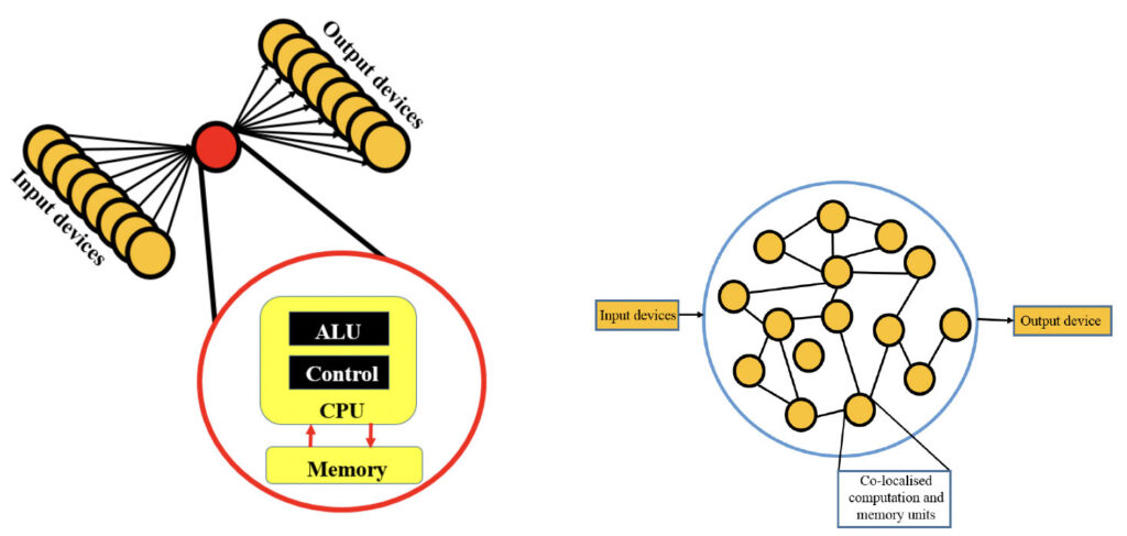
A graphical comparison of the von Neumann and Neuromorphic architecture. Left: The von Neumann architecture used in traditional computers. The red lines depict the data communication bottleneck in the von Neumann architecture. Right: A graphical representation of a general neuromorphic architecture. In this architecture, the processing and memory is decentralized across different neuronal units(the yellow nodes) and synapses(the black lines connecting the nodes), creating a naturally parallel computing environment via the mesh-like structure. (Source: DOI: 10.1109/IS.2016.7737434) [downloaded from https://www.nanowerk.com/spotlight/spotid=62353.php]

Berger offers a very good overview and I recommend reading his February 13, 2023 essay on neuromorphic engineering with one proviso, Note: A link has been removed,

Many researchers in this field see memristors as a key device component for neuromorphic engineering. Memristor – or memory resistor – devices are non-volatile nanoelectronic memory devices that were first theorized [emphasis mine] by Leon Chua in the 1970’s. However, it was some thirty years later that the first practical device was fabricated in 2008 by a group led by Stanley Williams [sometimes cited as R. Stanley Williams] at HP Research Labs.

Chua wasn’t the first as he, himself, has noted. Chua arrived at his theory independently in the 1970s but Bernard Widrow theorized what he called a ‘memistor’ in the 1960s. In fact “Memristors: they are older than you think” is a May 22, 2012 posting which featured an article “Two centuries of memristors” by Themistoklis Prodromakis, Christofer Toumazou and Leon Chua published in Nature Materials.

Most of us try to get it right but we don’t always succeed. It’s always good practice to read everyone (including me) with a little skepticism.
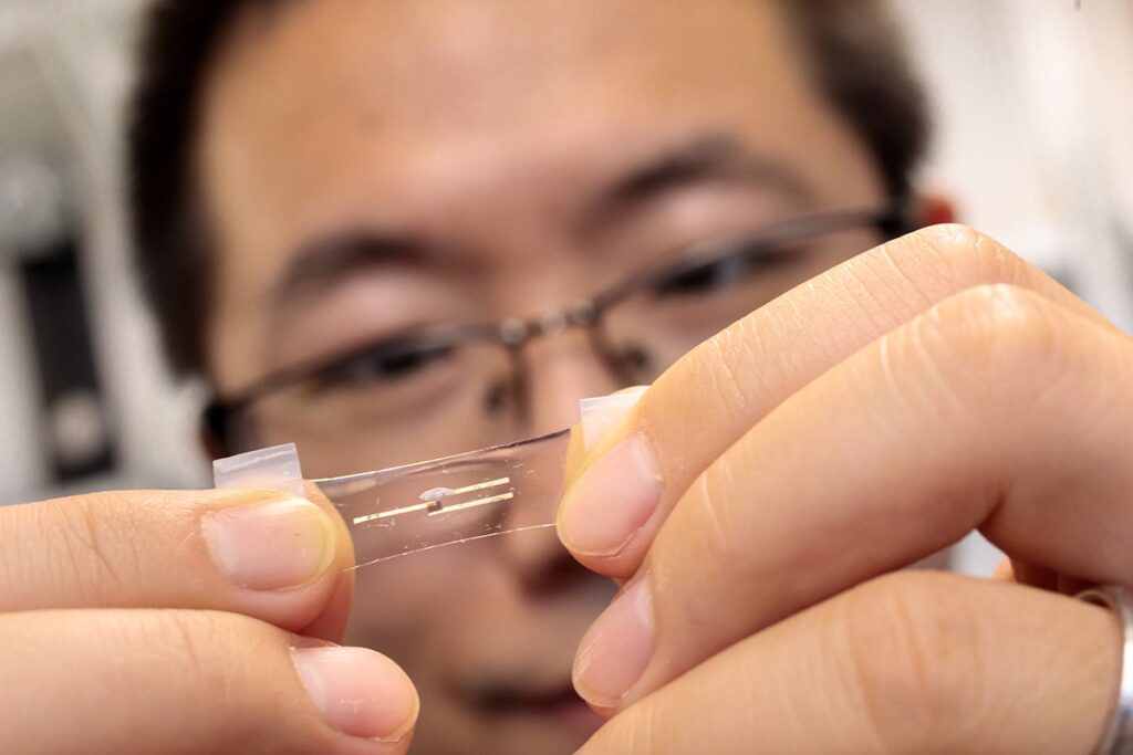
Combining silicon with metal oxide memristors to create powerful, low-energy intensive chips enabling AI in portable devices

In this one week, I’m publishing my first stories (see also June 13, 2023 posting “ChatGPT and a neuromorphic [brainlike] synapse“) where artificial intelligence (AI) software is combined with a memristor (hardware component) for brainlike (neuromorphic) computing.

Here’s more about some of the latest research from a March 30, 2023 news item on ScienceDaily,

Everyone is talking about the newest AI and the power of neural networks, forgetting that software is limited by the hardware on which it runs. But it is hardware, says USC [University of Southern California] Professor of Electrical and Computer Engineering Joshua Yang, that has become “the bottleneck.” Now, Yang’s new research with collaborators might change that. They believe that they have developed a new type of chip with the best memory of any chip thus far for edge AI (AI in portable devices).

A March 29, 2023 University of Southern California (USC) news release (also on EurekAlert), which originated the news item, contextualizes the research and delves further into the topic of neuromorphic hardware,

For approximately the past 30 years, while the size of the neural networks needed for AI and data science applications doubled every 3.5 months, the hardware capability needed to process them doubled only every 3.5 years. According to Yang, hardware presents a more and more severe problem for which few have patience. 

Governments, industry, and academia are trying to address this hardware challenge worldwide. Some continue to work on hardware solutions with silicon chips, while others are experimenting with new types of materials and devices.  Yang’s work falls into the middle—focusing on exploiting and combining the advantages of the new materials and traditional silicon technology that could support heavy AI and data science computation. 

Their new paper in Nature focuses on the understanding of fundamental physics that leads to a drastic increase in memory capacity needed for AI hardware. The team led by Yang, with researchers from USC (including Han Wang’s group), MIT [Massachusetts Institute of Technology], and the University of Massachusetts, developed a protocol for devices to reduce “noise” and demonstrated the practicality of using this protocol in integrated chips. This demonstration was made at TetraMem, a startup company co-founded by Yang and his co-authors  (Miao Hu, Qiangfei Xia, and Glenn Ge), to commercialize AI acceleration technology. According to Yang, this new memory chip has the highest information density per device (11 bits) among all types of known memory technologies thus far. Such small but powerful devices could play a critical role in bringing incredible power to the devices in our pockets. The chips are not just for memory but also for the processor. And millions of them in a small chip, working in parallel to rapidly run your AI tasks, could only require a small battery to power it. 

The chips that Yang and his colleagues are creating combine silicon with metal oxide memristors in order to create powerful but low-energy intensive chips. The technique focuses on using the positions of atoms to represent information rather than the number of electrons (which is the current technique involved in computations on chips). The positions of the atoms offer a compact and stable way to store more information in an analog, instead of digital fashion. Moreover, the information can be processed where it is stored instead of being sent to one of the few dedicated ‘processors,’ eliminating the so-called ‘von Neumann bottleneck’ existing in current computing systems.  In this way, says Yang, computing for AI is “more energy efficient with a higher throughput.”

How it works: 

Yang explains that electrons which are manipulated in traditional chips, are “light.” And this lightness, makes them prone to moving around and being more volatile.  Instead of storing memory through electrons, Yang and collaborators are storing memory in full atoms. Here is why this memory matters. Normally, says Yang, when one turns off a computer, the information memory is gone—but if you need that memory to run a new computation and your computer needs the information all over again, you have lost both time and energy.  This new method, focusing on activating atoms rather than electrons, does not require battery power to maintain stored information. Similar scenarios happen in AI computations, where a stable memory capable of high information density is crucial. Yang imagines this new tech that may enable powerful AI capability in edge devices, such as Google Glasses, which he says previously suffered from a frequent recharging issue.

Further, by converting chips to rely on atoms as opposed to electrons, chips become smaller.  Yang adds that with this new method, there is more computing capacity at a smaller scale. And this method, he says, could offer “many more levels of memory to help increase information density.” 

To put it in context, right now, ChatGPT is running on a cloud. The new innovation, followed by some further development, could put the power of a mini version of ChatGPT in everyone’s personal device. It could make such high-powered tech more affordable and accessible for all sorts of applications. 

Here’s a link to and a citation for the paper,

Thousands of conductance levels in memristors integrated on CMOS by Mingyi Rao, Hao Tang, Jiangbin Wu, Wenhao Song, Max Zhang, Wenbo Yin, Ye Zhuo, Fatemeh Kiani, Benjamin Chen, Xiangqi Jiang, Hefei Liu, Hung-Yu Chen, Rivu Midya, Fan Ye, Hao Jiang, Zhongrui Wang, Mingche Wu, Miao Hu, Han Wang, Qiangfei Xia, Ning Ge, Ju Li & J. Joshua Yang. Nature volume 615, pages 823–829 (2023) DOI: https://doi.org/10.1038/s41586-023-05759-5 Issue Date: 30 March 2023 Published: 29 March 2023

This paper is behind a paywall.

ChatGPT and a neuromorphic (brainlike) synapse

I was teaching an introductory course about nanotechnology back in 2014 and, at the end of a session, stated (more or less) that the full potential for artificial intelligence (software) wasn’t going to be perceived until the hardware (memistors) was part of the package. (It’s interesting to revisit that in light of the recent uproar around AI (covered in my May 25, 2023 posting, which offered a survey of the situation.)

One of the major problems with artificial intelligence is its memory. The other is energy consumption. Both problems could be addressed by the integration of memristors into the hardware, giving rise to neuromorphic (brainlike) computing. (For those who don’t know, the human brain in addition to its capacity for memory is remarkably energy efficient.)

This is the first time I’ve seen research into memristors where software has been included. Disclaimer: There may be a lot more research of this type; I just haven’t seen it before. A March 24, 2023 news item on ScienceDaily announces research from Korea,

ChatGPT’s impact extends beyond the education sector and is causing significant changes in other areas. The AI language model is recognized for its ability to perform various tasks, including paper writing, translation, coding, and more, all through question-and-answer-based interactions. The AI system relies on deep learning, which requires extensive training to minimize errors, resulting in frequent data transfers between memory and processors. However, traditional digital computer systems’ von Neumann architecture separates the storage and computation of information, resulting in increased power consumption and significant delays in AI computations. Researchers have developed semiconductor technologies suitable for AI applications to address this challenge.

A March 24, 2023 Pohang University of Science & Technology (POSTECH) press release (also on EurekAlert), which originated the news item, provides more detail,

A research team at POSTECH, led by Professor Yoonyoung Chung (Department of Electrical Engineering, Department of Semiconductor Engineering), Professor Seyoung Kim (Department of Materials Science and Engineering, Department of Semiconductor Engineering), and Ph.D. candidate Seongmin Park (Department of Electrical Engineering), has developed a high-performance AI semiconductor device [emphasis mine] using indium gallium zinc oxide (IGZO), an oxide semiconductor widely used in OLED [organic light-emitting diode] displays. The new device has proven to be excellent in terms of performance and power efficiency.

Efficient AI operations, such as those of ChatGPT, require computations to occur within the memory responsible for storing information. Unfortunately, previous AI semiconductor technologies were limited in meeting all the requirements, such as linear and symmetric programming and uniformity, to improve AI accuracy.

The research team sought IGZO as a key material for AI computations that could be mass-produced and provide uniformity, durability, and computing accuracy. This compound comprises four atoms in a fixed ratio of indium, gallium, zinc, and oxygen and has excellent electron mobility and leakage current properties, which have made it a backplane of the OLED display.

Using this material, the researchers developed a novel synapse device [emphasis mine] composed of two transistors interconnected through a storage node. The precise control of this node’s charging and discharging speed has enabled the AI semiconductor to meet the diverse performance metrics required for high-level performance. Furthermore, applying synaptic devices to a large-scale AI system requires the output current of synaptic devices to be minimized. The researchers confirmed the possibility of utilizing the ultra-thin film insulators inside the transistors to control the current, making them suitable for large-scale AI.

The researchers used the newly developed synaptic device to train and classify handwritten data, achieving a high accuracy of over 98%, [emphasis mine] which verifies its potential application in high-accuracy AI systems in the future.

Professor Chung explained, “The significance of my research team’s achievement is that we overcame the limitations of conventional AI semiconductor technologies that focused solely on material development. To do this, we utilized materials already in mass production. Furthermore, Linear and symmetrical programming characteristics were obtained through a new structure using two transistors as one synaptic device. Thus, our successful development and application of this new AI semiconductor technology show great potential to improve the efficiency and accuracy of AI.”

This study was published last week [March 2023] on the inside back cover of Advanced Electronic Materials [paper edition] and was supported by the Next-Generation Intelligent Semiconductor Technology Development Program through the National Research Foundation, funded by the Ministry of Science and ICT [Information and Communication Technologies] of Korea.

Here’s a link to and a citation for the paper,

Highly Linear and Symmetric Analog Neuromorphic Synapse Based on Metal Oxide Semiconductor Transistors with Self-Assembled Monolayer for High-Precision Neural Network Computatio by Seongmin Park, Suwon Seong, Gilsu Jeon, Wonjae Ji, Kyungmi Noh, Seyoung Kim, Yoonyoung Chun. Volume 9, Issue 3 March 2023 2200554 DOI: https://doi.org/10.1002/aelm.202200554 First published online: 29 December 2022

This paper is open access.

Also, there is another approach to using materials such as indium gallium zinc oxide (IGZO) for a memristor. That would be using biological cells as my June 6, 2023 posting, which features work on biological neural networks (BNNs), suggests in relation to creating robots that can perform brainlike computing.

Studying quantum conductance in memristive devices

A September 27, 2022 news item on phys.org provides an introduction to the later discussion of quantum effects in memristors,

At the nanoscale, the laws of classical physics suddenly become inadequate to explain the behavior of matter. It is precisely at this juncture that quantum theory comes into play, effectively describing the physical phenomena characteristic of the atomic and subatomic world. Thanks to the different behavior of matter on these length and energy scales, it is possible to develop new materials, devices and technologies based on quantum effects, which could yield a real quantum revolution that promises to innovate areas such as cryptography, telecommunications and computation.

The physics of very small objects, already at the basis of many technologies that we use today, is intrinsically linked to the world of nanotechnologies, the branch of applied science dealing with the control of matter at the nanometer scale (a nanometer is one billionth of a meter). This control of matter at the nanoscale is at the basis of the development of new electronic devices.

A September 27, 2022 Istituto Nazionale di Ricerca Metrologica (INRIM) press release (summary, PDF, and also on EurekAlert), which originated the news item, provides more information about the research,

Among these, memrisistors are considered promising devices for the realization of new computational architectures emulating functions of our brain, allowing the creation of increasingly efficient computation systems suitable for the development of the entire artificial intelligence sector, as recently shown by INRiM researchers in collaboration with several international universities and research institutes [1,2].

In this context, the EMPIR MEMQuD project, coordinated by INRiM, aims to study the quantum effects in such devices in which the electronic conduction properties can be manipulated allowing the observation of quantized conductivity phenomena at room temperature. In addition to analyzing the fundamentals and recent developments, the review work “Quantum Conductance in Memristive Devices: Fundamentals, Developments, and Applications” recently published in the prestigious international journal Advanced Materials (https://doi.org/10.1002/adma.202201248) analyzes how these effects can be used for a wide range of applications, from metrology to the development of next-generation memories and artificial intelligence.

Here’s a link to and a citation for the paper,

Quantum Conductance in Memristive Devices: Fundamentals, Developments, and Applications by Gianluca Milano, Masakazu Aono, Luca Boarino, Umberto Celano, Tsuyoshi Hasegawa, Michael Kozicki, Sayani Majumdar, Mariela Menghini, Enrique Miranda, Carlo Ricciardi, Stefan Tappertzhofen, Kazuya Terabe, Ilia Valov. Advanced Materials Volume 34, Issue32 August 11, 2022 2201248 DOI: https://doi.org/10.1002/adma.202201248 First published: 11 April 2022

This paper is open access.

You can find the EMPIR (European Metrology Programme for Innovation and Research) MEMQuD (quantum effects in memristive devices) project here, from the homepage,

Memristive devices are electrical resistance switches that couple ionics (i.e. dynamics of ions) with electronics. These devices offer a promising platform to observe quantum effects in air, at room temperature, and without an applied magnetic field. For this reason, they can be traced to fundamental physics constants fixed in the revised International System of Units (SI) for the realization of a quantum-based standard of resistance. However, as an emerging technology, memristive devices lack standardization and insights into the fundamental physics underlying its working principles.

The overall aim of the project is to investigate and exploit quantized conductance effects in memristive devices that operate reliably, in air and at room temperature. In particular, the project will focus on the development of memristive model systems and nanometrological characterization techniques at the nanoscale level of memristive devices, in order to better understand and control the quantized effects in memristive devices. Such an outcome would enable not only the development of neuromorphic systems but also the realization of a standard of resistance implementable on-chip for self-calibrating systems with zero-chain traceability in the spirit of the revised SI.

I’m starting to see mention of ‘neuromorphic computing’ in advertisements (specifically a Mercedes Benz car). I will have more about these first mentions of neuromorphic computing in consumer products in a future posting.

Skin-like computing device analyzes health data with brain-mimicking artificial intelligence (a neuromorphic chip)

The wearable neuromorphic chip, made of stretchy semiconductors, can implement artificial intelligence (AI) to process massive amounts of health information in real time. Above, Asst. Prof. Sihong Wang shows a single neuromorphic device with three electrodes. (Photo by John Zich)

Does everything have to be ‘brainy’? Read on for the latest on ‘brainy’ devices.

An August 4, 2022 University of Chicago news release (also on EurekAlert) describes work on a stretchable neuromorphic chip, Note: Links have been removed,

It’s a brainy Band-Aid, a smart watch without the watch, and a leap forward for wearable health technologies. Researchers at the University of Chicago’s Pritzker School of Molecular Engineering (PME) have developed a flexible, stretchable computing chip that processes information by mimicking the human brain. The device, described in the journal Matter, aims to change the way health data is processed.

“With this work we’ve bridged wearable technology with artificial intelligence and machine learning to create a powerful device which can analyze health data right on our own bodies,” said Sihong Wang, a materials scientist and Assistant Professor of Molecular Engineering.

Today, getting an in-depth profile about your health requires a visit to a hospital or clinic. In the future, Wang said, people’s health could be tracked continuously by wearable electronics that can detect disease even before symptoms appear. Unobtrusive, wearable computing devices are one step toward making this vision a reality. 

A Data Deluge
The future of healthcare that Wang—and many others—envision includes wearable biosensors to track complex indicators of health including levels of oxygen, sugar, metabolites and immune molecules in people’s blood. One of the keys to making these sensors feasible is their ability to conform to the skin. As such skin-like wearable biosensors emerge and begin collecting more and more information in real-time, the analysis becomes exponentially more complex. A single piece of data must be put into the broader perspective of a patient’s history and other health parameters.

Today’s smart phones are not capable of the kind of complex analysis required to learn a patient’s baseline health measurements and pick out important signals of disease. However, cutting-edge artificial intelligence platforms that integrate machine learning to identify patterns in extremely complex datasets can do a better job. But sending information from a device to a centralized AI location is not ideal.

“Sending health data wirelessly is slow and presents a number of privacy concerns,” he said. “It is also incredibly energy inefficient; the more data we start collecting, the more energy these transmissions will start using.”

Skin and Brains
Wang’s team set out to design a chip that could collect data from multiple biosensors and draw conclusions about a person’s health using cutting-edge machine learning approaches. Importantly, they wanted it to be wearable on the body and integrate seamlessly with skin.

“With a smart watch, there’s always a gap,” said Wang. “We wanted something that can achieve very intimate contact and accommodate the movement of skin.”

Wang and his colleagues turned to polymers, which can be used to build semiconductors and electrochemical transistors but also have the ability to stretch and bend. They assembled polymers into a device that allowed the artificial-intelligence-based analysis of health data. Rather than work like a typical computer, the chip— called a neuromorphic computing chip—functions more like a human brain, able to both store and analyze data in an integrated way.

Testing the Technology
To test the utility of their new device, Wang’s group used it to analyze electrocardiogram (ECG) data representing the electrical activity of the human heart. They trained the device to classify ECGs into five categories—healthy or four types of abnormal signals. Then, they tested it on new ECGs. Whether or not the chip was stretched or bent, they showed, it could accurately classify the heartbeats.

More work is needed to test the power of the device in deducing patterns of health and disease. But eventually, it could be used either to send patients or clinicians alerts, or to automatically tweak medications.

“If you can get real-time information on blood pressure, for instance, this device could very intelligently make decisions about when to adjust the patient’s blood pressure medication levels,” said Wang. That kind of automatic feedback loop is already used by some implantable insulin pumps, he added.

He already is planning new iterations of the device to both expand the type of devices with which it can integrate and the types of machine learning algorithms it uses.

“Integration of artificial intelligence with wearable electronics is becoming a very active landscape,” said Wang. “This is not finished research, it’s just a starting point.”

Here’s a link to and a citation for the paper,

Intrinsically stretchable neuromorphic devices for on-body processing of health data with artificial intelligence by Shilei Dai, Yahao Dai, Zixuan Zhao, Jie Xu, Jia Huang, Sihong Wang. Matter DOI:https://doi.org/10.1016/j.matt.2022.07.016 Published: August 04, 2022

This paper is behind a paywall.

New chip for neuromorphic computing runs at a fraction of the energy of today’s systems

An August 17, 2022 news item on Nanowerk announces big (so to speak) claims from a team researching neuromorphic (brainlike) computer chips,

An international team of researchers has designed and built a chip that runs computations directly in memory and can run a wide variety of artificial intelligence (AI) applications–all at a fraction of the energy consumed by computing platforms for general-purpose AI computing.

The NeuRRAM neuromorphic chip brings AI a step closer to running on a broad range of edge devices, disconnected from the cloud, where they can perform sophisticated cognitive tasks anywhere and anytime without relying on a network connection to a centralized server. Applications abound in every corner of the world and every facet of our lives, and range from smart watches, to VR headsets, smart earbuds, smart sensors in factories and rovers for space exploration.

The NeuRRAM chip is not only twice as energy efficient as the state-of-the-art “compute-in-memory” chips, an innovative class of hybrid chips that runs computations in memory, it also delivers results that are just as accurate as conventional digital chips. Conventional AI platforms are a lot bulkier and typically are constrained to using large data servers operating in the cloud.

In addition, the NeuRRAM chip is highly versatile and supports many different neural network models and architectures. As a result, the chip can be used for many different applications, including image recognition and reconstruction as well as voice recognition.

..

An August 17, 2022 University of California at San Diego (UCSD) news release (also on EurekAlert), which originated the news item, provides more detail than usually found in a news release,

“The conventional wisdom is that the higher efficiency of compute-in-memory is at the cost of versatility, but our NeuRRAM chip obtains efficiency while not sacrificing versatility,” said Weier Wan, the paper’s first corresponding author and a recent Ph.D. graduate of Stanford University who worked on the chip while at UC San Diego, where he was co-advised by Gert Cauwenberghs in the Department of Bioengineering. 

The research team, co-led by bioengineers at the University of California San Diego, presents their results in the Aug. 17 [2022] issue of Nature.

Currently, AI computing is both power hungry and computationally expensive. Most AI applications on edge devices involve moving data from the devices to the cloud, where the AI processes and analyzes it. Then the results are moved back to the device. That’s because most edge devices are battery-powered and as a result only have a limited amount of power that can be dedicated to computing. 

By reducing power consumption needed for AI inference at the edge, this NeuRRAM chip could lead to more robust, smarter and accessible edge devices and smarter manufacturing. It could also lead to better data privacy as the transfer of data from devices to the cloud comes with increased security risks. 

On AI chips, moving data from memory to computing units is one major bottleneck. 

“It’s the equivalent of doing an eight-hour commute for a two-hour work day,” Wan said. 

To solve this data transfer issue, researchers used what is known as resistive random-access memory, a type of non-volatile memory that allows for computation directly within memory rather than in separate computing units. RRAM and other emerging memory technologies used as synapse arrays for neuromorphic computing were pioneered in the lab of Philip Wong, Wan’s advisor at Stanford and a main contributor to this work. Computation with RRAM chips is not necessarily new, but generally it leads to a decrease in the accuracy of the computations performed on the chip and a lack of flexibility in the chip’s architecture. 

“Compute-in-memory has been common practice in neuromorphic engineering since it was introduced more than 30 years ago,” Cauwenberghs said.  “What is new with NeuRRAM is that the extreme efficiency now goes together with great flexibility for diverse AI applications with almost no loss in accuracy over standard digital general-purpose compute platforms.”

A carefully crafted methodology was key to the work with multiple levels of “co-optimization” across the abstraction layers of hardware and software, from the design of the chip to its configuration to run various AI tasks. In addition, the team made sure to account for various constraints that span from memory device physics to circuits and network architecture. 

“This chip now provides us with a platform to address these problems across the stack from devices and circuits to algorithms,” said Siddharth Joshi, an assistant professor of computer science and engineering at the University of Notre Dame , who started working on the project as a Ph.D. student and postdoctoral researcher in Cauwenberghs lab at UC San Diego. 

Chip performance

Researchers measured the chip’s energy efficiency by a measure known as energy-delay product, or EDP. EDP combines both the amount of energy consumed for every operation and the amount of times it takes to complete the operation. By this measure, the NeuRRAM chip achieves 1.6 to 2.3 times lower EDP (lower is better) and 7 to 13 times higher computational density than state-of-the-art chips. 

Researchers ran various AI tasks on the chip. It achieved 99% accuracy on a handwritten digit recognition task; 85.7% on an image classification task; and 84.7% on a Google speech command recognition task. In addition, the chip also achieved a 70% reduction in image-reconstruction error on an image-recovery task. These results are comparable to existing digital chips that perform computation under the same bit-precision, but with drastic savings in energy. 

Researchers point out that one key contribution of the paper is that all the results featured are obtained directly on the hardware. In many previous works of compute-in-memory chips, AI benchmark results were often obtained partially by software simulation. 

Next steps include improving architectures and circuits and scaling the design to more advanced technology nodes. Researchers also plan to tackle other applications, such as spiking neural networks.

“We can do better at the device level, improve circuit design to implement additional features and address diverse applications with our dynamic NeuRRAM platform,” said Rajkumar Kubendran, an assistant professor for the University of Pittsburgh, who started work on the project while a Ph.D. student in Cauwenberghs’ research group at UC San Diego.

In addition, Wan is a founding member of a startup that works on productizing the compute-in-memory technology. “As a researcher and  an engineer, my ambition is to bring research innovations from labs into practical use,” Wan said. 

New architecture 

The key to NeuRRAM’s energy efficiency is an innovative method to sense output in memory. Conventional approaches use voltage as input and measure current as the result. But this leads to the need for more complex and more power hungry circuits. In NeuRRAM, the team engineered a neuron circuit that senses voltage and performs analog-to-digital conversion in an energy efficient manner. This voltage-mode sensing can activate all the rows and all the columns of an RRAM array in a single computing cycle, allowing higher parallelism. 

In the NeuRRAM architecture, CMOS neuron circuits are physically interleaved with RRAM weights. It differs from conventional designs where CMOS circuits are typically on the peripheral of RRAM weights.The neuron’s connections with the RRAM array can be configured to serve as either input or output of the neuron. This allows neural network inference in various data flow directions without incurring overheads in area or power consumption. This in turn makes the architecture easier to reconfigure. 

To make sure that accuracy of the AI computations can be preserved across various neural network architectures, researchers developed a set of hardware algorithm co-optimization techniques. The techniques were verified on various neural networks including convolutional neural networks, long short-term memory, and restricted Boltzmann machines. 

As a neuromorphic AI chip, NeuroRRAM performs parallel distributed processing across 48 neurosynaptic cores. To simultaneously achieve high versatility and high efficiency, NeuRRAM supports data-parallelism by mapping a layer in the neural network model onto multiple cores for parallel inference on multiple data. Also, NeuRRAM offers model-parallelism by mapping different layers of a model onto different cores and performing inference in a pipelined fashion.

An international research team

The work is the result of an international team of researchers. 

The UC San Diego team designed the CMOS circuits that implement the neural functions interfacing with the RRAM arrays to support the synaptic functions in the chip’s architecture, for high efficiency and versatility. Wan, working closely with the entire team, implemented the design; characterized the chip; trained the AI models; and executed the experiments. Wan also developed a software toolchain that maps AI applications onto the chip. 

The RRAM synapse array and its operating conditions were extensively characterized and optimized at Stanford University. 

The RRAM array was fabricated and integrated onto CMOS at Tsinghua University. 

The Team at Notre Dame contributed to both the design and architecture of the chip and the subsequent machine learning model design and training.

The research started as part of the National Science Foundation funded Expeditions in Computing project on Visual Cortex on Silicon at Penn State University, with continued funding support from the Office of Naval Research Science of AI program, the Semiconductor Research Corporation and DARPA [{US} Defense Advanced Research Projects Agency] JUMP program, and Western Digital Corporation. 

Here’s a link to and a citation for the paper,

A compute-in-memory chip based on resistive random-access memory by Weier Wan, Rajkumar Kubendran, Clemens Schaefer, Sukru Burc Eryilmaz, Wenqiang Zhang, Dabin Wu, Stephen Deiss, Priyanka Raina, He Qian, Bin Gao, Siddharth Joshi, Huaqiang Wu, H.-S. Philip Wong & Gert Cauwenberghs. Nature volume 608, pages 504–512 (2022) DOI: https://doi.org/10.1038/s41586-022-04992-8 Published: 17 August 2022 Issue Date: 18 August 2022

This paper is open access.

Synaptic transistors for brainlike computers based on (more environmentally friendly) graphene

An August 9, 2022 news item on ScienceDaily describes research investigating materials other than silicon for neuromorphic (brainlike) computing purposes,

Computers that think more like human brains are inching closer to mainstream adoption. But many unanswered questions remain. Among the most pressing, what types of materials can serve as the best building blocks to unlock the potential of this new style of computing.

For most traditional computing devices, silicon remains the gold standard. However, there is a movement to use more flexible, efficient and environmentally friendly materials for these brain-like devices.

In a new paper, researchers from The University of Texas at Austin developed synaptic transistors for brain-like computers using the thin, flexible material graphene. These transistors are similar to synapses in the brain, that connect neurons to each other.

An August 8, 2022 University of Texas at Austin news release (also on EurekAlert but published August 9, 2022), which originated the news item, provides more detail about the research,

“Computers that think like brains can do so much more than today’s devices,” said Jean Anne Incorvia, an assistant professor in the Cockrell School of Engineering’s Department of Electrical and Computer Engineer and the lead author on the paper published today in Nature Communications. “And by mimicking synapses, we can teach these devices to learn on the fly, without requiring huge training methods that take up so much power.”

The Research: A combination of graphene and nafion, a polymer membrane material, make up the backbone of the synaptic transistor. Together, these materials demonstrate key synaptic-like behaviors — most importantly, the ability for the pathways to strengthen over time as they are used more often, a type of neural muscle memory. In computing, this means that devices will be able to get better at tasks like recognizing and interpreting images over time and do it faster.

Another important finding is that these transistors are biocompatible, which means they can interact with living cells and tissue. That is key for potential applications in medical devices that come into contact with the human body. Most materials used for these early brain-like devices are toxic, so they would not be able to contact living cells in any way.

Why It Matters: With new high-tech concepts like self-driving cars, drones and robots, we are reaching the limits of what silicon chips can efficiently do in terms of data processing and storage. For these next-generation technologies, a new computing paradigm is needed. Neuromorphic devices mimic processing capabilities of the brain, a powerful computer for immersive tasks.

“Biocompatibility, flexibility, and softness of our artificial synapses is essential,” said Dmitry Kireev, a post-doctoral researcher who co-led the project. “In the future, we envision their direct integration with the human brain, paving the way for futuristic brain prosthesis.”

Will It Really Happen: Neuromorphic platforms are starting to become more common. Leading chipmakers such as Intel and Samsung have either produced neuromorphic chips already or are in the process of developing them. However, current chip materials place limitations on what neuromorphic devices can do, so academic researchers are working hard to find the perfect materials for soft brain-like computers.

“It’s still a big open space when it comes to materials; it hasn’t been narrowed down to the next big solution to try,” Incorvia said. “And it might not be narrowed down to just one solution, with different materials making more sense for different applications.”

The Team: The research was led by Incorvia and Deji Akinwande, professor in the Department of Electrical and Computer Engineering. The two have collaborated many times together in the past, and Akinwande is a leading expert in graphene, using it in multiple research breakthroughs, most recently as part of a wearable electronic tattoo for blood pressure monitoring.

The idea for the project was conceived by Samuel Liu, a Ph.D. student and first author on the paper, in a class taught by Akinwande. Kireev then suggested the specific project. Harrison Jin, an undergraduate electrical and computer engineering student, measured the devices and analyzed data.

The team collaborated with T. Patrick Xiao and Christopher Bennett of Sandia National Laboratories, who ran neural network simulations and analyzed the resulting data.

Here’s a link to and a citation for the ‘graphene transistor’ paper,

Metaplastic and energy-efficient biocompatible graphene artificial synaptic transistors for enhanced accuracy neuromorphic computing by Dmitry Kireev, Samuel Liu, Harrison Jin, T. Patrick Xiao, Christopher H. Bennett, Deji Akinwande & Jean Anne C. Incorvia. Nature Communications volume 13, Article number: 4386 (2022) DOI: https://doi.org/10.1038/s41467-022-32078-6 Published: 28 July 2022

This paper is open access.

Neuromorphic computing and liquid-light interaction

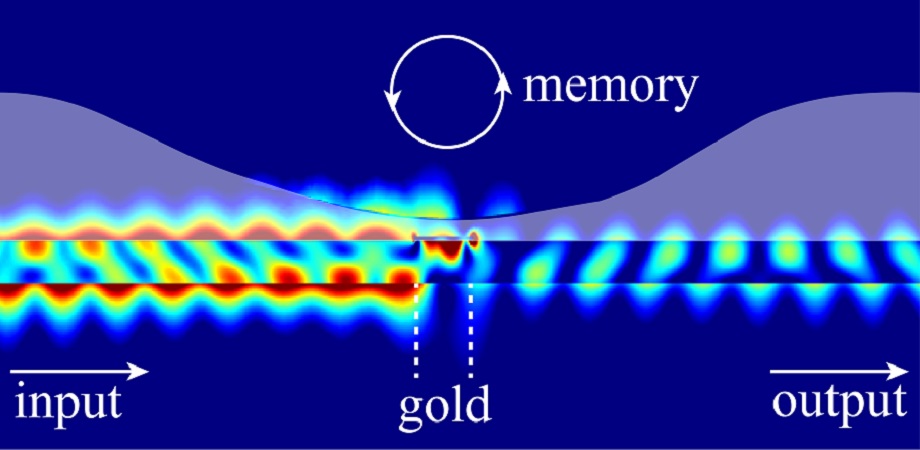
Simulation result of light affecting liquid geometry, which in turn affects reflection and transmission properties of the optical mode, thus constituting a two-way light–liquid interaction mechanism. The degree of deformation serves as an optical memory allowing to store the power magnitude of the previous optical pulse and use fluid dynamics to affect the subsequent optical pulse at the same actuation region, thus constituting an architecture where memory is part of the computation process. Credit: Gao et al., doi 10.1117/1.AP.4.4.046005

This is a fascinating approach to neuromorphic (brainlike) computing and given my recent post (August 29, 2022) about human cells being incorporated into computer chips, it’s part o my recent spate of posts about neuromorphic computing. From a July 25, 2022 news item on phys.org,

Sunlight sparkling on water evokes the rich phenomena of liquid-light interaction, spanning spatial and temporal scales. While the dynamics of liquids have fascinated researchers for decades, the rise of neuromorphic computing has sparked significant efforts to develop new, unconventional computational schemes based on recurrent neural networks, crucial to supporting wide range of modern technological applications, such as pattern recognition and autonomous driving. As biological neurons also rely on a liquid environment, a convergence may be attained by bringing nanoscale nonlinear fluid dynamics to neuromorphic computing.

A July 25, 2022 SPIE (International Society for Optics and Photonics) press release (also on EurekAlert), which originated the news item,

Researchers from University of California San Diego recently proposed a novel paradigm where liquids, which usually do not strongly interact with light on a micro- or nanoscale, support significant nonlinear response to optical fields. As reported in Advanced Photonics, the researchers predict a substantial light–liquid interaction effect through a proposed nanoscale gold patch operating as an optical heater and generating thickness changes in a liquid film covering the waveguide.

The liquid film functions as an optical memory. Here’s how it works: Light in the waveguide affects the geometry of the liquid surface, while changes in the shape of the liquid surface affect the properties of the optical mode in the waveguide, thus constituting a mutual coupling between the optical mode and the liquid film. Importantly, as the liquid geometry changes, the properties of the optical mode undergo a nonlinear response; after the optical pulse stops, the magnitude of liquid film’s deformation indicates the power of the previous optical pulse.

Remarkably, unlike traditional computational approaches, the nonlinear response and the memory reside at the same spatial region, thus suggesting realization of a compact (beyond von-Neumann) architecture where memory and computational unit occupy the same space. The researchers demonstrate that the combination of memory and nonlinearity allow the possibility of “reservoir computing” capable of performing digital and analog tasks, such as nonlinear logic gates and handwritten image recognition.

Their model also exploits another significant liquid feature: nonlocality. This enables them to predict computation enhancement that is simply not possible in solid state material platforms with limited nonlocal spatial scale. Despite nonlocality, the model does not quite achieve the levels of modern solid-state optics-based reservoir computing systems, yet the work nonetheless presents a clear roadmap for future experimental works aiming to validate the predicted effects and explore intricate coupling mechanisms of various physical processes in a liquid environment for computation.

Using multiphysics simulations to investigate coupling between light, fluid dynamics, heat transport, and surface tension effects, the researchers predict a family of novel nonlinear and nonlocal optical effects. They go a step further by indicating how these can be used to realize versatile, nonconventional computational platforms. Taking advantage of a mature silicon photonics platform, they suggest improvements to state-of-the-art liquid-assisted computation platforms by around five orders magnitude in space and at least two orders of magnitude in speed.

Here’s a link to and a citation for the paper,

Thin liquid film as an optical nonlinear-nonlocal medium and memory element in integrated optofluidic reservoir computer by Chengkuan Gao, Prabhav Gaur, Shimon Rubin, Yeshaiahu Fainman. Advanced Photonics, 4(4), 046005 (2022). https://doi.org/10.1117/1.AP.4.4.046005 Published: 1 July 2022

This paper is open access.

Guide for memristive hardware design

An August 15 ,2022 news item on ScienceDaily announces a type of guide for memristive hardware design,

They are many times faster than flash memory and require significantly less energy: memristive memory cells could revolutionize the energy efficiency of neuromorphic [brainlike] computers. In these computers, which are modeled on the way the human brain works, memristive cells function like artificial synapses. Numerous groups around the world are working on the use of corresponding neuromorphic circuits — but often with a lack of understanding of how they work and with faulty models. Jülich researchers have now summarized the physical principles and models in a comprehensive review article in the renowned journal Advances in Physics.

An August 15, 2022 Forschungszentrum Juelich press release (also on EurekAlert), which originated the news item, describes two papers designed to help researchers better understand and design memristive hardware,

Certain tasks – such as recognizing patterns and language – are performed highly efficiently by a human brain, requiring only about one ten-thousandth of the energy of a conventional, so-called “von Neumann” computer. One of the reasons lies in the structural differences: In a von Neumann architecture, there is a clear separation between memory and processor, which requires constant moving of large amounts of data. This is time and energy consuming – the so-called von Neumann bottleneck. In the brain, the computational operation takes place directly in the data memory and the biological synapses perform the tasks of memory and processor at the same time.

In Jülich, scientists have been working for more than 15 years on special data storage devices and components that can have similar properties to the synapses in the human brain. So-called memristive memory devices, also known as memristors, are considered to be extremely fast, energy-saving and can be miniaturized very well down to the nanometer range. The functioning of memristive cells is based on a very special effect: Their electrical resistance is not constant, but can be changed and reset again by applying an external voltage, theoretically continuously. The change in resistance is controlled by the movement of oxygen ions. If these move out of the semiconducting metal oxide layer, the material becomes more conductive and the electrical resistance drops. This change in resistance can be used to store information.

The processes that can occur in cells are very complex and vary depending on the material system. Three researchers from the Jülich Peter Grünberg Institute – Prof. Regina Dittmann, Dr. Stephan Menzel, and Prof. Rainer Waser – have therefore compiled their research results in a detailed review article, “Nanoionic memristive phenomena in metal oxides: the valence change mechanism”. They explain in detail the various physical and chemical effects in memristors and shed light on the influence of these effects on the switching properties of memristive cells and their reliability.

“If you look at current research activities in the field of neuromorphic memristor circuits, they are often based on empirical approaches to material optimization,” said Rainer Waser, director at the Peter Grünberg Institute. “Our goal with our review article is to give researchers something to work with in order to enable insight-driven material optimization.” The team of authors worked on the approximately 200-page article for ten years and naturally had to keep incorporating advances in knowledge.

“The analogous functioning of memristive cells required for their use as artificial synapses is not the normal case. Usually, there are sudden jumps in resistance, generated by the mutual amplification of ionic motion and Joule heat,” explains Regina Dittmann of the Peter Grünberg Institute. “In our review article, we provide researchers with the necessary understanding of how to change the dynamics of the cells to enable an analog operating mode.”

“You see time and again that groups simulate their memristor circuits with models that don’t take into account high dynamics of the cells at all. These circuits will never work.” said Stephan Menzel, who leads modeling activities at the Peter Grünberg Institute and has developed powerful compact models that are now in the public domain (www.emrl.de/jart.html). “In our review article, we provide the basics that are extremely helpful for a correct use of our compact models.”

Roadmap neuromorphic computing

The “Roadmap of Neuromorphic Computing and Engineering”, which was published in May 2022, shows how neuromorphic computing can help to reduce the enormous energy consumption of IT globally. In it, researchers from the Peter Grünberg Institute (PGI-7), together with leading experts in the field, have compiled the various technological possibilities, computational approaches, learning algorithms and fields of application. 

According to the study, applications in the field of artificial intelligence, such as pattern recognition or speech recognition, are likely to benefit in a special way from the use of neuromorphic hardware. This is because they are based – much more so than classical numerical computing operations – on the shifting of large amounts of data. Memristive cells make it possible to process these gigantic data sets directly in memory without transporting them back and forth between processor and memory. This could reduce the energy efficiency of artificial neural networks by orders of magnitude.

Memristive cells can also be interconnected to form high-density matrices that enable neural networks to learn locally. This so-called edge computing thus shifts computations from the data center to the factory floor, the vehicle, or the home of people in need of care. Thus, monitoring and controlling processes or initiating rescue measures can be done without sending data via a cloud. “This achieves two things at the same time: you save energy, and at the same time, personal data and data relevant to security remain on site,” says Prof. Dittmann, who played a key role in creating the roadmap as editor.

Here’s a link to and a citation for the ‘roadmap’,

2022 roadmap on neuromorphic computing and engineering by Dennis V Christensen, Regina Dittmann, Bernabe Linares-Barranco, Abu Sebastian, Manuel Le Gallo, Andrea Redaelli, Stefan Slesazeck, Thomas Mikolajick, Sabina Spiga, Stephan Menzel, Ilia Valov, Gianluca Milano, Carlo Ricciardi, Shi-Jun Liang, Feng Miao, Mario Lanza, Tyler J Quill, Scott T Keene, Alberto Salleo, Julie Grollier, Danijela Marković, Alice Mizrahi, Peng Yao, J Joshua Yang, Giacomo Indiveri, John Paul Strachan, Suman Datta, Elisa Vianello, Alexandre Valentian, Johannes Feldmann, Xuan Li, Wolfram H P Pernice, Harish Bhaskaran, Steve Furber, Emre Neftci, Franz Scherr, Wolfgang Maass, Srikanth Ramaswamy, Jonathan Tapson, Priyadarshini Panda, Youngeun Kim, Gouhei Tanaka, Simon Thorpe, Chiara Bartolozzi, Thomas A Cleland, Christoph Posch, ShihChii Liu, Gabriella Panuccio, Mufti Mahmud, Arnab Neelim Mazumder, Morteza Hosseini, Tinoosh Mohsenin, Elisa Donati, Silvia Tolu, Roberto Galeazzi, Martin Ejsing Christensen, Sune Holm, Daniele Ielmini and N Pryds. Neuromorphic Computing and Engineering , Volume 2, Number 2 DOI: 10.1088/2634-4386/ac4a83 20 May 2022 • © 2022 The Author(s)

This paper is open access.

Here’s the most recent paper,

Nanoionic memristive phenomena in metal oxides: the valence change mechanism by Regina Dittmann, Stephan Menzel & Rainer Waser. Advances in Physics
Volume 70, 2021 – Issue 2 Pages 155-349 DOI: https://doi.org/10.1080/00018732.2022.2084006 Published online: 06 Aug 2022

This paper is behind a paywall.

Quantum memristors

This March 24, 2022 news item on Nanowerk announcing work on a quantum memristor seems to have had a rough translation from German to English,

In recent years, artificial intelligence has become ubiquitous, with applications such as speech interpretation, image recognition, medical diagnosis, and many more. At the same time, quantum technology has been proven capable of computational power well beyond the reach of even the world’s largest supercomputer.

Physicists at the University of Vienna have now demonstrated a new device, called quantum memristor, which may allow to combine these two worlds, thus unlocking unprecedented capabilities. The experiment, carried out in collaboration with the National Research Council (CNR) and the Politecnico di Milano in Italy, has been realized on an integrated quantum processor operating on single photons.

Caption: Abstract representation of a neural network which is made of photons and has memory capability potentially related to artificial intelligence. Credit: © Equinox Graphics, University of Vienna

A March 24, 2022 University of Vienna (Universität Wien) press release (also on EurekAlert), which originated the news item, explains why this work has an impact on artificial intelligence,

At the heart of all artificial intelligence applications are mathematical models called neural networks. These models are inspired by the biological structure of the human brain, made of interconnected nodes. Just like our brain learns by constantly rearranging the connections between neurons, neural networks can be mathematically trained by tuning their internal structure until they become capable of human-level tasks: recognizing our face, interpreting medical images for diagnosis, even driving our cars. Having integrated devices capable of performing the computations involved in neural networks quickly and efficiently has thus become a major research focus, both academic and industrial.

One of the major game changers in the field was the discovery of the memristor, made in 2008. This device changes its resistance depending on a memory of the past current, hence the name memory-resistor, or memristor. Immediately after its discovery, scientists realized that (among many other applications) the peculiar behavior of memristors was surprisingly similar to that of neural synapses. The memristor has thus become a fundamental building block of neuromorphic architectures.

A group of experimental physicists from the University of Vienna, the National Research Council (CNR) and the Politecnico di Milano led by Prof. Philip Walther and Dr. Roberto Osellame, have now demonstrated that it is possible to engineer a device that has the same behavior as a memristor, while acting on quantum states and being able to encode and transmit quantum information. In other words, a quantum memristor. Realizing such device is challenging because the dynamics of a memristor tends to contradict the typical quantum behavior. 

By using single photons, i.e. single quantum particles of lights, and exploiting their unique ability to propagate simultaneously in a superposition of two or more paths, the physicists have overcome the challenge. In their experiment, single photons propagate along waveguides laser-written on a glass substrate and are guided on a superposition of several paths. One of these paths is used to measure the flux of photons going through the device and this quantity, through a complex electronic feedback scheme, modulates the transmission on the other output, thus achieving the desired memristive behavior. Besides demonstrating the quantum memristor, the researchers have provided simulations showing that optical networks with quantum memristor can be used to learn on both classical and quantum tasks, hinting at the fact that the quantum memristor may be the missing link between artificial intelligence and quantum computing.

“Unlocking the full potential of quantum resources within artificial intelligence is one of the greatest challenges of the current research in quantum physics and computer science”, says Michele Spagnolo, who is first author of the publication in the journal “Nature Photonics”. The group of Philip Walther of the University of Vienna has also recently demonstrated that robots can learn faster when using quantum resources and borrowing schemes from quantum computation. This new achievement represents one more step towards a future where quantum artificial intelligence become reality.

Here’s a link to and a citation for the paper,

Experimental photonic quantum memristor by Michele Spagnolo, Joshua Morris, Simone Piacentini, Michael Antesberger, Francesco Massa, Andrea Crespi, Francesco Ceccarelli, Roberto Osellame & Philip Walther. Nature Photonics volume 16, pages 318–323 (2022) DOI: https://doi.org/10.1038/s41566-022-00973-5 Published 24 March 2022 Issue Date April 2022

This paper is open access.