Tag Archives: neuromorphic engineering

Artificial synapse courtesy of nanowires

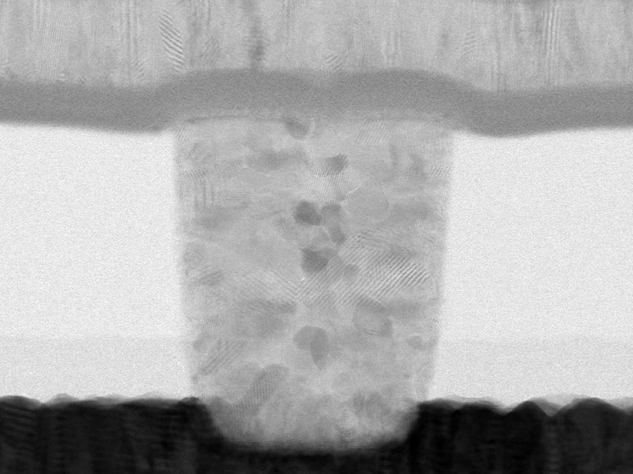
It looks like a popsicle to me,

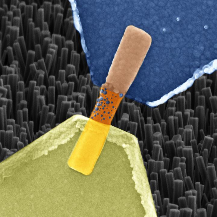
Caption: Image captured by an electron microscope of a single nanowire memristor (highlighted in colour to distinguish it from other nanowires in the background image). Blue: silver electrode, orange: nanowire, yellow: platinum electrode. Blue bubbles are dispersed over the nanowire. They are made up of silver ions and form a bridge between the electrodes which increases the resistance. Credit: Forschungszentrum Jülich

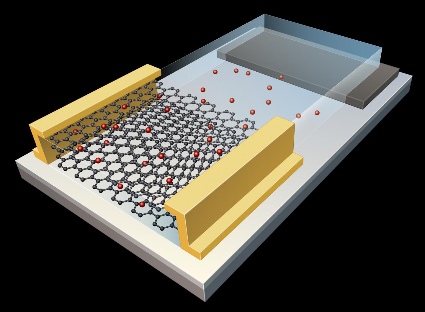
Not a popsicle but a representation of a device (memristor) scientists claim mimics a biological nerve cell according to a December 5, 2018 news item on ScienceDaily,

Scientists from Jülich [Germany] together with colleagues from Aachen [Germany] and Turin [Italy] have produced a memristive element made from nanowires that functions in much the same way as a biological nerve cell. The component is able to both save and process information, as well as receive numerous signals in parallel. The resistive switching cell made from oxide crystal nanowires is thus proving to be the ideal candidate for use in building bioinspired “neuromorphic” processors, able to take over the diverse functions of biological synapses and neurons.

A Dec. 5, 2018 Forschungszentrum Jülich press release (also on EurekAlert), which originated the news item, provides more details,

Computers have learned a lot in recent years. Thanks to rapid progress in artificial intelligence they are now able to drive cars, translate texts, defeat world champions at chess, and much more besides. In doing so, one of the greatest challenges lies in the attempt to artificially reproduce the signal processing in the human brain. In neural networks, data are stored and processed to a high degree in parallel. Traditional computers on the other hand rapidly work through tasks in succession and clearly distinguish between the storing and processing of information. As a rule, neural networks can only be simulated in a very cumbersome and inefficient way using conventional hardware.

Systems with neuromorphic chips that imitate the way the human brain works offer significant advantages. Experts in the field describe this type of bioinspired computer as being able to work in a decentralised way, having at its disposal a multitude of processors, which, like neurons in the brain, are connected to each other by networks. If a processor breaks down, another can take over its function. What is more, just like in the brain, where practice leads to improved signal transfer, a bioinspired processor should have the capacity to learn.

“With today’s semiconductor technology, these functions are to some extent already achievable. These systems are however suitable for particular applications and require a lot of space and energy,” says Dr. Ilia Valov from Forschungszentrum Jülich. “Our nanowire devices made from zinc oxide crystals can inherently process and even store information, as well as being extremely small and energy efficient,” explains the researcher from Jülich’s Peter Grünberg Institute.

For years memristive cells have been ascribed the best chances of being capable of taking over the function of neurons and synapses in bioinspired computers. They alter their electrical resistance depending on the intensity and direction of the electric current flowing through them. In contrast to conventional transistors, their last resistance value remains intact even when the electric current is switched off. Memristors are thus fundamentally capable of learning.

In order to create these properties, scientists at Forschungszentrum Jülich and RWTH Aachen University used a single zinc oxide nanowire, produced by their colleagues from the polytechnic university in Turin. Measuring approximately one ten-thousandth of a millimeter in size, this type of nanowire is over a thousand times thinner than a human hair. The resulting memristive component not only takes up a tiny amount of space, but also is able to switch much faster than flash memory.

Nanowires offer promising novel physical properties compared to other solids and are used among other things in the development of new types of solar cells, sensors, batteries and computer chips. Their manufacture is comparatively simple. Nanowires result from the evaporation deposition of specified materials onto a suitable substrate, where they practically grow of their own accord.

In order to create a functioning cell, both ends of the nanowire must be attached to suitable metals, in this case platinum and silver. The metals function as electrodes, and in addition, release ions triggered by an appropriate electric current. The metal ions are able to spread over the surface of the wire and build a bridge to alter its conductivity.

Components made from single nanowires are, however, still too isolated to be of practical use in chips. Consequently, the next step being planned by the Jülich and Turin researchers is to produce and study a memristive element, composed of a larger, relatively easy to generate group of several hundred nanowires offering more exciting functionalities.

The Italians have also written about the work in a December 4, 2018 news item for the Polytecnico di Torino’s inhouse magazine, PoliFlash’. I like the image they’ve used better as it offers a bit more detail and looks less like a popsicle. First, the image,

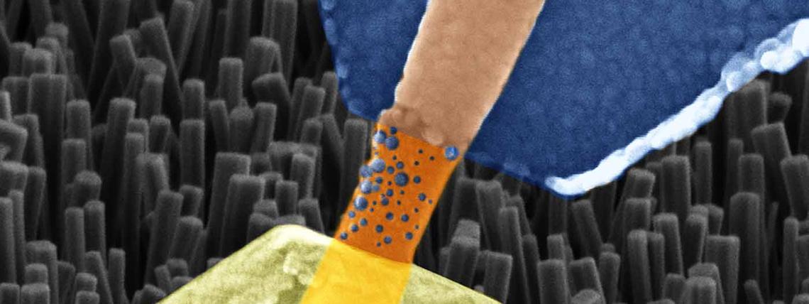
Courtesy: Polytecnico di Torino

Now, the news item, which includes some historical information about the memristor (Note: There is some repetition and links have been removed),

Emulating and understanding the human brain is one of the most important challenges for modern technology: on the one hand, the ability to artificially reproduce the processing of brain signals is one of the cornerstones for the development of artificial intelligence, while on the other the understanding of the cognitive processes at the base of the human mind is still far away.

And the research published in the prestigious journal Nature Communications by Gianluca Milano and Carlo Ricciardi, PhD student and professor, respectively, of the Applied Science and Technology Department of the Politecnico di Torino, represents a step forward in these directions. In fact, the study entitled “Self-limited single nanowire systems combining all-in-one memristive and neuromorphic functionalities” shows how it is possible to artificially emulate the activity of synapses, i.e. the connections between neurons that regulate the learning processes in our brain, in a single “nanowire” with a diameter thousands of times smaller than that of a hair.

It is a crystalline nanowire that takes the “memristor”, the electronic device able to artificially reproduce the functions of biological synapses, to a more performing level. Thanks to the use of nanotechnologies, which allow the manipulation of matter at the atomic level, it was for the first time possible to combine into one single device the synaptic functions that were individually emulated through specific devices. For this reason, the nanowire allows an extreme miniaturisation of the “memristor”, significantly reducing the complexity and energy consumption of the electronic circuits necessary for the implementation of learning algorithms.

Starting from the theorisation of the “memristor” in 1971 by Prof. Leon Chua – now visiting professor at the Politecnico di Torino, who was conferred an honorary degree by the University in 2015 – this new technology will not only allow smaller and more performing devices to be created for the implementation of increasingly “intelligent” computers, but is also a significant step forward for the emulation and understanding of the functioning of the brain.

“The nanowire memristor – said Carlo Ricciardirepresents a model system for the study of physical and electrochemical phenomena that govern biological synapses at the nanoscale. The work is the result of the collaboration between our research team and the RWTH University of Aachen in Germany, supported by INRiM, the National Institute of Metrological Research, and IIT, the Italian Institute of Technology.”

h.t for the Italian info. to Nanowerk’s Dec. 10, 2018 news item.

Here’s a link to and a citation for the paper,

Self-limited single nanowire systems combining all-in-one memristive and neuromorphic functionalities by Gianluca Milano, Michael Luebben, Zheng Ma, Rafal Dunin-Borkowski, Luca Boarino, Candido F. Pirri, Rainer Waser, Carlo Ricciardi, & Ilia Valov. Nature Communicationsvolume 9, Article number: 5151 (2018) DOI: https://doi.org/10.1038/s41467-018-07330-7 Published: 04 December 2018

This paper is open access.

Just use the search term “memristor” in the blog search engine if you’re curious about the multitudinous number of postings on the topic here.

Artificial synapse based on tantalum oxide from Korean researchers

This memristor story comes from South Korea as we progress on the way to neuromorphic computing (brainlike computing). A Sept. 7, 2018 news item on ScienceDaily makes the announcement,

A research team led by Director Myoung-Jae Lee from the Intelligent Devices and Systems Research Group at DGIST (Daegu Gyeongbuk Institute of Science and Technology) has succeeded in developing an artificial synaptic device that mimics the function of the nerve cells (neurons) and synapses that are response for memory in human brains. [sic]

Synapses are where axons and dendrites meet so that neurons in the human brain can send and receive nerve signals; there are known to be hundreds of trillions of synapses in the human brain.

This chemical synapse information transfer system, which transfers information from the brain, can handle high-level parallel arithmetic with very little energy, so research on artificial synaptic devices, which mimic the biological function of a synapse, is under way worldwide.

Dr. Lee’s research team, through joint research with teams led by Professor Gyeong-Su Park from Seoul National University; Professor Sung Kyu Park from Chung-ang University; and Professor Hyunsang Hwang from Pohang University of Science and Technology (POSTEC), developed a high-reliability artificial synaptic device with multiple values by structuring tantalum oxide — a trans-metallic material — into two layers of Ta2O5-x and TaO2-x and by controlling its surface.

A September 7, 2018 DGIST press release (also on EurekAlert), which originated the news item, delves further into the work,

The artificial synaptic device developed by the research team is an electrical synaptic device that simulates the function of synapses in the brain as the resistance of the tantalum oxide layer gradually increases or decreases depending on the strength of the electric signals. It has succeeded in overcoming durability limitations of current devices by allowing current control only on one layer of Ta2O5-x.

In addition, the research team successfully implemented an experiment that realized synapse plasticity [or synaptic plasticity], which is the process of creating, storing, and deleting memories, such as long-term strengthening of memory and long-term suppression of memory deleting by adjusting the strength of the synapse connection between neurons.

The non-volatile multiple-value data storage method applied by the research team has the technological advantage of having a small area of an artificial synaptic device system, reducing circuit connection complexity, and reducing power consumption by more than one-thousandth compared to data storage methods based on digital signals using 0 and 1 such as volatile CMOS (Complementary Metal Oxide Semiconductor).

The high-reliability artificial synaptic device developed by the research team can be used in ultra-low-power devices or circuits for processing massive amounts of big data due to its capability of low-power parallel arithmetic. It is expected to be applied to next-generation intelligent semiconductor device technologies such as development of artificial intelligence (AI) including machine learning and deep learning and brain-mimicking semiconductors.

Dr. Lee said, “This research secured the reliability of existing artificial synaptic devices and improved the areas pointed out as disadvantages. We expect to contribute to the development of AI based on the neuromorphic system that mimics the human brain by creating a circuit that imitates the function of neurons.”

Here’s a link to and a citation for the paper,

Reliable Multivalued Conductance States in TaOx Memristors through Oxygen Plasma-Assisted Electrode Deposition with in Situ-Biased Conductance State Transmission Electron Microscopy Analysis by Myoung-Jae Lee, Gyeong-Su Park, David H. Seo, Sung Min Kwon, Hyeon-Jun Lee, June-Seo Kim, MinKyung Jung, Chun-Yeol You, Hyangsook Lee, Hee-Goo Kim, Su-Been Pang, Sunae Seo, Hyunsang Hwang, and Sung Kyu Park. ACS Appl. Mater. Interfaces, 2018, 10 (35), pp 29757–29765 DOI: 10.1021/acsami.8b09046 Publication Date (Web): July 23, 2018

Copyright © 2018 American Chemical Society

This paper is open access.

You can find other memristor and neuromorphic computing stories here by using the search terms I’ve highlighted,  My latest (more or less) is an April 19, 2018 posting titled, New path to viable memristor/neuristor?

Finally, here’s an image from the Korean researchers that accompanied their work,

Caption: Representation of neurons and synapses in the human brain. The magnified synapse represents the portion mimicked using solid-state devices. Credit: Daegu Gyeongbuk Institute of Science and Technology(DGIST)

Bringing memristors to the masses and cutting down on energy use

One of my earliest posts featuring memristors (May 9, 2008) focused on their potential for energy savings but since then most of my postings feature research into their application in the field of neuromorphic (brainlike) computing. (For a description and abbreviated history of the memristor go to this page on my Nanotech Mysteries Wiki.)

In a sense this July 30, 2018 news item on Nanowerk is a return to the beginning,

A new way of arranging advanced computer components called memristors on a chip could enable them to be used for general computing, which could cut energy consumption by a factor of 100.

This would improve performance in low power environments such as smartphones or make for more efficient supercomputers, says a University of Michigan researcher.

“Historically, the semiconductor industry has improved performance by making devices faster. But although the processors and memories are very fast, they can’t be efficient because they have to wait for data to come in and out,” said Wei Lu, U-M professor of electrical and computer engineering and co-founder of memristor startup Crossbar Inc.

Memristors might be the answer. Named as a portmanteau of memory and resistor, they can be programmed to have different resistance states–meaning they store information as resistance levels. These circuit elements enable memory and processing in the same device, cutting out the data transfer bottleneck experienced by conventional computers in which the memory is separate from the processor.

A July 30, 2018 University of Michigan news release (also on EurekAlert), which originated the news item, expands on the theme,

… unlike ordinary bits, which are 1 or 0, memristors can have resistances that are on a continuum. Some applications, such as computing that mimics the brain (neuromorphic), take advantage of the analog nature of memristors. But for ordinary computing, trying to differentiate among small variations in the current passing through a memristor device is not precise enough for numerical calculations.

Lu and his colleagues got around this problem by digitizing the current outputs—defining current ranges as specific bit values (i.e., 0 or 1). The team was also able to map large mathematical problems into smaller blocks within the array, improving the efficiency and flexibility of the system.

Computers with these new blocks, which the researchers call “memory-processing units,” could be particularly useful for implementing machine learning and artificial intelligence algorithms. They are also well suited to tasks that are based on matrix operations, such as simulations used for weather prediction. The simplest mathematical matrices, akin to tables with rows and columns of numbers, can map directly onto the grid of memristors.

The memristor array situated on a circuit board.

The memristor array situated on a circuit board. Credit: Mohammed Zidan, Nanoelectronics group, University of Michigan.

Once the memristors are set to represent the numbers, operations that multiply and sum the rows and columns can be taken care of simultaneously, with a set of voltage pulses along the rows. The current measured at the end of each column contains the answers. A typical processor, in contrast, would have to read the value from each cell of the matrix, perform multiplication, and then sum up each column in series.

“We get the multiplication and addition in one step. It’s taken care of through physical laws. We don’t need to manually multiply and sum in a processor,” Lu said.

His team chose to solve partial differential equations as a test for a 32×32 memristor array—which Lu imagines as just one block of a future system. These equations, including those behind weather forecasting, underpin many problems science and engineering but are very challenging to solve. The difficulty comes from the complicated forms and multiple variables needed to model physical phenomena.

When solving partial differential equations exactly is impossible, solving them approximately can require supercomputers. These problems often involve very large matrices of data, so the memory-processor communication bottleneck is neatly solved with a memristor array. The equations Lu’s team used in their demonstration simulated a plasma reactor, such as those used for integrated circuit fabrication.

This work is described in a study, “A general memristor-based partial differential equation solver,” published in the journal Nature Electronics.

It was supported by the Defense Advanced Research Projects Agency (DARPA) (grant no. HR0011-17-2-0018) and by the National Science Foundation (NSF) (grant no. CCF-1617315).

Here’s a link and a citation for the paper,

A general memristor-based partial differential equation solver by Mohammed A. Zidan, YeonJoo Jeong, Jihang Lee, Bing Chen, Shuo Huang, Mark J. Kushner & Wei D. Lu. Nature Electronicsvolume 1, pages411–420 (2018) DOI: https://doi.org/10.1038/s41928-018-0100-6 Published: 13 July 2018

This paper is behind a paywall.

For the curious, Dr. Lu’s startup company, Crossbar can be found here.

If only AI had a brain (a Wizard of Oz reference?)

The title, which I’ve borrowed from the news release, is the only Wizard of Oz reference that I can find but it works so well, you don’t really need anything more.

Moving onto the news, a July 23, 2018 news item on phys.org announces new work on developing an artificial synapse (Note: A link has been removed),

Digital computation has rendered nearly all forms of analog computation obsolete since as far back as the 1950s. However, there is one major exception that rivals the computational power of the most advanced digital devices: the human brain.

The human brain is a dense network of neurons. Each neuron is connected to tens of thousands of others, and they use synapses to fire information back and forth constantly. With each exchange, the brain modulates these connections to create efficient pathways in direct response to the surrounding environment. Digital computers live in a world of ones and zeros. They perform tasks sequentially, following each step of their algorithms in a fixed order.

A team of researchers from Pitt’s [University of Pittsburgh] Swanson School of Engineering have developed an “artificial synapse” that does not process information like a digital computer but rather mimics the analog way the human brain completes tasks. Led by Feng Xiong, assistant professor of electrical and computer engineering, the researchers published their results in the recent issue of the journal Advanced Materials (DOI: 10.1002/adma.201802353). His Pitt co-authors include Mohammad Sharbati (first author), Yanhao Du, Jorge Torres, Nolan Ardolino, and Minhee Yun.

A July 23, 2018 University of Pittsburgh Swanson School of Engineering news release (also on EurekAlert), which originated the news item, provides further information,

“The analog nature and massive parallelism of the brain are partly why humans can outperform even the most powerful computers when it comes to higher order cognitive functions such as voice recognition or pattern recognition in complex and varied data sets,” explains Dr. Xiong.

An emerging field called “neuromorphic computing” focuses on the design of computational hardware inspired by the human brain. Dr. Xiong and his team built graphene-based artificial synapses in a two-dimensional honeycomb configuration of carbon atoms. Graphene’s conductive properties allowed the researchers to finely tune its electrical conductance, which is the strength of the synaptic connection or the synaptic weight. The graphene synapse demonstrated excellent energy efficiency, just like biological synapses.

In the recent resurgence of artificial intelligence, computers can already replicate the brain in certain ways, but it takes about a dozen digital devices to mimic one analog synapse. The human brain has hundreds of trillions of synapses for transmitting information, so building a brain with digital devices is seemingly impossible, or at the very least, not scalable. Xiong Lab’s approach provides a possible route for the hardware implementation of large-scale artificial neural networks.

According to Dr. Xiong, artificial neural networks based on the current CMOS (complementary metal-oxide semiconductor) technology will always have limited functionality in terms of energy efficiency, scalability, and packing density. “It is really important we develop new device concepts for synaptic electronics that are analog in nature, energy-efficient, scalable, and suitable for large-scale integrations,” he says. “Our graphene synapse seems to check all the boxes on these requirements so far.”

With graphene’s inherent flexibility and excellent mechanical properties, these graphene-based neural networks can be employed in flexible and wearable electronics to enable computation at the “edge of the internet”–places where computing devices such as sensors make contact with the physical world.

“By empowering even a rudimentary level of intelligence in wearable electronics and sensors, we can track our health with smart sensors, provide preventive care and timely diagnostics, monitor plants growth and identify possible pest issues, and regulate and optimize the manufacturing process–significantly improving the overall productivity and quality of life in our society,” Dr. Xiong says.

The development of an artificial brain that functions like the analog human brain still requires a number of breakthroughs. Researchers need to find the right configurations to optimize these new artificial synapses. They will need to make them compatible with an array of other devices to form neural networks, and they will need to ensure that all of the artificial synapses in a large-scale neural network behave in the same exact manner. Despite the challenges, Dr. Xiong says he’s optimistic about the direction they’re headed.

“We are pretty excited about this progress since it can potentially lead to the energy-efficient, hardware implementation of neuromorphic computing, which is currently carried out in power-intensive GPU clusters. The low-power trait of our artificial synapse and its flexible nature make it a suitable candidate for any kind of A.I. device, which would revolutionize our lives, perhaps even more than the digital revolution we’ve seen over the past few decades,” Dr. Xiong says.

There is a visual representation of this artificial synapse,

Caption: Pitt engineers built a graphene-based artificial synapse in a two-dimensional, honeycomb configuration of carbon atoms that demonstrated excellent energy efficiency comparable to biological synapses Credit: Swanson School of Engineering

Here’s a link to and a citation for the paper,

Low‐Power, Electrochemically Tunable Graphene Synapses for Neuromorphic Computing by Mohammad Taghi Sharbati, Yanhao Du, Jorge Torres, Nolan D. Ardolino, Minhee Yun, Feng Xiong. Advanced Materials DOP: https://doi.org/10.1002/adma.201802353 First published [online]: 23 July 2018

This paper is behind a paywall.

I did look at the paper and if I understand it rightly, this approach is different from the memristor-based approaches that I have so often featured here. More than that I cannot say.

Finally, the Wizard of Oz song ‘If I Only Had a Brain’,

Brainy and brainy: a novel synaptic architecture and a neuromorphic computing platform called SpiNNaker

I have two items about brainlike computing. The first item hearkens back to memristors, a topic I have been following since 2008. (If you’re curious about the various twists and turns just enter  the term ‘memristor’ in this blog’s search engine.) The latest on memristors is from a team than includes IBM (US), École Politechnique Fédérale de Lausanne (EPFL; Swizterland), and the New Jersey Institute of Technology (NJIT; US). The second bit comes from a Jülich Research Centre team in Germany and concerns an approach to brain-like computing that does not include memristors.

Multi-memristive synapses

In the inexorable march to make computers function more like human brains (neuromorphic engineering/computing), an international team has announced its latest results in a July 10, 2018 news item on Nanowerk,

Two New Jersey Institute of Technology (NJIT) researchers, working with collaborators from the IBM Research Zurich Laboratory and the École Polytechnique Fédérale de Lausanne, have demonstrated a novel synaptic architecture that could lead to a new class of information processing systems inspired by the brain.

The findings are an important step toward building more energy-efficient computing systems that also are capable of learning and adaptation in the real world. …

A July 10, 2018 NJIT news release (also on EurekAlert) by Tracey Regan, which originated by the news item, adds more details,

The researchers, Bipin Rajendran, an associate professor of electrical and computer engineering, and S. R. Nandakumar, a graduate student in electrical engineering, have been developing brain-inspired computing systems that could be used for a wide range of big data applications.

Over the past few years, deep learning algorithms have proven to be highly successful in solving complex cognitive tasks such as controlling self-driving cars and language understanding. At the heart of these algorithms are artificial neural networks – mathematical models of the neurons and synapses of the brain – that are fed huge amounts of data so that the synaptic strengths are autonomously adjusted to learn the intrinsic features and hidden correlations in these data streams.

However, the implementation of these brain-inspired algorithms on conventional computers is highly inefficient, consuming huge amounts of power and time. This has prompted engineers to search for new materials and devices to build special-purpose computers that can incorporate the algorithms. Nanoscale memristive devices, electrical components whose conductivity depends approximately on prior signaling activity, can be used to represent the synaptic strength between the neurons in artificial neural networks.

While memristive devices could potentially lead to faster and more power-efficient computing systems, they are also plagued by several reliability issues that are common to nanoscale devices. Their efficiency stems from their ability to be programmed in an analog manner to store multiple bits of information; however, their electrical conductivities vary in a non-deterministic and non-linear fashion.

In the experiment, the team showed how multiple nanoscale memristive devices exhibiting these characteristics could nonetheless be configured to efficiently implement artificial intelligence algorithms such as deep learning. Prototype chips from IBM containing more than one million nanoscale phase-change memristive devices were used to implement a neural network for the detection of hidden patterns and correlations in time-varying signals.

“In this work, we proposed and experimentally demonstrated a scheme to obtain high learning efficiencies with nanoscale memristive devices for implementing learning algorithms,” Nandakumar says. “The central idea in our demonstration was to use several memristive devices in parallel to represent the strength of a synapse of a neural network, but only chose one of them to be updated at each step based on the neuronal activity.”

Here’s a link to and a citation for the paper,

Neuromorphic computing with multi-memristive synapses by Irem Boybat, Manuel Le Gallo, S. R. Nandakumar, Timoleon Moraitis, Thomas Parnell, Tomas Tuma, Bipin Rajendran, Yusuf Leblebici, Abu Sebastian, & Evangelos Eleftheriou. Nature Communications volume 9, Article number: 2514 (2018) DOI: https://doi.org/10.1038/s41467-018-04933-y Published 28 June 2018

This is an open access paper.

Also they’ve got a couple of very nice introductory paragraphs which I’m including here, (from the June 28, 2018 paper in Nature Communications; Note: Links have been removed),

The human brain with less than 20 W of power consumption offers a processing capability that exceeds the petaflops mark, and thus outperforms state-of-the-art supercomputers by several orders of magnitude in terms of energy efficiency and volume. Building ultra-low-power cognitive computing systems inspired by the operating principles of the brain is a promising avenue towards achieving such efficiency. Recently, deep learning has revolutionized the field of machine learning by providing human-like performance in areas, such as computer vision, speech recognition, and complex strategic games1. However, current hardware implementations of deep neural networks are still far from competing with biological neural systems in terms of real-time information-processing capabilities with comparable energy consumption.

One of the reasons for this inefficiency is that most neural networks are implemented on computing systems based on the conventional von Neumann architecture with separate memory and processing units. There are a few attempts to build custom neuromorphic hardware that is optimized to implement neural algorithms2,3,4,5. However, as these custom systems are typically based on conventional silicon complementary metal oxide semiconductor (CMOS) circuitry, the area efficiency of such hardware implementations will remain relatively low, especially if in situ learning and non-volatile synaptic behavior have to be incorporated. Recently, a new class of nanoscale devices has shown promise for realizing the synaptic dynamics in a compact and power-efficient manner. These memristive devices store information in their resistance/conductance states and exhibit conductivity modulation based on the programming history6,7,8,9. The central idea in building cognitive hardware based on memristive devices is to store the synaptic weights as their conductance states and to perform the associated computational tasks in place.

The two essential synaptic attributes that need to be emulated by memristive devices are the synaptic efficacy and plasticity. …

It gets more complicated from there.

Now onto the next bit.

SpiNNaker

At a guess, those capitalized N’s are meant to indicate ‘neural networks’. As best I can determine, SpiNNaker is not based on the memristor. Moving on, a July 11, 2018 news item on phys.org announces work from a team examining how neuromorphic hardware and neuromorphic software work together,

A computer built to mimic the brain’s neural networks produces similar results to that of the best brain-simulation supercomputer software currently used for neural-signaling research, finds a new study published in the open-access journal Frontiers in Neuroscience. Tested for accuracy, speed and energy efficiency, this custom-built computer named SpiNNaker, has the potential to overcome the speed and power consumption problems of conventional supercomputers. The aim is to advance our knowledge of neural processing in the brain, to include learning and disorders such as epilepsy and Alzheimer’s disease.

A July 11, 2018 Frontiers Publishing news release on EurekAlert, which originated the news item, expands on the latest work,

“SpiNNaker can support detailed biological models of the cortex–the outer layer of the brain that receives and processes information from the senses–delivering results very similar to those from an equivalent supercomputer software simulation,” says Dr. Sacha van Albada, lead author of this study and leader of the Theoretical Neuroanatomy group at the Jülich Research Centre, Germany. “The ability to run large-scale detailed neural networks quickly and at low power consumption will advance robotics research and facilitate studies on learning and brain disorders.”

The human brain is extremely complex, comprising 100 billion interconnected brain cells. We understand how individual neurons and their components behave and communicate with each other and on the larger scale, which areas of the brain are used for sensory perception, action and cognition. However, we know less about the translation of neural activity into behavior, such as turning thought into muscle movement.

Supercomputer software has helped by simulating the exchange of signals between neurons, but even the best software run on the fastest supercomputers to date can only simulate 1% of the human brain.

“It is presently unclear which computer architecture is best suited to study whole-brain networks efficiently. The European Human Brain Project and Jülich Research Centre have performed extensive research to identify the best strategy for this highly complex problem. Today’s supercomputers require several minutes to simulate one second of real time, so studies on processes like learning, which take hours and days in real time are currently out of reach.” explains Professor Markus Diesmann, co-author, head of the Computational and Systems Neuroscience department at the Jülich Research Centre.

He continues, “There is a huge gap between the energy consumption of the brain and today’s supercomputers. Neuromorphic (brain-inspired) computing allows us to investigate how close we can get to the energy efficiency of the brain using electronics.”

Developed over the past 15 years and based on the structure and function of the human brain, SpiNNaker — part of the Neuromorphic Computing Platform of the Human Brain Project — is a custom-built computer composed of half a million of simple computing elements controlled by its own software. The researchers compared the accuracy, speed and energy efficiency of SpiNNaker with that of NEST–a specialist supercomputer software currently in use for brain neuron-signaling research.

“The simulations run on NEST and SpiNNaker showed very similar results,” reports Steve Furber, co-author and Professor of Computer Engineering at the University of Manchester, UK. “This is the first time such a detailed simulation of the cortex has been run on SpiNNaker, or on any neuromorphic platform. SpiNNaker comprises 600 circuit boards incorporating over 500,000 small processors in total. The simulation described in this study used just six boards–1% of the total capability of the machine. The findings from our research will improve the software to reduce this to a single board.”

Van Albada shares her future aspirations for SpiNNaker, “We hope for increasingly large real-time simulations with these neuromorphic computing systems. In the Human Brain Project, we already work with neuroroboticists who hope to use them for robotic control.”

Before getting to the link and citation for the paper, here’s a description of SpiNNaker’s hardware from the ‘Spiking neural netowrk’ Wikipedia entry, Note: Links have been removed,

Neurogrid, built at Stanford University, is a board that can simulate spiking neural networks directly in hardware. SpiNNaker (Spiking Neural Network Architecture) [emphasis mine], designed at the University of Manchester, uses ARM processors as the building blocks of a massively parallel computing platform based on a six-layer thalamocortical model.[5]

Now for the link and citation,

Performance Comparison of the Digital Neuromorphic Hardware SpiNNaker and the Neural Network Simulation Software NEST for a Full-Scale Cortical Microcircuit Model by
Sacha J. van Albada, Andrew G. Rowley, Johanna Senk, Michael Hopkins, Maximilian Schmidt, Alan B. Stokes, David R. Lester, Markus Diesmann, and Steve B. Furber. Neurosci. 12:291. doi: 10.3389/fnins.2018.00291 Published: 23 May 2018

As noted earlier, this is an open access paper.

Embedded AI (artificial intelligence) with a variant of a memristor?

I don’t entirely get how ReRAM (resistive random access memory) is a variant of a memristor but I’m assuming Samuel K. Moore knows what he’s writing about since his May 16, 2018 posting is on the Nanoclast blog (hosted by the IEEE [Institute of Electrical and Electronics Engineers]), Note: Links have been removed,

Resistive RAM technology developer Crossbar says it has inked a deal with aerospace chip maker Microsemi allowing the latter to embed Crossbar’s nonvolatile memory on future chips. The move follows selection of Crossbar’s technology by a leading foundry for advanced manufacturing nodes. Crossbar is counting on resistive RAM (ReRAM) to enable artificial intelligence systems whose neural networks are housed within the device rather than in the cloud.

ReRAM is a variant of the memristor, a nonvolatile memory device whose resistance can be set or reset by a pulse of voltage. The variant Crossbar qualified for advanced manufacturing is called a filament device. It’s built within the layers above a chip’s silicon, where the IC’s interconnects go, and it’s made up of three layers: from top to bottom—silver, amorphous silicon, and tungsten. Voltage across the amorphous silicon causes a filament of silver atoms to cross the gap to the tungsten, making the memory cell conductive. Reversing the voltage pushes the silver back into place, cutting off conduction.

“The filament itself is only three to four nanometers wide,” says Sylvain Dubois, vice president of marketing and business development at Crossbar. “So the cell itself will be able to scale below 10-nanometers.” What’s more, the ratio between the current that flows when the device is on to when it is off is 1,000 or higher. …

A May 14, 2018 Crossbar news release describes some of the technical AI challenges,

“The biggest challenge facing engineers for AI today is overcoming the memory speed and power bottleneck in the current architecture to get faster data access while lowering the energy cost,” said Dubois. “By enabling a new, memory-centric non-volatile architecture like ReRAM, the entire trained model or knowledge base can be on-chip, connected directly to the neural network with the potential to achieve massive energy savings and performance improvements, resulting in a greatly improved battery life and a better user experience.”

Crossbar’s May 16, 2018 news release provides more detail about their ‘strategic collaboration’ with Microsemi Products (Note: A link has been removed),

Crossbar Inc., the ReRAM technology leader, announced an agreement with Microsemi Corporation, the largest U.S. commercial supplier of military and aerospace semiconductors, in which Microsemi will license Crossbar’s ReRAM core intellectual property. As part of the agreement, Microsemi and Crossbar will collaborate in the research, development and application of Crossbar’s proprietary ReRAM technology in next generation products from Microsemi that integrate Crossbar’s embedded ReRAM with Microsemi products manufactured at the 1x nm process node.

Military and aerospace, eh?

Announcing the ‘memtransistor’

Yet another advance toward ‘brainlike’ computing (how many times have I written this or a variation thereof in the last 10 years? See: Dexter Johnson’s take on the situation at the end of this post): Northwestern University announced their latest memristor research in a February 21, 2018 news item on Nanowerk,

Computer algorithms might be performing brain-like functions, such as facial recognition and language translation, but the computers themselves have yet to operate like brains.

“Computers have separate processing and memory storage units, whereas the brain uses neurons to perform both functions,” said Northwestern University’s Mark C. Hersam. “Neural networks can achieve complicated computation with significantly lower energy consumption compared to a digital computer.”

A February 21, 2018 Northwestern University news release (also on EurekAlert), which originated the news item, provides more information about the latest work from this team,

In recent years, researchers have searched for ways to make computers more neuromorphic, or brain-like, in order to perform increasingly complicated tasks with high efficiency. Now Hersam, a Walter P. Murphy Professor of Materials Science and Engineering in Northwestern’s McCormick School of Engineering, and his team are bringing the world closer to realizing this goal.

The research team has developed a novel device called a “memtransistor,” which operates much like a neuron by performing both memory and information processing. With combined characteristics of a memristor and transistor, the memtransistor also encompasses multiple terminals that operate more similarly to a neural network.

Supported by the National Institute of Standards and Technology and the National Science Foundation, the research was published online today, February 22 [2018], in Nature. Vinod K. Sangwan and Hong-Sub Lee, postdoctoral fellows advised by Hersam, served as the paper’s co-first authors.

The memtransistor builds upon work published in 2015, in which Hersam, Sangwan, and their collaborators used single-layer molybdenum disulfide (MoS2) to create a three-terminal, gate-tunable memristor for fast, reliable digital memory storage. Memristor, which is short for “memory resistors,” are resistors in a current that “remember” the voltage previously applied to them. Typical memristors are two-terminal electronic devices, which can only control one voltage channel. By transforming it into a three-terminal device, Hersam paved the way for memristors to be used in more complex electronic circuits and systems, such as neuromorphic computing.

To develop the memtransistor, Hersam’s team again used atomically thin MoS2 with well-defined grain boundaries, which influence the flow of current. Similar to the way fibers are arranged in wood, atoms are arranged into ordered domains – called “grains” – within a material. When a large voltage is applied, the grain boundaries facilitate atomic motion, causing a change in resistance.

“Because molybdenum disulfide is atomically thin, it is easily influenced by applied electric fields,” Hersam explained. “This property allows us to make a transistor. The memristor characteristics come from the fact that the defects in the material are relatively mobile, especially in the presence of grain boundaries.”

But unlike his previous memristor, which used individual, small flakes of MoS2, Hersam’s memtransistor makes use of a continuous film of polycrystalline MoS2 that comprises a large number of smaller flakes. This enabled the research team to scale up the device from one flake to many devices across an entire wafer.

“When length of the device is larger than the individual grain size, you are guaranteed to have grain boundaries in every device across the wafer,” Hersam said. “Thus, we see reproducible, gate-tunable memristive responses across large arrays of devices.”

After fabricating memtransistors uniformly across an entire wafer, Hersam’s team added additional electrical contacts. Typical transistors and Hersam’s previously developed memristor each have three terminals. In their new paper, however, the team realized a seven-terminal device, in which one terminal controls the current among the other six terminals.

“This is even more similar to neurons in the brain,” Hersam said, “because in the brain, we don’t usually have one neuron connected to only one other neuron. Instead, one neuron is connected to multiple other neurons to form a network. Our device structure allows multiple contacts, which is similar to the multiple synapses in neurons.”

Next, Hersam and his team are working to make the memtransistor faster and smaller. Hersam also plans to continue scaling up the device for manufacturing purposes.

“We believe that the memtransistor can be a foundational circuit element for new forms of neuromorphic computing,” he said. “However, making dozens of devices, as we have done in our paper, is different than making a billion, which is done with conventional transistor technology today. Thus far, we do not see any fundamental barriers that will prevent further scale up of our approach.”

The researchers have made this illustration available,

Caption: This is the memtransistor symbol overlaid on an artistic rendering of a hypothetical circuit layout in the shape of a brain. Credit; Hersam Research Group

Here’s a link to and a citation for the paper,

Multi-terminal memtransistors from polycrystalline monolayer molybdenum disulfide by Vinod K. Sangwan, Hong-Sub Lee, Hadallia Bergeron, Itamar Balla, Megan E. Beck, Kan-Sheng Chen, & Mark C. Hersam. Nature volume 554, pages 500–504 (22 February 2018 doi:10.1038/nature25747 Published online: 21 February 2018

This paper is behind a paywall.

The team’s earlier work referenced in the news release was featured here in an April 10, 2015 posting.

Dexter Johnson

From a Feb. 23, 2018 posting by Dexter Johnson on the Nanoclast blog (on the IEEE [Institute of Electrical and Electronics Engineers] website),

While this all seems promising, one of the big shortcomings in neuromorphic computing has been that it doesn’t mimic the brain in a very important way. In the brain, for every neuron there are a thousand synapses—the electrical signal sent between the neurons of the brain. This poses a problem because a transistor only has a single terminal, hardly an accommodating architecture for multiplying signals.

Now researchers at Northwestern University, led by Mark Hersam, have developed a new device that combines memristors—two-terminal non-volatile memory devices based on resistance switching—with transistors to create what Hersam and his colleagues have dubbed a “memtransistor” that performs both memory storage and information processing.

This most recent research builds on work that Hersam and his team conducted back in 2015 in which the researchers developed a three-terminal, gate-tunable memristor that operated like a kind of synapse.

While this work was recognized as mimicking the low-power computing of the human brain, critics didn’t really believe that it was acting like a neuron since it could only transmit a signal from one artificial neuron to another. This was far short of a human brain that is capable of making tens of thousands of such connections.

“Traditional memristors are two-terminal devices, whereas our memtransistors combine the non-volatility of a two-terminal memristor with the gate-tunability of a three-terminal transistor,” said Hersam to IEEE Spectrum. “Our device design accommodates additional terminals, which mimic the multiple synapses in neurons.”

Hersam believes that these unique attributes of these multi-terminal memtransistors are likely to present a range of new opportunities for non-volatile memory and neuromorphic computing.

If you have the time and the interest, Dexter’s post provides more context,

Paving the way for hardware neural networks?

I’m glad the Imperial College of London (ICL; UK) translated this research into something I can, more or less, understand because the research team’s title for their paper would have left me ‘confuzzled’ .Thank you for this November 20, 2017 ICL press release (also on EurekAlert) by Hayley Dunning,

Researchers have shown how to write any magnetic pattern desired onto nanowires, which could help computers mimic how the brain processes information.

Much current computer hardware, such as hard drives, use magnetic memory devices. These rely on magnetic states – the direction microscopic magnets are pointing – to encode and read information.

Exotic magnetic states – such as a point where three south poles meet – represent complex systems. These may act in a similar way to many complex systems found in nature, such as the way our brains process information.

Computing systems that are designed to process information in similar ways to our brains are known as ‘neural networks’. There are already powerful software-based neural networks – for example one recently beat the human champion at the game ‘Go’ – but their efficiency is limited as they run on conventional computer hardware.

Now, researchers from Imperial College London have devised a method for writing magnetic information in any pattern desired, using a very small magnetic probe called a magnetic force microscope.

With this new writing method, arrays of magnetic nanowires may be able to function as hardware neural networks – potentially more powerful and efficient than software-based approaches.

The team, from the Departments of Physics and Materials at Imperial, demonstrated their system by writing patterns that have never been seen before. They published their results today [November 20, 2017] in Nature Nanotechnology.

Interlocking hexagon patterns with complex magnetisation

‘Hexagonal artificial spin ice ground state’ – a pattern never demonstrated before. Coloured arrows show north or south polarisation

Dr Jack Gartside, first author from the Department of Physics, said: “With this new writing method, we open up research into ‘training’ these magnetic nanowires to solve useful problems. If successful, this will bring hardware neural networks a step closer to reality.”

As well as applications in computing, the method could be used to study fundamental aspects of complex systems, by creating magnetic states that are far from optimal (such as three south poles together) and seeing how the system responds.

Here’s a link to and a citation for the paper,

Realization of ground state in artificial kagome spin ice via topological defect-driven magnetic writing by Jack C. Gartside, Daan M. Arroo, David M. Burn, Victoria L. Bemmer, Andy Moskalenko, Lesley F. Cohen & Will R. Branford. Nature Nanotechnology (2017) doi:10.1038/s41565-017-0002-1 Published online: 20 November 2017

This paper is behind a paywall.

*Odd spacing eliminated and a properly embedded video added on February 6, 2018 at 18:16 hours PT.

Nano-neurons from a French-Japanese-US research team

This news about nano-neurons comes from a Nov. 8, 2017 news item on defenceweb.co.za,

Researchers from the Joint Physics Unit CNRS/Thales, the Nanosciences and Nanotechnologies Centre (CNRS/Université Paris Sud), in collaboration with American and Japanese researchers, have developed the world’s first artificial nano-neuron with the ability to recognise numbers spoken by different individuals. Just like the recent development of electronic synapses described in a Nature article, this electronic nano-neuron is a breakthrough in artificial intelligence and its potential applications.

A Sept. 19, 2017 Thales press release, which originated the news item, expands on the theme,

The latest artificial intelligence algorithms are able to recognise visual and vocal cues with high levels of performance. But running these programs on conventional computers uses 10,000 times more energy than the human brain. To reduce electricity consumption, a new type of computer is needed. It is inspired by the human brain and comprises vast numbers of miniaturised neurons and synapses. Until now, however, it had not been possible to produce a stable enough artificial nano-neuron which would process the information reliably.

Today [Sept. 19, 2017 or July 27, 2017 when the paper was published in Nature?]], for the first time, researchers have developed a nano-neuron with the ability to recognise numbers spoken by different individuals with 99.6% accuracy. This breakthrough relied on the use of an exceptionally stable magnetic oscillator. Each gyration of this nano-compass generates an electrical output, which effectively imitates the electrical impulses produced by biological neurons. In the next few years, these magnetic nano-neurons could be interconnected via artificial synapses, such as those recently developed, for real-time big data analytics and classification.

The project is a collaborative initiative between fundamental research laboratories and applied research partners. The long-term goal is to produce extremely energy-efficient miniaturised chips with the intelligence needed to learn from and adapt to the constantly ever-changing and ambiguous situations of the real world. These electronic chips will have many practical applications, such as providing smart guidance to robots or autonomous vehicles, helping doctors in their diagnosis’ and improving medical prostheses. This project included researchers from the Joint Physics Unit CNRS/Thales, the AIST, the CNS-NIST, and the Nanosciences and Nanotechnologies Centre (CNRS/Université Paris-Sud).

About the CNRS
The French National Centre for Scientific Research is Europe’s largest public research institution. It produces knowledge for the benefit of society. With nearly 32,000 employees, a budget exceeding 3.2 billion euros in 2016, and offices throughout France, the CNRS is present in all scientific fields through its 1100 laboratories. With 21 Nobel laureates and 12 Fields Medal winners, the organization has a long tradition of excellence. It carries out research in mathematics, physics, information sciences and technologies, nuclear and particle physics, Earth sciences and astronomy, chemistry, biological sciences, the humanities and social sciences, engineering and the environment.

About the Université Paris-Saclay (France)
To meet global demand for higher education, research and innovation, 19 of France’s most renowned establishments have joined together to form the Université Paris-Saclay. The new university provides world-class teaching and research opportunities, from undergraduate courses to graduate schools and doctoral programmes, across most disciplines including life and natural sciences as well as social sciences. With 9,000 masters students, 5,500 doctoral candidates, an equivalent number of engineering students and an extensive undergraduate population, some 65,000 people now study at member establishments.

About the Center for Nanoscale Science & Technology (Maryland, USA)
The CNST is a national user facility purposely designed to accelerate innovation in nanotechnology-based commerce. Its mission is to operate a national, shared resource for nanoscale fabrication and measurement and develop innovative nanoscale measurement and fabrication capabilities to support researchers from industry, academia, NIST and other government agencies in advancing nanoscale technology from discovery to production. The Center, located in the Advanced Measurement Laboratory Complex on NIST’s Gaithersburg, MD campus, disseminates new nanoscale measurement methods by incorporating them into facility operations, collaborating and partnering with others and providing international leadership in nanotechnology.

About the National Institute of Advanced Industrial Science and Technology (Japan)
The National Institute of Advanced Industrial Science and Technology (AIST), one of the largest public research institutes in Japan, focuses on the creation and practical realization of technologies useful to Japanese industry and society, and on bridging the gap between innovative technological seeds and commercialization. For this, AIST is organized into 7 domains (Energy and Environment, Life Science and Biotechnology, Information Technology and Human Factors, Materials and Chemistry, Electronics and Manufacturing, Geological

About the Centre for Nanoscience and Nanotechnology (France)
Established on 1 June 2016, the Centre for Nanosciences and Nanotechnologies (C2N) was launched in the wake of the joint CNRS and Université Paris-Sud decision to merge and gather on the same campus site the Laboratory for Photonics and Nanostructures (LPN) and the Institut d’Electronique Fondamentale (IEF). Its location in the École Polytechnique district of the Paris-Saclay campus will be completed in 2017 while the new C2N buildings are under construction. The centre conducts research in material science, nanophotonics, nanoelectronics, nanobiotechnologies and microsystems, as well as in nanotechnologies.

There is a video featuring researcher Julie Grollier discussing their work but you will need your French language skills,

(If you’re interested, there is an English language video published on youtube on Feb. 19, 2017 with Julie Grollier speaking more generally about the field at the World Economic Forum about neuromorphic computing,  https://www.youtube.com/watch?v=Sm2BGkTYFeQ

Here’s a link to and a citation for the team’s July 2017 paper,

Neuromorphic computing with nanoscale spintronic oscillators by Jacob Torrejon, Mathieu Riou, Flavio Abreu Araujo, Sumito Tsunegi, Guru Khalsa, Damien Querlioz, Paolo Bortolotti, Vincent Cros, Kay Yakushiji, Akio Fukushima, Hitoshi Kubota, Shinji Yuasa, Mark D. Stiles, & Julie Grollier. Nature 547, 428–431 (27 July 2017) doi:10.1038/nature23011 Published online 26 July 2017

This paper is behind a paywall.

Mott memristor

Mott memristors (mentioned in my Aug. 24, 2017 posting about neuristors and brainlike computing) gets more fulsome treatment in an Oct. 9, 2017 posting by Samuel K. Moore on the Nanoclast blog (found on the IEEE [Institute of Electrical and Electronics Engineers] website) Note: 1: Links have been removed; Note 2 : I quite like Moore’s writing style but he’s not for the impatient reader,

When you’re really harried, you probably feel like your head is brimful of chaos. You’re pretty close. Neuroscientists say your brain operates in a regime termed the “edge of chaos,” and it’s actually a good thing. It’s a state that allows for fast, efficient analog computation of the kind that can solve problems that grow vastly more difficult as they become bigger in size.

The trouble is, if you’re trying to replicate that kind of chaotic computation with electronics, you need an element that both acts chaotically—how and when you want it to—and could scale up to form a big system.

“No one had been able to show chaotic dynamics in a single scalable electronic device,” says Suhas Kumar, a researcher at Hewlett Packard Labs, in Palo Alto, Calif. Until now, that is.

He, John Paul Strachan, and R. Stanley Williams recently reported in the journal Nature that a particular configuration of a certain type of memristor contains that seed of controlled chaos. What’s more, when they simulated wiring these up into a type of circuit called a Hopfield neural network, the circuit was capable of solving a ridiculously difficult problem—1,000 instances of the traveling salesman problem—at a rate of 10 trillion operations per second per watt.

(It’s not an apples-to-apples comparison, but the world’s most powerful supercomputer as of June 2017 managed 93,015 trillion floating point operations per second but consumed 15 megawatts doing it. So about 6 billion operations per second per watt.)

The device in question is called a Mott memristor. Memristors generally are devices that hold a memory, in the form of resistance, of the current that has flowed through them. The most familiar type is called resistive RAM (or ReRAM or RRAM, depending on who’s asking). Mott memristors have an added ability in that they can also reflect a temperature-driven change in resistance.

The HP Labs team made their memristor from an 8-nanometer-thick layer of niobium dioxide (NbO2) sandwiched between two layers of titanium nitride. The bottom titanium nitride layer was in the form of a 70-nanometer wide pillar. “We showed that this type of memristor can generate chaotic and nonchaotic signals,” says Williams, who invented the memristor based on theory by Leon Chua.

(The traveling salesman problem is one of these. In it, the salesman must find the shortest route that lets him visit all of his customers’ cities, without going through any of them twice. It’s a difficult problem because it becomes exponentially more difficult to solve with each city you add.)

Here’s what the niobium dioxide-based Mott memristor looks like,

Photo: Suhas Kumar/Hewlett Packard Labs
A micrograph shows the construction of a Mott memristor composed of an 8-nanometer-thick layer of niobium dioxide between two layers of titanium nitride.

Here’s a link to and a citation for the paper,

Chaotic dynamics in nanoscale NbO2 Mott memristors for analogue computing by Suhas Kumar, John Paul Strachan & R. Stanley Williams. Nature 548, 318–321 (17 August 2017) doi:10.1038/nature23307 Published online: 09 August 2017

This paper is behind a paywall.