Tag Archives: optoelectronic materials

Interfaces are the device—organic semiconductors and their edges

Researchers at the University of British Columbia (UBC; Canada) have announced a startling revelation according to an Oct. 6, 2015 news item on ScienceDaily,

As the push for thinner and faster electronics continues, a new finding by University of British Columbia scientists could help inform the design of the next generation of cheaper, more efficient devices.

The work, published this week in Nature Communications, details how electronic properties at the edges of organic molecular systems differ from the rest of the material.

An Oct. 6, 2015 UBC news release on EurekAlert, which originated the news item, expands on the theme,

Organic [as in carbon-based] materials–plastics–are of great interest for use in solar panels, light emitting diodes and transistors. They’re low-cost, light, and take less energy to produce than silicon. Interfaces–where one type of material meets another–play a key role in the functionality of all these devices.

“We found that the polarization-induced energy level shifts from the edge of these materials to the interior are significant, and can’t be neglected when designing components,” says UBC PhD researcher Katherine Cochrane, lead author of the paper.

‘While we were expecting some differences, we were surprised by the size of the effect and that it occurred on the scale of a single molecule,” adds UBC researcher Sarah Burke, an expert on nanoscale electronic and optoelectronic materials and author on the paper.

The researchers looked at ‘nano-islands’ of clustered organic molecules. The molecules were deposited on a silver crystal coated with an ultra-thin layer of salt only two atoms deep. The salt is an insulator and prevents electrons in the organic molecules from interacting with those in the silver–the researchers wanted to isolate the interactions of the molecules.

Not only did the molecules at the edge of the nano-islands have very different properties than in the middle, the variation in properties depended on the position and orientation of other molecules nearby.

The researchers, part of UBC’s Quantum Matter Institute, used a simple, analytical model to explain the differences which can be extended to predict interface properties in much more complex systems, like those encountered in a real device.

Herbert Kroemer said in his Nobel Lecture that ‘The interface is the device’ and it’s equally true for organic materials,” says Burke. [emphasis mine] “The differences we’ve seen at the edges of molecular clusters highlights one effect that we’ll need to consider as we design new materials for these devices, but likely they are many more surprises waiting to be discovered.”

Cochrane and colleagues plan to keep looking at what happens at interfaces in these materials and to work with materials chemists to guide the design rules for the structure and electronic properties of future devices.

Methods

The experiment was performed at UBC’s state-of-the-art Laboratory for Atomic Imaging Research, which features three specially designed ultra-quiet rooms that allow the instruments to sit in complete silence, totally still, to perform their delicate measurements. This allowed the researchers to take dense data sets with a tool called a scanning tunnelling microscope (STM) that showed them the energy levels in real-space on the scale of single atoms.

Here’s a link to and a citation for the paper,

Pronounced polarization-induced energy level shifts at boundaries of organic semiconductor nanostructures by K. A. Cochrane, A. Schiffrin, T. S. Roussy, M. Capsoni, & S. A. Burke. Nature Communications 6, Article number: 8312 doi:10.1038/ncomms9312 Published 06 October 2015

This paper is open access. Yes, I borrowed from Nobel Laureate, Herbert Kroemer for the headline. As Woody Guthrie (legendary American folksinger) once said, more or less, “Only steal from the best.”
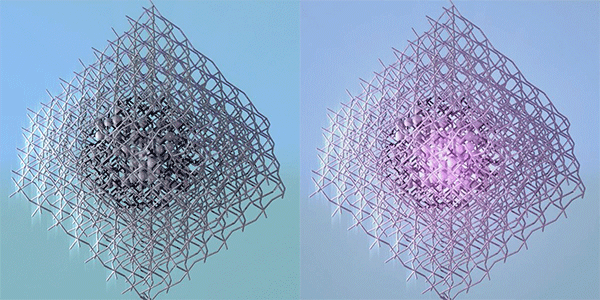
University of Toronto researchers combine 2 different materials for new hyper-efficient, light-emitting, hybrid crystal

The Sargent Group at the University of Toronto has been quite active with regard to LEDs (light-emitting diodes) and with quantum dots. Their latest work is announced in a July 16, 2015 news item on Nanotechnology Now (Note: I had to include the ‘oatmeal cookie and chocolate chips’ analogy in the first paragraph as it’s referred to subsequently),

It’s snack time: you have a plain oatmeal cookie, and a pile of chocolate chips. Both are delicious on their own, but if you can find a way to combine them smoothly, you get the best of both worlds.

Researchers in The Edward S. Rogers Sr. Department of Electrical & Computer Engineering [University of Toronto] used this insight to invent something totally new: they’ve combined two promising solar cell materials together for the first time, creating a new platform for LED technology.

The team designed a way to embed strongly luminescent nanoparticles called colloidal quantum dots (the chocolate chips) into perovskite (the oatmeal cookie). Perovskites are a family of materials that can be easily manufactured from solution, and that allow electrons to move swiftly through them with minimal loss or capture by defects.

A July 15, 2015 University of Toronto news release (also on EurekAlert), which originated the news item, reveals more about the research (Note: A link has been removed),

“It’s a pretty novel idea to blend together these two optoelectronic materials, both of which are gaining a lot of traction,” says Xiwen Gong, one of the study’s lead authors and a PhD candidate working with Professor Ted Sargent. “We wanted to take advantage of the benefits of both by combining them seamlessly in a solid-state matrix.”

The result is a black crystal that relies on the perovskite matrix to ‘funnel’ electrons into the quantum dots, which are extremely efficient at converting electricity to light. Hyper-efficient LED technologies could enable applications from the visible-light LED bulbs in every home, to new displays, to gesture recognition using near-infrared wavelengths.

“When you try to jam two different crystals together, they often form separate phases without blending smoothly into each other,” says Dr. Riccardo Comin, a post-doctoral fellow in the Sargent Group. “We had to design a new strategy to convince these two components to forget about their differences and to rather intermix into forming a unique crystalline entity.”

The main challenge was making the orientation of the two crystal structures line up, called heteroexpitaxy. To achieve heteroepitaxy, Gong, Comin and their team engineered a way to connect the atomic ‘ends’ of the two crystalline structures so that they aligned smoothly, without defects forming at the seams. “We started by building a nano-scale scaffolding ‘shell’ around the quantum dots in solution, then grew the perovskite crystal around that shell so the two faces aligned,” explained coauthor Dr. Zhijun Ning, who contributed to the work while a post-doctoral fellow at UofT and is now a faculty member at ShanghaiTech.

The resulting heterogeneous material is the basis for a new family of highly energy-efficient near-infrared LEDs. Infrared LEDs can be harnessed for improved night-vision technology, to better biomedical imaging, to high-speed telecommunications.

Combining the two materials in this way also solves the problem of self-absorption, which occurs when a substance partly re-absorbs the same spectrum of energy that it emits, with a net efficiency loss. “These dots in perovskite don’t suffer reabsorption, because the emission of the dots doesn’t overlap with the absorption spectrum of the perovskite,” explains Comin.

Gong, Comin and the team deliberately designed their material to be compatible with solution-processing, so it could be readily integrated with the most inexpensive and commercially practical ways of manufacturing solar film and devices. Their next step is to build and test the hardware to capitalize on the concept they have proven with this work.

“We’re going to build the LED device and try to beat the record power efficiency reported in the literature,” says Gong.

I see that Sargent’s work is still associated with and supported by Saudi Arabia, from the news release,

This work was supported by the Ontario Research Fund Research Excellence Program, the Natural Sciences and Engineering Research Council of Canada (NSERC), and the King Abdullah University of Science & Technology (KAUST).

Here’s a link to and a citation for the paper,

Quantum-dot-in-perovskite solids by Zhijun Ning, Xiwen Gong, Riccardo Comin, Grant Walters, Fengjia Fan, Oleksandr Voznyy, Emre Yassitepe, Andrei Buin, Sjoerd Hoogland, & Edward H. Sargent. Nature 523, 324–328 (16 July 2015) doi:10.1038/nature14563 Published online 15 July 2015

This paper is behind a paywall.

Finally, the researchers have made a .gif of their hybrid crystal available.

A glowing quantum dot seamlessly integrated into a perovskite crystal matrix (Image: Ella Marushchenko). Courtesy: University of Toronto

A glowing quantum dot seamlessly integrated into a perovskite crystal matrix (Image: Ella Marushchenko). Courtesy: University of Toronto

ETA July 17, 2015:

Dexter Johnson provides some additional insight into the work in his July 16, 2015 posting on the Nanoclast blog (on the Institute for Electrical and Electronics Engineers website), Note:  Links have been removed,

Ted Sargent at the University of Toronto has built a reputation over the years as being a prominent advocate for the use of quantum dots in photovoltaics. Sargent has even penned a piece for IEEE Spectrum covering the topic, and this blog has covered his record breaking efforts at boosting the conversion efficiency of quantum dot-based photovoltaics a few times.

Earlier this year, however, Sargent started to take an interest in the hot material that has the photovoltaics community buzzing: perovskite. …