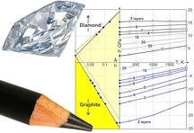
The ‘scotch-tape’ technique is mythologized in the graphene origins story which has scientists, Andre Geim and Konstantin Novoselov, first isolating the material by using adhesive (aka ‘sticky’ tape or ‘scotch’ tape) as per my Oct. 7, 2010 posting,
The technique that Geim and Novoselov used to create the first graphene sheets both amuses and fascinates me (from the article by Kit Eaton on the Fast Company website),
The two scientists came up with the technique that first resulted in samples of graphene–peeling individual atoms-deep sheets of the material from a bigger block of pure graphite. The science here seems almost foolishly simple, but it took a lot of lateral thinking to dream up, and then some serious science to investigate: Geim and Novoselo literally “ripped” single sheets off the graphite by using regular adhesive tape. Once they’d confirmed they had grabbed micro-flakes of the material, Geim and Novoselo were responsible for some of the very early experiments into the material’s properties. Novel stuff indeed, but perhaps not so unexpected from a scientist (Geim) who the Nobel Committe notes once managed to make a frog levitate in a magnetic field.
A May 21, 2014 article about Geim who has won both a Nobel and an Ig Nobel (the only scientist to do so) and graphene by Sarah Lewis for Fast Company offers more details about the discovery,
The graphene FNE [Friday Night Experiments] began when Geim asked Da Jiang, a doctoral student from China, to polish a piece of graphite an inch across and a few millimeters thick down to 10 microns using a specialized machine. Partly due to a language barrier, Jiang polished the graphite down to dust, but not the ultimate thinness Geim wanted.
Helpfully, the Geim lab was also observing graphite using scanning tunneling microscopy (STM). The experimenters would clean the samples beforehand using Scotch tape, which they would then discard. “We took it out of the trash and just used it,” Novoselov said. The flakes of graphite on the tape from the waste bin were finer and thinner than what Jiang had found using the fancy machine. They weren’t one layer thick—that achievement came by ripping them some more with Scotch tape.
They swapped the adhesive for Japanese Nitto tape, “probably because the whole process is so simple and cheap we wanted to fancy it up a little and use this blue tape,” Geim said. Yet “the method is called the ‘Scotch tape technique.’ I fought against this name, but lost.”
Scientists elsewhere have been inspired to investigate the process in minute detail as per a June 27, 2014 news item on Nanowerk,
The simplest mechanical cleavage technique using a primitive “Scotch” tape has resulted in the Nobel-awarded discovery of graphenes and is currently under worldwide use for assembling graphenes and other two-dimensional (2D) graphene-like structures toward their utilization in novel high-performance nanoelectronic devices.
The simplicity of this method has initiated a booming research on 2D materials. However, the atomistic processes behind the micromechanical cleavage have still been poorly understood.
A June 27, 2014 MANA (International Center for Materials Nanoarchitectoinics) news release, which originated the news item, provides more information,
A joined team of experimentalists and theorists from the International Center for Young Scientists, International Center for Materials Nanoarchitectonics and Surface Physics and Structure Unit of the National Institute for Materials Science, National University of Science and Technology “MISiS” (Moscow, Russia), Rice University (USA) and University of Jyväskylä (Finland) led by Daiming Tang and Dmitri Golberg for the first time succeeded in complete understanding of physics, kinetics and energetics behind the regarded “Scotch-tape” technique using molybdenum disulphide (MoS2) atomic layers as a model material.
The researchers developed a direct in situ probing technique in a high-resolution transmission electron microscope (HRTEM) to investigate the mechanical cleavage processes and associated mechanical behaviors. By precisely manipulating an ultra-sharp metal probe to contact the pre-existing crystalline steps of the MoS2 single crystals, atomically thin flakes were delicately peeled off, selectively ranging from a single, double to more than 20 atomic layers. The team found that the mechanical behaviors are strongly dependent on the number of layers. Combination of in situ HRTEM and molecular dynamics simulations reveal a transformation of bending behavior from spontaneous rippling (< 5 atomic layers) to homogeneous curving (~ 10 layers), and finally to kinking (20 or more layers).
By considering the force balance near the contact point, the specific surface energy of a MoS2 monoatomic layer was calculated to be ~0.11 N/m. This is the first time that this fundamentally important property has directly been measured.
After initial isolation from the mother crystal, the MoS2 monolayer could be readily restacked onto the surface of the crystal, demonstrating the possibility of van der Waals epitaxy. MoS2 atomic layers could be bent to ultimate small radii (1.3 ~ 3.0 nm) reversibly without fracture. Such ultra-reversibility and extreme flexibility proves that they could be mechanically robust candidates for the advanced flexible electronic devices even under extreme folding conditions.
Here’s a link to and a citation for the research paper,
Nanomechanical cleavage of molybdenum disulphide atomic layers by Dai-Ming Tang, Dmitry G. Kvashnin, Sina Najmaei, Yoshio Bando, Koji Kimoto, Pekka Koskinen, Pulickel M. Ajayan, Boris I. Yakobson, Pavel B. Sorokin, Jun Lou, & Dmitri Golberg. Nature Communications 5, Article number: 3631 doi:10.1038/ncomms4631 Published 03 April 2014
This paper is behind a paywall but there is a free preview available through ReadCube Access.
