Tag Archives: perovskite

Artificial intelligence (AI) consumes a lot of energy but tree-like memory may help conserve it

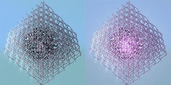
A simulation of a quantum material’s properties reveals its ability to learn numbers, a test of artificial intelligence. (Purdue University image/Shakti Wadekar)

A May 7, 2020 Purdue University news release (also on EurekAlert) describes a new approach for energy-efficient hardware in support of artificial intelligence (AI) systems,

To just solve a puzzle or play a game, artificial intelligence can require software running on thousands of computers. That could be the energy that three nuclear plants produce in one hour.

A team of engineers has created hardware that can learn skills using a type of AI that currently runs on software platforms. Sharing intelligence features between hardware and software would offset the energy needed for using AI in more advanced applications such as self-driving cars or discovering drugs.

“Software is taking on most of the challenges in AI. If you could incorporate intelligence into the circuit components in addition to what is happening in software, you could do things that simply cannot be done today,” said Shriram Ramanathan, a professor of materials engineering at Purdue University.

AI hardware development is still in early research stages. Researchers have demonstrated AI in pieces of potential hardware, but haven’t yet addressed AI’s large energy demand.

As AI penetrates more of daily life, a heavy reliance on software with massive energy needs is not sustainable, Ramanathan said. If hardware and software could share intelligence features, an area of silicon might be able to achieve more with a given input of energy.

Ramanathan’s team is the first to demonstrate artificial “tree-like” memory in a piece of potential hardware at room temperature. Researchers in the past have only been able to observe this kind of memory in hardware at temperatures that are too low for electronic devices.

The results of this study are published in the journal Nature Communications.

The hardware that Ramanathan’s team developed is made of a so-called quantum material. These materials are known for having properties that cannot be explained by classical physics. Ramanathan’s lab has been working to better understand these materials and how they might be used to solve problems in electronics.

Software uses tree-like memory to organize information into various “branches,” making that information easier to retrieve when learning new skills or tasks.

The strategy is inspired by how the human brain categorizes information and makes decisions.

“Humans memorize things in a tree structure of categories. We memorize ‘apple’ under the category of ‘fruit’ and ‘elephant’ under the category of ‘animal,’ for example,” said Hai-Tian Zhang, a Lillian Gilbreth postdoctoral fellow in Purdue’s College of Engineering. “Mimicking these features in hardware is potentially interesting for brain-inspired computing.”

The team introduced a proton to a quantum material called neodymium nickel oxide. They discovered that applying an electric pulse to the material moves around the proton. Each new position of the proton creates a different resistance state, which creates an information storage site called a memory state. Multiple electric pulses create a branch made up of memory states.

“We can build up many thousands of memory states in the material by taking advantage of quantum mechanical effects. The material stays the same. We are simply shuffling around protons,” Ramanathan said.

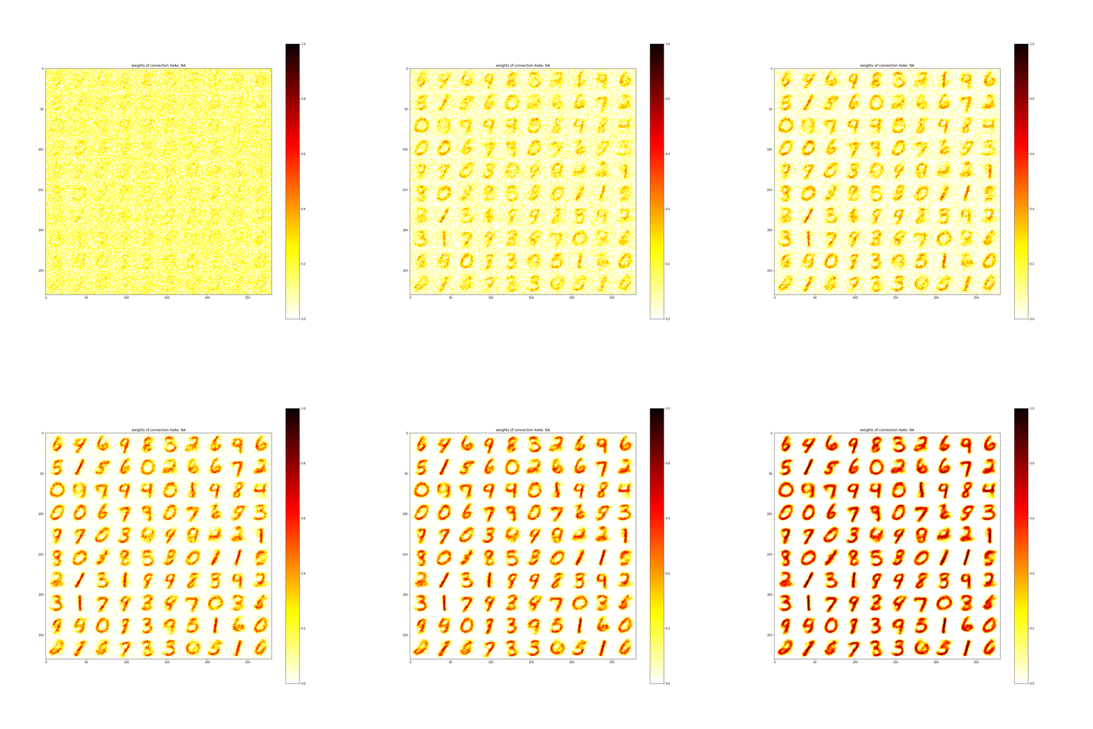
Through simulations of the properties discovered in this material, the team showed that the material is capable of learning the numbers 0 through 9. The ability to learn numbers is a baseline test of artificial intelligence.

The demonstration of these trees at room temperature in a material is a step toward showing that hardware could offload tasks from software.

“This discovery opens up new frontiers for AI that have been largely ignored because implementing this kind of intelligence into electronic hardware didn’t exist,” Ramanathan said.

The material might also help create a way for humans to more naturally communicate with AI.

“Protons also are natural information transporters in human beings. A device enabled by proton transport may be a key component for eventually achieving direct communication with organisms, such as through a brain implant,” Zhang said.

Here’s a link to and a citation for the published study,

Perovskite neural trees by Hai-Tian Zhang, Tae Joon Park, Shriram Ramanathan. Nature Communications volume 11, Article number: 2245 (2020) DOI: https://doi.org/10.1038/s41467-020-16105-y Published: 07 May 2020

This paper is open access.
Making perovskite solar cells more stable and more humidity tolerant

Living in what’s considered a humid environment the news of solar cells that are humidity-resistant caught my attention. From a July 18, 2016 news item on phys.org,

Widely known as one of the cleanest and most renewable energy sources, solar energy is a fast growing alternative to fossil fuels. Among the various types of solar materials, organometal halide perovskite in particular has attracted researchers’ attention thanks to its superior optical and electronic properties. With a dramatic increase in the power conversion efficiency (PCE) from 3% in 2009 to as high as over 22% today [according to my July 13, 2016 posting that efficiency could now be as high as 31%], perovskite solar cells are considered as a promising next-generation energy device; only except that perovskite is weak to water and quickly loses its stability and performance in a damp, humid environment.

A team of Korean researchers led by Taiho Park at Pohang University of Science and Technology (POSTECH), Korea, has found a new method to improve not only the efficiency, but stability and humidity tolerance of perovskite solar cells. Park and his students, Guan-Woo Kim and Gyeongho Kang, designed a hydrophobic conducting polymer that has high hole mobility without the need of additives, which tend to easily absorb moisture in the air. …

A July 18, 2016 Pohang University of Science and Technology (POSTECH) press release on EurekAlert, which originated the news item, provides more information about the work,

Perovskite solar cells in general consist of a transparent electrode, an electron transport layer, perovskite, a hole transport layer, and a metal electrode. The hole transport layer is important because it not only transports holes to the electrode but also prevents perovskite from being directly exposed to air. Spiro-MeOTAD, a conventionally used hole-transport material, needs additives due to its intrinsically low hole mobility. However, Bis(trifluoromethane)sulfonimide lithium salt (LiTFSI), one of the common additives, is prone to suck in moisture in the air. Moreover, Spiro-MeOTAD forms a slightly hydrophilic layer that easily dissolves in water, and thus it cannot work as a moisture barrier itself.

Park’s team focused on an idea of an additive-free (dopant-free) polymeric hole transport layer. They designed and synthesized a hydrophobic conducting polymer by combining benzodithiophene (BDT) and benzothiadiazole (BT). As the new polymer has a face-on orientation, which helps vertical charge transport of holes, the researchers were able to achieve high hole mobility without any additives.

Park and colleagues confirmed that the perovskite solar cells with the new polymer showed high efficiency of 17.3% and dramatically improved stability — the cells retained the high efficiency for over 1400 hours, almost two months, under 75 percent humidity.

“We believe that our findings will bring perovskite one step closer to use and accelerate the commercialization of perovskite solar cells,” commented Taiho Park, a professor with the Department of Chemical Engineering at POSTECH.

Here’s a link to and a citation for the paper,

Dopant-free polymeric hole transport materials for highly efficient and stable perovskite solar cells by Guan-Woo Kim, Gyeongho Kang, Jinseck Kim, Gang-Young Lee, Hong Il Kim, Limok Pyeon, Jaechol Lee, and Taiho Park. Energy Environ. Sci., 2016,9, 2326-2333 DOI: 10.1039/C6EE00709K First published online 28 Apr 2016

I wonder if the press release was originally written in April 2016? That would explain the difference in efficiency I noted earlier in the press release. Getting back to the paper, it is open access with three different means of accessing the material from the publisher, the Royal Society of Chemistry.

Pushing efficiency of perovskite-based solar cells to 31%

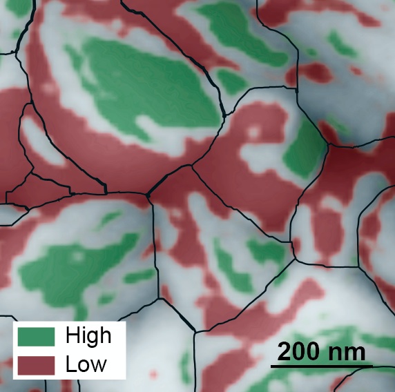
This atomic force microscopy image of the grainy surface of a perovskite solar cell reveals a new path to much greater efficiency. Individual grains are outlined in black, low-performing facets are red, and high-performing facets are green. A big jump in efficiency could possibly be obtained if the material can be grown so that more high-performing facets develop. (Credit: Berkeley Lab)

This atomic force microscopy image of the grainy surface of a perovskite solar cell reveals a new path to much greater efficiency. Individual grains are outlined in black, low-performing facets are red, and high-performing facets are green. A big jump in efficiency could possibly be obtained if the material can be grown so that more high-performing facets develop. (Credit: Berkeley Lab)

It’s always fascinating to observe a trend (or a craze) in science, an endeavour that outsiders (like me) tend to think of as impervious to such vagaries. Perovskite seems to be making its way past the trend/craze phase and moving into a more meaningful phase. From a July 4, 2016 news item on Nanowerk,

Scientists from the Department of Energy’s Lawrence Berkeley National Laboratory (Berkeley Lab) have discovered a possible secret to dramatically boosting the efficiency of perovskite solar cells hidden in the nanoscale peaks and valleys of the crystalline material.

Solar cells made from compounds that have the crystal structure of the mineral perovskite have captured scientists’ imaginations. They’re inexpensive and easy to fabricate, like organic solar cells. Even more intriguing, the efficiency at which perovskite solar cells convert photons to electricity has increased more rapidly than any other material to date, starting at three percent in 2009 — when researchers first began exploring the material’s photovoltaic capabilities — to 22 percent today. This is in the ballpark of the efficiency of silicon solar cells.

Now, as reported online July 4, 2016 in the journal Nature Energy (“Facet-dependent photovoltaic efficiency variations in single grains of hybrid halide perovskite”), a team of scientists from the Molecular Foundry and the Joint Center for Artificial Photosynthesis, both at Berkeley Lab, found a surprising characteristic of a perovskite solar cell that could be exploited for even higher efficiencies, possibly up to 31 percent.

A July 4, 2016 Berkeley Lab news release (also on EurekAlert), which originated the news item, details the research,

Using photoconductive atomic force microscopy, the scientists mapped two properties on the active layer of the solar cell that relate to its photovoltaic efficiency. The maps revealed a bumpy surface composed of grains about 200 nanometers in length, and each grain has multi-angled facets like the faces of a gemstone.

Unexpectedly, the scientists discovered a huge difference in energy conversion efficiency between facets on individual grains. They found poorly performing facets adjacent to highly efficient facets, with some facets approaching the material’s theoretical energy conversion limit of 31 percent.

The scientists say these top-performing facets could hold the secret to highly efficient solar cells, although more research is needed.

“If the material can be synthesized so that only very efficient facets develop, then we could see a big jump in the efficiency of perovskite solar cells, possibly approaching 31 percent,” says Sibel Leblebici, a postdoctoral researcher at the Molecular Foundry.

Leblebici works in the lab of Alexander Weber-Bargioni, who is a corresponding author of the paper that describes this research. Ian Sharp, also a corresponding author, is a Berkeley Lab scientist at the Joint Center for Artificial Photosynthesis. Other Berkeley Lab scientists who contributed include Linn Leppert, Francesca Toma, and Jeff Neaton, the director of the Molecular Foundry.

A team effort

The research started when Leblebici was searching for a new project. “I thought perovskites are the most exciting thing in solar right now, and I really wanted to see how they work at the nanoscale, which has not been widely studied,” she says.

She didn’t have to go far to find the material. For the past two years, scientists at the nearby Joint Center for Artificial Photosynthesis have been making thin films of perovskite-based compounds, and studying their ability to convert sunlight and CO2 into useful chemicals such as fuel. Switching gears, they created pervoskite solar cells composed of methylammonium lead iodide. They also analyzed the cells’ performance at the macroscale.

The scientists also made a second set of half cells that didn’t have an electrode layer. They packed eight of these cells on a thin film measuring one square centimeter. These films were analyzed at the Molecular Foundry, where researchers mapped the cells’ surface topography at a resolution of ten nanometers. They also mapped two properties that relate to the cells’ photovoltaic efficiency: photocurrent generation and open circuit voltage.

This was performed using a state-of-the-art atomic force microscopy technique, developed in collaboration with Park Systems, which utilizes a conductive tip to scan the material’s surface. The method also eliminates friction between the tip and the sample. This is important because the material is so rough and soft that friction can damage the tip and sample, and cause artifacts in the photocurrent.

Surprise discovery could lead to better solar cells

The resulting maps revealed an order of magnitude difference in photocurrent generation, and a 0.6-volt difference in open circuit voltage, between facets on the same grain. In addition, facets with high photocurrent generation had high open circuit voltage, and facets with low photocurrent generation had low open circuit voltage.

“This was a big surprise. It shows, for the first time, that perovskite solar cells exhibit facet-dependent photovoltaic efficiency,” says Weber-Bargioni.

Adds Toma, “These results open the door to exploring new ways to control the development of the material’s facets to dramatically increase efficiency.”

In practice, the facets behave like billions of tiny solar cells, all connected in parallel. As the scientists discovered, some cells operate extremely well and others very poorly. In this scenario, the current flows towards the bad cells, lowering the overall performance of the material. But if the material can be optimized so that only highly efficient facets interface with the electrode, the losses incurred by the poor facets would be eliminated.

“This means, at the macroscale, the material could possibly approach its theoretical energy conversion limit of 31 percent,” says Sharp.

A theoretical model that describes the experimental results predicts these facets should also impact the emission of light when used as an LED. …

The Molecular Foundry is a DOE Office of Science User Facility located at Berkeley Lab. The Joint Center for Artificial Photosynthesis is a DOE Energy Innovation Hub led by the California Institute of Technology in partnership with Berkeley Lab.

Here’s a link to and a citation for the paper,

Facet-dependent photovoltaic efficiency variations in single grains of hybrid halide perovskite by Sibel Y. Leblebici, Linn Leppert, Yanbo Li, Sebastian E. Reyes-Lillo, Sebastian Wickenburg, Ed Wong, Jiye Lee, Mauro Melli, Dominik Ziegler, Daniel K. Angell, D. Frank Ogletree, Paul D. Ashby, Francesca M. Toma, Jeffrey B. Neaton, Ian D. Sharp, & Alexander Weber-Bargioni. Nature Energy 1, Article number: 16093 (2016  doi:10.1038/nenergy.2016.93 Published online: 04 July 2016

This paper is behind a paywall.

Dexter Johnson’s July 6, 2016 posting on his Nanoclast blog (on the IEEE [Institute of Electrical and Electronics Engineers] website} presents his take on the impact that this new finding may have,

The rise of the crystal perovskite as a potential replacement for silicon in photovoltaics has been impressive over the last decade, with its conversion efficiency improving from 3.8 to 22.1 percent over that time period. Nonetheless, there has been a vague sense that this rise is beginning to peter out of late, largely because when a solar cell made from perovskite gets larger than 1 square centimeter the best conversion efficiency had been around 15.6 percent. …

Back to the mortar and pestle for perovskite-based photovoltaics

This mechanochemistry (think mortar and pestle) story about perovskite comes from Poland. From a Jan. 14, 2016 Institute of Physical Chemistry of the Polish Academy of Sciences press release (also on EurekAlert but dated Jan. 16, 2016),

Perovskites, substances that perfectly absorb light, are the future of solar energy. The opportunity for their rapid dissemination has just increased thanks to a cheap and environmentally safe method of production of these materials, developed by chemists from Warsaw, Poland. Rather than in solutions at a high temperature, perovskites can now be synthesized by solid-state mechanochemical processes: by grinding powders.

We associate the milling of chemicals less often with progress than with old-fashioned pharmacies and their inherent attributes: the pestle and mortar. [emphasis mine] It’s time to change this! Recent research findings show that by the use of mechanical force, effective chemical transformations take place in solid state. Mechanochemical reactions have been under investigation for many years by the teams of Prof. Janusz Lewinski from the Institute of Physical Chemistry of the Polish Academy of Sciences (IPC PAS) and the Faculty of Chemistry of Warsaw University of Technology. In their latest publication, the Warsaw researchers describe a surprisingly simple and effective method of obtaining perovskites – futuristic photovoltaic materials with a spatially complex crystal structure.

“With the aid of mechanochemistry we are able to synthesize a variety of hybrid inorganic-organic functional materials with a potentially great significance for the energy sector. Our youngest ‘offspring’ are high quality perovskites. These compounds can be used to produce thin light-sensitive layers for high efficiency solar cells,” says Prof. Lewinski.

Perovskites are a large group of materials, characterized by a defined spatial crystalline structure. In nature, the perovskite naturally occurring as a mineral is calcium titanium(IV) oxide CaTiO3. Here the calcium atoms are arranged in the corners of the cube, in the middle of each wall there is an oxygen atom and at the centre of the cube lies a titanium atom. In other types of perovskite the same crystalline structure can be constructed of various organic and inorganic compounds, which means titanium can be replaced by, for example, lead, tin or germanium. As a result, the properties of the perovskite can be adjusted so as to best fit the specific application, for example, in photovoltaics or catalysis, but also in the construction of superconducting electromagnets, high voltage transformers, magnetic refrigerators, magnetic field sensors, or RAM memories.

At first glance, the method of production of perovskites using mechanical force, developed at the IPC PAS, looks a little like magic.

“Two powders are poured into the ball mill: a white one, methylammonium iodide CH3NH3I, and a yellow one, lead iodide PbI2. After several minutes of milling no trace is left of the substrates. Inside the mill there is only a homogeneous black powder: the perovskite CH3NH3PbI3,” explains doctoral student Anna Maria Cieslak (IPC PAS).

“Hour after hour of waiting for the reaction product? Solvents? High temperatures? In our method, all this turns out to be unnecessary! We produce chemical compounds by reactions occurring only in solids at room temperature,” stresses Dr. Daniel Prochowicz (IPC PAS).

The mechanochemically manufactured perovskites were sent to the team of Prof. Michael Graetzel from the Ecole Polytechnique de Lausanne in Switzerland, where they were used to build a new laboratory solar cell. The performance of the cell containing the perovskite with a mechanochemical pedigree proved to be more than 10% greater than a cell’s performance with the same construction, but containing an analogous perovskite obtained by the traditional method, involving solvents.

“The mechanochemical method of synthesis of perovskites is the most environmentally friendly method of producing this class of materials. Simple, efficient and fast, it is ideal for industrial applications. With full responsibility we can state: perovskites are the materials of the future, and mechanochemistry is the future of perovskites,” concludes Prof. Lewinski.

The described research will be developed within GOTSolar collaborative project funded by the European Commission under the Horizon 2020 Future and Emerging Technologies action.

Perovskites are not the only group of three-dimensional materials that has been produced mechanochemically by Prof. Lewinski’s team. In a recent publication the Warsaw researchers showed that by using the milling technique they can also synthesize inorganic-organic microporous MOF (Metal-Organic Framework) materials. The free space inside these materials is the perfect place to store different chemicals, including hydrogen.

This research was published back in August 2015,

Mechanosynthesis of the hybrid perovskite CH3NH3PbI3: characterization and the corresponding solar cell efficiency by D. Prochowicz, M. Franckevičius, A. M. Cieślak, S. M. Zakeeruddin, M. Grätzel and J. Lewiński. J. Mater. Chem. A, 2015,3, 20772-20777 DOI: 10.1039/C5TA04904K First published online 27 Aug 2015

This paper is behind a paywall.

A perovskite memristor with three stable resistive states

Thanks to Dexter Johnson’s Oct. 22, 2015 posting on his Nanoclast blog (on the IEEE [Institute of Electrical and Electronics Engineers]) website, I’ve found information about a second memristor with three terminals, aka, three stable resistive states,  (the first is mentioned in my April 10, 2015 posting). From Dexter’s posting (Note: Links have been removed),

Now researchers at ETH Zurich have designed a memristor device out of perovskite just 5 nanometres thick that has three stable resistive states, which means it can encode data as 0,1 and 2, or a “trit” as opposed to a “bit.”

The research, which was published in the journal ACS Nano, developed model devices that have two competing nonvolatile resistive switching processes. These switching processes can be alternatively triggered by the effective switching voltage and time applied to the device.

“Our component could therefore also be useful for a new type of IT (Information Technology) that is not based on binary logic, but on a logic that provides for information located ‘between’ the 0 and 1,” said Jennifer Rupp, professor in the Department of Materials at ETH Zurich, in a press release. “This has interesting implications for what is referred to as fuzzy logic, which seeks to incorporate a form of uncertainty into the processing of digital information. You could describe it as less rigid computing.”

An Oct. 19, 2015 Swiss National Science Foundation press release provides context for the research,

Two IT giants, Intel and HP, have entered a race to produce a commercial version of memristors, a new electronics component that could one day replace flash memory (DRAM) used in USB memory sticks, SD cards and SSD hard drives. “Basically, memristors require less energy since they work at lower voltages,” explains Jennifer Rupp, professor in the Department of Materials at ETH Zurich and holder of a SNSF professorship grant. “They can be made much smaller than today’s memory modules, and therefore offer much greater density. This means they can store more megabytes of information per square millimetre.” But currently memristors are only at the prototype stage. [emphasis mine]

There is a memristor-based product on the market as I noted in a Sept. 10, 2015 posting, although that may not be the type of memristive device that Rupp seems to be discussing. (Should you have problems accessing the Swiss National Science Foundation press release, you can find a lightly edited version (a brief [two sentences] history of the memristor has been left out) here on Azonano.

Jacopo Prisco wrote for CNN online in a March 2, 2015 article about memristors and Rupp’s work (Note: A link has been removed),

Simply put, the memristor could mean the end of electronics as we know it and the beginning of a new era called “ionics”.

The transistor, developed in 1947, is the main component of computer chips. It functions using a flow of electrons, whereas the memristor couples the electrons with ions, or electrically charged atoms.

In a transistor, once the flow of electrons is interrupted by, say, cutting the power, all information is lost. But a memristor can remember the amount of charge that was flowing through it, and much like a memory stick it will retain the data even when the power is turned off.

This can pave the way for computers that will instantly turn on and off like a light bulb and never lose data: the RAM, or memory, will no longer be erased when the machine is turned off, without the need to save anything to hard drives as with current technology.

Jennifer Rupp is a Professor of electrochemical materials at ETH Zurich, and she’s working with IBM to build a memristor-based machine.

Memristors, she points out, function in a way that is similar to a human brain: “Unlike a transistor, which is based on binary codes, a memristor can have multi-levels. You could have several states, let’s say zero, one half, one quarter, one third, and so on, and that gives us a very powerful new perspective on how our computers may develop in the future,” she told CNN’s Nick Glass.

This is the CNN interview with Rupp,

Prisco also provides an update about HP’s memristor-based product,

After manufacturing the first ever memristor, Hewlett Packard has been working for years on a new type of computer based on the technology. According to plans, it will launch by 2020.

Simply called “The Machine”, it uses “electrons for processing, photons for communication, and ions for storage.”

I first wrote about HP’s The Machine in a June 25, 2014 posting (scroll down about 40% of the way).

There are many academic teams researching memristors including a team at Northwestern University. I highlighted their announcement of a three-terminal version in an April 10, 2015 posting. While Rupp’s team achieved its effect with a perovskite substrate, the Northwestern team used a molybdenum disulfide (MoS2) substrate.

For anyone wanting to read the latest research from ETH, here’s a link to and a citation for the paper,

Uncovering Two Competing Switching Mechanisms for Epitaxial and Ultrathin Strontium Titanate-Based Resistive Switching Bits by Markus Kubicek, Rafael Schmitt, Felix Messerschmitt, and Jennifer L. M. Rupp. ACS Nano, Article ASAP DOI: 10.1021/acsnano.5b02752 Publication Date (Web): October 8, 2015

Copyright © 2015 American Chemical Society

This paper is behind a paywall.

Finally, should you find the commercialization aspects of the memristor story interesting, there’s a June 6, 2015 posting by Knowm CEO (chief executive officer) Alex Nugent waxes eloquent on HP Labs’ ‘memristor problem’ (Note: A link has been removed),

Today I read something that did not surprise me. HP has said that their memristor technology will be replaced by traditional DRAM memory for use in “The Machine”. This is not surprising for those of us who have been in the field since before HP’s memristor marketing engine first revved up in 2008. While I have to admit the miscommunication between HP’s research and business development departments is starting to get really old, I do understand the problem, or at least part of it.

There are two ways to develop memristors. The first way is to force them to behave as you want them to behave. Most memristors that I have seen do not behave like fast, binary, non-volatile, deterministic switches. This is a problem because this is how HP wants them to behave. Consequently a perception has been created that memristors are for non-volatile fast memory. HP wants a drop-in replacement for standard memory because this is a large and established market. Makes sense of course, but its not the whole story on memristors.

Memristors exhibit a huge range of amazing phenomena. Some are very fast to switch but operate probabilistically. Others can be changed a little bit at a time and are ideal for learning. Still others have capacitance (with memory), or act as batteries. I’ve even seen some devices that can be programmed to be a capacitor or a resistor or a memristor. (Seriously).

Nugent, whether you agree with him or not provides, some fascinating insight. In the excerpt I’ve included here, he seems to provide confirmation that it’s possible to state ‘there are no memristors on the market’ and ‘there are memristors on the market’ because different devices are being called memristors.

Perovskite, nanorods, and solar energy

As the authors, Azhar Fakharuddin, Rajan Jose, and Thomas Brown, note in an Aug. 7, 2015 Nanowerk Spotlight article , securing energy sources is a global pursuit and pervoskite (a new wonder material for solar cells) has presented a challenge (Note: A link has been removed),

Energy security has been a top global concern motivating researchers to seek it from renewable and cost-effective resources. Solar cells, that convert sun light into electricity, hold the promise as a cheap energy alternative. The silicon and thin film photovoltaic industry have taken many strides to lower energy prices; however, continued research is required in order to extensively compete with fossil fuels.

The development of perovskite solar cells, first reported in 2009 (and with a record power conversion efficiency of 20.1 percent so far), is a possible route towards high efficiency photovoltaics that are also cost-effectiveness, owing to to their easy-processing from solution.

Question marks have however remained on their stability.

The authors (members of a research team) have recently published a paper about a method that could make perovskite solar cells more stable,

Now, a research team from University Malaysia Pahang, focussing on renewable energy, working in in collaboration with scientists from University of Rome ‘Tor Vergata’, Italy, has developed the world’s first nanorod-based perovskite solar module.

Among the three types of electron transport layers investigated, the nanorod-based devices retained the original efficiency values even after 2500 hours of shelf-life investigation, a protocol used to gauge initial stability and indoor lifetime performance.
The device employing a conventional TiO2 nanoparticle material showed nearly 60% of original performance, whereas planar devices employing a compact TiO2 layer showed below 5% of original performance, measured at similar experimental conditions.
A chemical analysis of the devices hinted that the peculiar conformation of nanorods facilitates a stable perovskite phase due to their inherent stability and macroporous nature.

If you want more detail, the research team’s Nanowerk Spotlight article is the place to look (it’s almost like a Reddit session except there’s no ‘ask me anything’ option). There’s also the team’s paper,

Vertical TiO2 Nanorods as a Medium for Stable and High-Efficiency Perovskite Solar Modules by Azhar Fakharuddin, Francesco Di Giacomo, Alessandro L. Palma, Fabio Matteocci, Irfan Ahmed, Stefano Razza, Alessandra D’Epifanio, Silvia Licoccia, Jamil Ismail, Aldo Di Carlo, Thomas M. Brown, and Rajan Jose. ACS Nano, Article ASAP DOI: 10.1021/acsnano.5b03265 Publication Date (Web): July 24, 2015

Copyright © 2015 American Chemical Society

This paper is behind a paywall.

One final note, I’ve been meaning to publish a post about perovskite-based solar cells for a while now as the material seems to be sweeping the solar energy community and, now, it’s done.

University of Toronto researchers combine 2 different materials for new hyper-efficient, light-emitting, hybrid crystal

The Sargent Group at the University of Toronto has been quite active with regard to LEDs (light-emitting diodes) and with quantum dots. Their latest work is announced in a July 16, 2015 news item on Nanotechnology Now (Note: I had to include the ‘oatmeal cookie and chocolate chips’ analogy in the first paragraph as it’s referred to subsequently),

It’s snack time: you have a plain oatmeal cookie, and a pile of chocolate chips. Both are delicious on their own, but if you can find a way to combine them smoothly, you get the best of both worlds.

Researchers in The Edward S. Rogers Sr. Department of Electrical & Computer Engineering [University of Toronto] used this insight to invent something totally new: they’ve combined two promising solar cell materials together for the first time, creating a new platform for LED technology.

The team designed a way to embed strongly luminescent nanoparticles called colloidal quantum dots (the chocolate chips) into perovskite (the oatmeal cookie). Perovskites are a family of materials that can be easily manufactured from solution, and that allow electrons to move swiftly through them with minimal loss or capture by defects.

A July 15, 2015 University of Toronto news release (also on EurekAlert), which originated the news item, reveals more about the research (Note: A link has been removed),

“It’s a pretty novel idea to blend together these two optoelectronic materials, both of which are gaining a lot of traction,” says Xiwen Gong, one of the study’s lead authors and a PhD candidate working with Professor Ted Sargent. “We wanted to take advantage of the benefits of both by combining them seamlessly in a solid-state matrix.”

The result is a black crystal that relies on the perovskite matrix to ‘funnel’ electrons into the quantum dots, which are extremely efficient at converting electricity to light. Hyper-efficient LED technologies could enable applications from the visible-light LED bulbs in every home, to new displays, to gesture recognition using near-infrared wavelengths.

“When you try to jam two different crystals together, they often form separate phases without blending smoothly into each other,” says Dr. Riccardo Comin, a post-doctoral fellow in the Sargent Group. “We had to design a new strategy to convince these two components to forget about their differences and to rather intermix into forming a unique crystalline entity.”

The main challenge was making the orientation of the two crystal structures line up, called heteroexpitaxy. To achieve heteroepitaxy, Gong, Comin and their team engineered a way to connect the atomic ‘ends’ of the two crystalline structures so that they aligned smoothly, without defects forming at the seams. “We started by building a nano-scale scaffolding ‘shell’ around the quantum dots in solution, then grew the perovskite crystal around that shell so the two faces aligned,” explained coauthor Dr. Zhijun Ning, who contributed to the work while a post-doctoral fellow at UofT and is now a faculty member at ShanghaiTech.

The resulting heterogeneous material is the basis for a new family of highly energy-efficient near-infrared LEDs. Infrared LEDs can be harnessed for improved night-vision technology, to better biomedical imaging, to high-speed telecommunications.

Combining the two materials in this way also solves the problem of self-absorption, which occurs when a substance partly re-absorbs the same spectrum of energy that it emits, with a net efficiency loss. “These dots in perovskite don’t suffer reabsorption, because the emission of the dots doesn’t overlap with the absorption spectrum of the perovskite,” explains Comin.

Gong, Comin and the team deliberately designed their material to be compatible with solution-processing, so it could be readily integrated with the most inexpensive and commercially practical ways of manufacturing solar film and devices. Their next step is to build and test the hardware to capitalize on the concept they have proven with this work.

“We’re going to build the LED device and try to beat the record power efficiency reported in the literature,” says Gong.

I see that Sargent’s work is still associated with and supported by Saudi Arabia, from the news release,

This work was supported by the Ontario Research Fund Research Excellence Program, the Natural Sciences and Engineering Research Council of Canada (NSERC), and the King Abdullah University of Science & Technology (KAUST).

Here’s a link to and a citation for the paper,

Quantum-dot-in-perovskite solids by Zhijun Ning, Xiwen Gong, Riccardo Comin, Grant Walters, Fengjia Fan, Oleksandr Voznyy, Emre Yassitepe, Andrei Buin, Sjoerd Hoogland, & Edward H. Sargent. Nature 523, 324–328 (16 July 2015) doi:10.1038/nature14563 Published online 15 July 2015

This paper is behind a paywall.

Finally, the researchers have made a .gif of their hybrid crystal available.

A glowing quantum dot seamlessly integrated into a perovskite crystal matrix (Image: Ella Marushchenko). Courtesy: University of Toronto

A glowing quantum dot seamlessly integrated into a perovskite crystal matrix (Image: Ella Marushchenko). Courtesy: University of Toronto

ETA July 17, 2015:

Dexter Johnson provides some additional insight into the work in his July 16, 2015 posting on the Nanoclast blog (on the Institute for Electrical and Electronics Engineers website), Note:  Links have been removed,

Ted Sargent at the University of Toronto has built a reputation over the years as being a prominent advocate for the use of quantum dots in photovoltaics. Sargent has even penned a piece for IEEE Spectrum covering the topic, and this blog has covered his record breaking efforts at boosting the conversion efficiency of quantum dot-based photovoltaics a few times.

Earlier this year, however, Sargent started to take an interest in the hot material that has the photovoltaics community buzzing: perovskite. …

Wearable solar panels with perovskite

There was a bit of a flutter online in late July 2014 about solar cell research and perovskite, a material that could replace silicon therefore making solar cells more affordable, which hopefully would lead to greater adoption of the technology. Happily, the publishers of the study seem to have reissued their news release (h/t Aug. 11, 2014 news item on Nanwerk).

From the Wiley online press release Nr. 29/2014,

Textile solar cells are an ideal power source for small electronic devices incorporated into clothing. In the journal Angewandte Chemie, Chinese scientists have now introduced novel solar cells in the form of fibers that can be woven into a textile. The flexible, coaxial cells are based on a perovskite material and carbon nanotubes; they stand out due to their excellent energy conversion efficiency of 3.3 % and their low production cost.

The dilemma for solar cells: they are either inexpensive and inefficient, or they have a reasonable efficiency and are very expensive. One solution may come from solar cells made of perovskite materials, which are less expensive than silicon and do not require any expensive additives. Perovskites are materials with a special crystal structure that is like that of perovskite, a calcium titanate. These structures are often semiconductors and absorb light relatively efficiently. Most importantly, they can move electrons excited by light for long distances within the crystal lattice before they return to their energetic ground state and take up a solid position – a property that is very important in solar cells.

A team led by Hisheng Peng at Fudan University in Shanghai has now developed perovskite solar cells in the form of flexible fibers that can be woven into electronic textiles. Their production process is relatively simple and inexpensive because it uses a solution-based process to build up the layers.

The anode is a fine stainless steel wire coated with a compact n-semiconducting titanium dioxide layer. A layer of porous nanocrystalline titanium dioxide is deposited on top of this. This provides a large surface area for the subsequent deposition of the perovskite material CH3NH3PbI3. This is followed by a layer made of a special organic material. Finally a transparent layer of aligned carbon nanotubes is continuously wound over the whole thing to act as the cathode. The resulting fiber is so fine and flexible that it can be woven into textiles.

The perovskite layer absorbs light, that excites electrons and sets them free, causing a charge separation between the electrons and the formally positively charged “holes” The electrons enter the conducting band of the compact titanium dioxide layer and move to the anode. The “holes” are captured by the organic layer. The large surface area and the high electrical conductivity of the carbon nanotube cathode aid in the rapid conduction of the charges with high photoelectric currents. The fiber solar cell can attain an energy conversion efficiency of 3.3 %, exceeding that of all previous coaxial fiber solar cells made with either dyes or polymers.

Here’s an image used in the press release illustrating the new fiber,

[downloaded from http://www.wiley-vch.de/vch/journals/2002/press/201429press.pdf]

[downloaded from http://www.wiley-vch.de/vch/journals/2002/press/201429press.pdf]

Here’s a link to and a citation for the paper,

Integrating Perovskite Solar Cells into a Flexible Fiber by Longbin Qiu, Jue Deng, Xin Lu, Zhibin Yang, and Prof. Huisheng Peng. Angewandte Chemie International Edition DOI: 10.1002/anie.201404973 Article first published online: 22 JUL 2014

© 2014 WILEY-VCH Verlag GmbH & Co. KGaA, Weinheim

This paper is behind a paywall.

I found a second item about perovskite and solar cells in a May 16, 2014 article by Vicki Marshall for Chemistry World which discussed some research in the UK (Note: Links have been removed),

A lead-free and non-toxic alternative to current perovskite solar-cell technology has been reported by researchers in the UK: tin halide perovskite solar cells. They are also cheaper to manufacture than the silicon solar cells currently dominating the market.

Nakita Noel, part of Henry Snaith’s research team at the University of Oxford, describes how perovskite materials have caused a bit of a whirlwind since they came out in 2009: ‘Everybody that’s working in the solar community is looking to beat silicon.’ Despite the high efficiency of conventional crystalline silicon solar cells (around 20%), high production and installation costs decrease their economic feasibility and widespread use.

The challenge to find a cheaper alternative led to the development of perovskite-based solar cells, as organic–inorganic metal trihalide perovskites have both abundant and cheap starting materials. However, the presence of lead in some semiconductors could create toxicology issues in the future. As Noel puts it ‘every conference you present at somebody is bound to put up their hand and ask “What about the lead – isn’t this toxic?”’

Brian Hardin, co-founder of PLANT PV, US, and an expert in new materials for photovoltaic cells, says the study ‘should be considered a seminal work on alternative perovskites and is extremely valuable to the field as they look to better understand how changes in chemistry affect solar cell performance and stability.’

Here’s a link to and a citation for the UK researchers’ paper,

Lead-free organic–inorganic tin halide perovskites for photovoltaic applications by Nakita K. Noel, Samuel D. Stranks, Antonio Abate, Christian Wehrenfennig, Simone Guarnera, Amir-Abbas Haghighirad, Aditya Sadhana, Giles E. Eperon, Sandeep K. Pathak, Michael B. Johnston, Annamaria Petrozza, Laura M. Herza, and Henry J. Snaith. Energy Environ. Sci., 2014, Advance Article DOI: 10.1039/C4EE01076K First published online 01 May 2014

This article was open access until June 27, 2014 but now it is behind a paywall.

I notice there’s no mention of lead in the materials describing the research paper from the Chinese scientists. Perhaps they were working with lead-free materials.