Tag Archives: photodetectors

Colloidal quantum dots as ultra-sensitive hyper-spectral photodetectors

An October 16, 2019 news item on Nanowerk announces some of the latest work with colloidal quantum dots,

Researchers of the Optoelectronics and Measurement Techniques Unit (OPEM) at the University of Oulu [Finland] have invented a new method of producing ultra-sensitive hyper-spectral photodetectors. At the heart of the discovery are colloidal quantum dots, developed together with the researchers at the University of Toronto, Canada.

Quantum dots are tiny particles of 15-150 atoms of semiconducting material that have extraordinary optical and electrical properties due to quantum mechanics phenomena.

By controlling the size of the dots, the researchers are able to finetune how they react to different light colors (light wavelengths), especially those invisible for the human eye, namely the infrared spectrum.

The figure briefly introduces the concept of the study conducted by the researchers of the University of Oulu and the University of Toronto. The solution consisting of colloidal quantum dots is inkjet-printed, creating active photosensitive layer of the photodetector. Courtesy: Oulu University

An October 16, 2019 Oulu University press release, which originated the news item, provides more detail,

-Naturally, it is very rewarding that our hard work has been recognized by the international scientific community but at the same time, this report helps us to realize that there is a long journey ahead in incoming years. This publication is especially satisfying because it is the result of collaboration with world-class experts at the University of Toronto, Canada. This international collaboration where we combined the expertise of Toronto’s researchers in synthesizing quantum dots and our expertise in printed intelligence resulted in truly unique devices with astonishing performance, says docent Rafal Sliz, a leading researcher in this project.
 
Mastered in the OPEM unit, inkjet printing technology makes possible the creation of optoelectronic devices by designing functional inks that are printed on various surfaces, for instance, flexible substrates, clothing or human skin. Inkjet printing combined with colloidal quantum dots allowed the creation of photodetectors of impresive detectivity characteristics. The developed technology is a milestone in the creation of a new type of sub-micron-thick, flexible, and inexpensive IR sensing devices, the next generation of solar cells and other novel photonic systems.

-Oulus’ engineers and scientists’ strong expertise in optoelectronics resulted in many successful Oulu-based companies like Oura, Specim, Focalspec, Spectral Engines, and many more. New optoelectronic technologies, materials, and methods developed by our researchers will help Oulu and Finland to stay at the cutting edge of innovation, says professor Tapio Fabritius, a leader of the OPEM.

Here’s a link to and a citation for the paper,

Stable Colloidal Quantum Dot Inks Enable Inkjet-Printed High-Sensitivity Infrared Photodetectors by Rafal Sliz, Marc Lejay, James Z. Fan, Min-Jae Choi, Sachin Kinge, Sjoerd Hoogland, Tapio Fabritius, F. Pelayo García de Arquer, Edward H. Sargent. ACS Nano 2019 DOI: https://doi.org/10.1021/acsnano.9b06125 Publication Date:September 23, 2019 Copyright © 2019 American Chemical Society

This paper is behind a paywall.

Better performing solar cells with newly discovered property of pristine graphene

Light-harvesting devices—I like that better than solar cells or the like but I think that the term serves as a category rather than a name/label for a specific device. Enough musing. A December 17, 2018 news item on Nanowerk describes the latest about graphene and light-harvesting devices (Note: A link has been removed,

An international research team, co-led by a physicist at the University of California, Riverside, has discovered a new mechanism for ultra-efficient charge and energy flow in graphene, opening up opportunities for developing new types of light-harvesting devices.

The researchers fabricated pristine graphene — graphene with no impurities — into different geometric shapes, connecting narrow ribbons and crosses to wide open rectangular regions. They found that when light illuminated constricted areas, such as the region where a narrow ribbon connected two wide regions, they detected a large light-induced current, or photocurrent.

The finding that pristine graphene can very efficiently convert light into electricity could lead to the development of efficient and ultrafast photodetectors — and potentially more efficient solar panels.

A December 14, 2018 University of California at Riverside (UCR) news release by Iqbal Pittalwala (also on EurekAlert but published Dec. 17, 2018), which originated the news item,gives a brief description of graphene while adding context for this research,


Graphene, a 1-atom thick sheet of carbon atoms arranged in a hexagonal lattice, has many desirable material properties, such as high current-carrying capacity and thermal conductivity. In principle, graphene can absorb light at any frequency, making it ideal material for infrared and other types of photodetection, with wide applications in bio-sensing, imaging, and night vision.

In most solar energy harvesting devices, a photocurrent arises only in the presence of a junction between two dissimilar materials, such as “p-n” junctions, the boundary between two types of semiconductor materials. The electrical current is generated in the junction region and moves through the distinct regions of the two materials.

“But in graphene, everything changes,” said Nathaniel Gabor, an associate professor of physics at UCR, who co-led the research project. “We found that photocurrents may arise in pristine graphene under a special condition in which the entire sheet of graphene is completely free of excess electronic charge. Generating the photocurrent requires no special junctions and can instead be controlled, surprisingly, by simply cutting and shaping the graphene sheet into unusual configurations, from ladder-like linear arrays of contacts, to narrowly constricted rectangles, to tapered and terraced edges.”

Pristine graphene is completely charge neutral, meaning there is no excess electronic charge in the material. When wired into a device, however, an electronic charge can be introduced by applying a voltage to a nearby metal. This voltage can induce positive charge, negative charge, or perfectly balance negative and positive charges so the graphene sheet is perfectly charge neutral.

“The light-harvesting device we fabricated is only as thick as a single atom,” Gabor said. “We could use it to engineer devices that are semi-transparent. These could be embedded in unusual environments, such as windows, or they could be combined with other more conventional light-harvesting devices to harvest excess energy that is usually not absorbed. Depending on how the edges are cut to shape, the device can give extraordinarily different signals.”

The research team reports this first observation of an entirely new physical mechanism — a photocurrent generated in charge-neutral graphene with no need for p-n junctions — in Nature Nanotechnology today [Dec. 17, 2018].

Previous work by the Gabor lab showed a photocurrent in graphene results from highly excited “hot” charge carriers. When light hits graphene, high-energy electrons relax to form a population of many relatively cooler electrons, Gabor explained, which are subsequently collected as current. Even though graphene is not a semiconductor, this light-induced hot electron population can be used to generate very large currents.

“All of this behavior is due to graphene’s unique electronic structure,” he said. “In this ‘wonder material,’ light energy is efficiently converted into electronic energy, which can subsequently be transported within the material over remarkably long distances.”

He explained that, about a decade ago, pristine graphene was predicted to exhibit very unusual electronic behavior: electrons should behave like a liquid, allowing energy to be transferred through the electronic medium rather than by moving charges around physically.
“But despite this prediction, no photocurrent measurements had been done on pristine graphene devices — until now,” he said.

The new work on pristine graphene shows electronic energy travels great distances in the absence of excess electronic charge.

The research team has found evidence that the new mechanism results in a greatly enhanced photoresponse in the infrared regime with an ultrafast operation speed.
“We plan to further study this effect in a broad range of infrared and other frequencies, and measure its response speed,” said first author Qiong Ma, a postdoctoral associate in physics at the Massachusetts Institute of Technology, or MIT.

The researchers have provided an image illustrating their work,

Caption: Shining light on graphene: Although graphene has been studied vigorously for more than a decade, new measurements on high-performance graphene devices have revealed yet another unusual property. In ultra-clean graphene sheets, energy can flow over great distances, giving rise to an unprecedented response to light. Credit: Max Grossnickle and QMO Labs, UC Riverside.

Here’s a link to and a citation for the paper,

Giant intrinsic photoresponse in pristine graphene by Qiong Ma, Chun Hung Lui, Justin C. W. Song, Yuxuan Lin, Jian Feng Kong, Yuan Cao, Thao H. Dinh, Nityan L. Nair, Wenjing Fang, Kenji Watanabe, Takashi Taniguchi, Su-Yang Xu, Jing Kong, Tomás Palacios, Nuh Gedik, Nathaniel M. Gabor, & Pablo Jarillo-Herrero. Nature Nanotechnology (2018) Published 17 December 2018 DOI: https://doi.org/10.1038/s41565-018-0323-8

This paper is behind a paywall.

Quantum dots and graphene; a mini roundup

I’ve done very little writing about quantum dots (so much nano, so little time) but there’s been a fair amount of activity lately which has piqued my interest. In the last few days researchers at Kansas State University have been getting noticed for being able to control the size and shape of the graphene quantum dots they produce.  This one has gotten extensive coverage online including this May 17, 2012 news item on physorg.com,

Vikas Berry, William H. Honstead professor of chemical engineering, has developed a novel process that uses a diamond knife to cleave graphite into graphite nanoblocks, which are precursors for graphene quantum dots. These nanoblocks are then exfoliated to produce ultrasmall sheets of carbon atoms of controlled shape and size.

By controlling the size and shape, the researchers can control graphene’s properties over a wide range for varied applications, such as solar cells, electronics, optical dyes, biomarkers, composites and particulate systems. Their work has been published in Nature Communications and supports the university’s vision to become a top 50 public research university by 2025. The article is available online.

Here’s an image of graphene being cut by a diamond knife from the May 16, 2012 posting by jtorline on the K-State News blog,

Molecular dynamics snapshot of stretched graphene being nanotomed via a diamond knife.

Here’s why standardizing the size is so important,

While other researchers have been able to make quantum dots, Berry’s research team can make quantum dots with a controlled structure in large quantities, which may allow these optically active quantum dots to be used in solar cell and other optoelectronic applications. [emphasis mine]

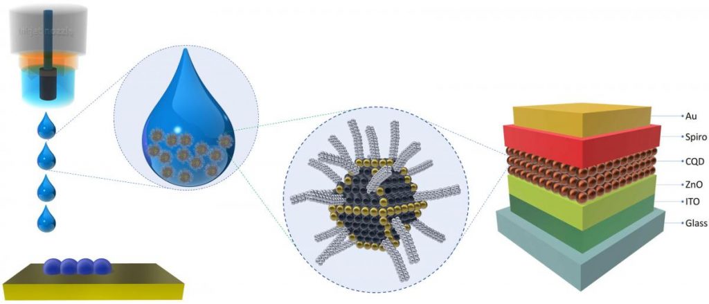
While all this is happening in Kansas, the Econ0mist magazine published a May 12, 2012 article about some important quantum dot optoelectronic developments in Spain (an excellent description for relative beginners is given and, if this area interests you, I’d suggest reading it in full),

Actually converting the wonders of graphene into products has been tough. But Frank Koppens and his colleagues at the Institute of Photonic Sciences in Barcelona think they have found a way to do so. As they describe in Nature Nanotechnology, they believe graphene can be used to make ultra-sensitive, low-cost photodetectors.

A typical photodetector is made of a silicon chip a few millimetres across onto which light is focused by a small lens. Light striking the chip knocks electrons free from some of the silicon atoms, producing a signal that the chip’s electronics convert into a picture or other useful information. …

Silicon photodetectors suffer, though, from a handicap: they are inflexible. Nor are they particularly cheap. And they are not that sensitive. They absorb only 10-20% of the light that falls on to them. For years, therefore, engineers have been on the lookout for a cheap, bendable, sensitive photodetector. …

By itself, graphene is worse than silicon at absorbing light. According to Dr Koppens only 2.7% of the photons falling on it are captured. But he and his colleague Gerasimos Konstantatos have managed to increase this to more than 50% by spraying tiny crystals of lead sulphide onto the surface of the material.

So combining the ability to size quantum dots uniformly with this discovery on how to make graphene more sensitive (and more useful in potential products) with quantum dots suggests some very exciting possibilities including this one mentioned by Dexter Johnson (who’s living in Spain these days) in his May 16, 2012 posting on Nanoclast (on the Institute of Electrical and Electronics Engineers [IEEE] website),

The researchers offer a range of applications for the graphene-and-quantum-dot combination, including digital cameras and sensors.  [emphasis mine] But it seems the researchers seem particularly excited about one application in particular. They expect the material will be used for night-vision technologies in automobiles—an application I have never heard trotted out before in relation to nanotech.

You can get more insights, more precise descriptions if you want to follow up from the Econ0mist article,  and Dexter’s links to more information about the research in his posting.

In my final roundup piece, I received a news release (dated April 24, 2012) about a quantum dot commercialization project at the University of Utah,

One of the biggest challenges for advancing quantum dots is the manufacturing process. Conventional processes are expensive, require high temperatures and produce low yields. However, researchers at the University of Utah believe they have a solution. They recently formed a startup company called Navillum Nanotechnologies, and their efforts are gaining national attention with help from a team of M.B.A. students from the David Eccles School of Business.
The students recently won first place and $100,000 at the regional CU Cleantech New Venture Challenge. The student competition concluded at the University of Colorado in Boulder on Friday, April 20. The student team advances to the national championship, which will be held in June in Washington, D.C. Student teams from six regions will compete for additional prizes and recognition at the prestigious event. Other regional competitions were held at MIT, Cal Tech, the University of Maryland, Clean Energy Trust (Chicago) and Rice University. All the competitions are financed by the U.S. Department of Energy.

The students will be competing in the national Clean Energy Business Plan Competition taking place June 12-13, 2012 in Washington, D.C.  Here are a few more details from the national competition webpage,

Winners of the six regional competitions will represent their home universities and regions as they vie for the honor of presenting the best clean energy business plan before a distinguished panel of expert judges and invited guests from federal agencies, industry, national labs and the venture capital community.

Confirmed Attendees include:

The Honorable Steven Chu
Energy Secretary [US federal government]

Dr. David Danielson
Assistant Secretary, EERE  [US Dept. of Energy, energy efficiency and renewable energy technologies)

Dr. Karina Edmonds
Technology Transfer Coordinator [US Dept. of Energy]

Mr. Todd Park
Chief Technology Officer, White House

Good luck to the students!