Usually, it’s nature which inspires scientists but not this time. Instead, a building in Canberra, Australia has provided the inspiration according to a March 24, 2015 news item on Nanowerk,
Physicists inspired by the radical shape of a Canberra building have created a new type of material which enables scientists to put a perfect bend in light.
The creation of a so-called topological insulator could transform the telecommunications industry’s drive to build an improved computer chip using light.
Leader of the team, Professor Yuri Kivshar from The Australian National University (ANU) said the revolutionary material might also be useful in microscopes, antenna design, and even quantum computers.
“There has been a hunt for similar materials in photonics based on large complicated structures,” said Professor Kivshar, who is the head of the Nonlinear Physics Centre in ANU Research School of Physics and Engineering.
“Instead we used a simple, small-scale zigzag structure to create a prototype of these novel materials with amazing properties.”
The structure was inspired by the Nishi building near ANU, which consists of rows of offset zigzag walls.
Here’s what the building looks like,
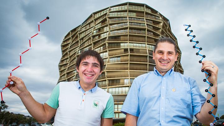
Caption: Alex Slobozhanyuk (L) and Andrey Miroshnichenko with models of their material structures in front of the Nishi building that inspired them.
Credit: Stuart Hay, ANU
A March 24, 2015 Australian National University press release, which originated the news item, goes on to describe topological insulators and what makes this ‘zigzag’ approach so exciting,
Topological insulators have been initially developed for electronics, and the possibility of building an optical counterpart is attracting a lot of attention.
The original zigzag structure of the material was suggested in the team’s earlier collaboration with Dr Alexander Poddubny, from Ioffe Institute in Russia, said PhD student Alexey Slobozhanyuk.
“The zigzag structure creates a coupling throughout the material that prevents light from travelling through its centre,” Mr Slobozhanyuk said.
“Instead light is channelled to the edges of the material, where it becomes completely localised by means of a kind of quantum entanglement known as topological order.”
Fellow researcher Dr Andrew Miroshnichenko said the building inspired the researchers to think of multiple zigzags.
“We had been searching for a new topology and one day I looked at the building and a bell went off in my brain,” said fellow researcher Dr Andrey Miroshnichenko.
“On the edges of such a material the light should travel completely unhindered, surfing around irregularities that would normally scatter the light.
“These materials will allow light to be bent around corners with no loss of signal,” he said.
The team showed that the exceptional attributes of the material are related to its structure, or topology, and not to the molecules it is made from.
“In our experiment we used an array of ceramic spheres, although the initial theoretical model used metallic subwavelength particles,” said Dr Miroshnichenko.
“Even though they are very different materials they gave the same result.”
In contrast with other international groups attempting to create topological insulators with large scale structures, the team used spheres that were smaller than the wavelength of the microwaves in their successful experiments.
Dr Poddubny devised the theory when he realised there was a direct analogy between quantum Kitaev’s model of Majorana fermions and optically coupled subwavelength scatterers.
Mr Slobozhanyuk said the team could control which parts of the material surface the light is channelled to by changing the polarisation of the light.
“This opens possibilities ranging from nanoscale light sources for enhancing microscopes, highly efficient antennas or even quantum computing,” he said.
“The structure couples the two sides of the material, so they could be used as entangled qubits for quantum computing.”
It would be nice to offer a link to a published paper but I cannot find one.
