Tag Archives: Pohang University of Science and Technology (POSTECH)

A pumpkin-shaped molecule for the first real-time methamphetamine and amphetamine sensor

A Sept. 28,2017 news item on Nanowerk announces a portable, inexpensive sensor for drugs (Note: A link has been renewed),

Speed, uppers, chalk, glass, crystal, or whatever you prefer to call them, can be instantly detected from biological fluids with a new portable kit that costs as little as $50. Scientists at the Center for Self-Assembly and Complexity, within the Institute for Basic Science (IBS, South Korea), in collaboration with Pohang University of Science and Technology (POSTECH), have devised the first methamphetamine and amphetamine sensor that can detect minute concentrations of these drugs from a single drop of urine in real-time.

Published in the journal Chem (“Point-of-Use Detection of Amphetamine-Type Stimulants with Host-Molecule-Functionalized Organic Transistors”), this simple and flexible sensor, which can be attached to a wristband and connected to an Android app via Bluetooth, could move drug screening from the labs to the streets.

A Sept. 28 (?), 2017 IBS press release by Letizia Diamante (also on EurekAlert), which originated the news item, expands on the theme,

Easy to synthesize and cheaper than heroin or cocaine, amphetamine-based drugs are the most abused drugs in the world, after cannabis. Conventional drug detection methods require a long time, as the sample must be taken into a lab for the analysis. It also needs experts to run the expensive equipment. The technology reported in this study is instead small, portable, cheap, fast and easy to use.

The idea for this technology came from the IBS chemist HWANG Ilha: “I was watching a TV news report on the usage of illegal drugs, and I thought to check what the chemical structure of methamphetamine looks like.” Soon after, the scientist anticipated that the drug would form a tight complex with a family of hollow pumpkin-shaped molecules, called cucurbituril (CB) members. The team then discovered that cucurbit[7]uril (CB[7])’s empty cavity binds well with amphetamine-based drugs and can be used as the drug recognition unit of a sensor. Cucurbiturils’ hollow chamber has already been studied for various technological uses, but this is the first device application in amphetamine-based drug detection.


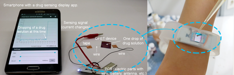
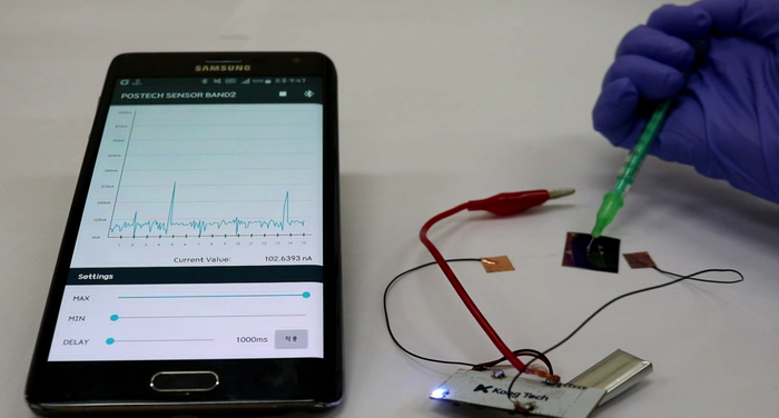
▲ Figure 1: Wireless sensor for amphetamine-based drug detection.The kit is made of an organic field-effect transistor (OFET) device, an electric circuit board with a rechargeable battery and an antenna. The OFET device surface is coated with CB[7], whose function is to bind amphetamine and methamphetamine drugs in solution. The binding event is instantly converted to current, whose magnitude is proportional to the concentration of the drug. The app on the smartphone shows a peak as soon as a drop of urine with the drug is applied to the device. Moreover the entire kit can fit in a handy wristband.


▲ Video 1: The detector in action.
[Click text not image]
As soon as a drop of water with 0.0001 ng/mL (1 pM) of amphetamine is applied to the kit, the app shows a peak in current proportional to the concentration of drug. When the liquid is removed, the current level goes back to baseline, and the sensor can be reused. (Modified from Jang et al, Chem 2017)

Combining a transistor coated with CB[7], flexible materials, rechargeable batteries and a Bluetooth antenna, the research team developed a detector wristband connected to an app. In the presence of the drug, the molecular recognition between CB[7] and the drug molecule triggers an electrical signal which appears as a peak on the smartphone screen.

Current drug detection based on immunoassay or liquid chromatography/mass spectrometry techniques has a detection limit of about 10 ng/mL. On the contrary, the sensitivity of this new sensor is about 0.0001 ng/mL in water and 0.1 ng/mL in urine. Therefore, it is expected that this method will allow the detection of drug molecules in biological fluids, like urine and sweat, for a longer time after drug consumption.


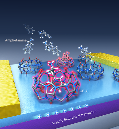
▲ Figure 2: Graphic representation of the drug detection platform.Binding of drug molecules to the hollow cucurbit[7]uril (CB[7])’s cavity changes the current signal flowing in the transistor and therefore can be used as a detection system. The molecular structure of amphetamine and methamphetamine bound to cucurbit[7]uril (CB[7]) was confirmed with X-ray crystallography. Each color indicates a different atom (blue: nitrogen, red: oxygen, gray: carbon, and white: hydrogen). CB[7]’s hydrogen atoms have been omitted for clarity.


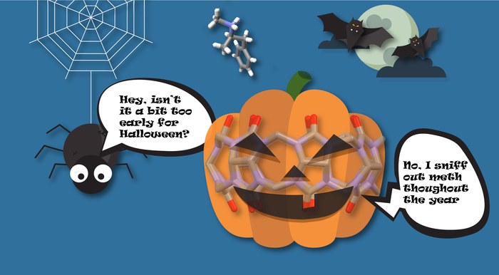
▲ Figure 3: Humorous view of the pumpkin-shaped molecule, cucurbit[7]uril (CB[7]), able to bind and detect amphetamine and methamphetamine molecules.(Credits: Modified from Titusurya – Freepik.com)

“Real time detection of amphetamine drugs on location would bring a big change to society,” explains another corresponding author KIM Kimoon. “In the same way as police can use a breathalyzer to detect alcohol on the spot, we aim to achieve the same with this device.”

False positives cannot be excluded yet, as urine contains a rich mixture of proteins and other metabolites that could affect the reading. Therefore, before commercializing it, clinical trials with drug users’ biological fluids are necessary. The researchers have patented the technology and they will continue to do further research in the near future.s

“Combining basic science with the latest technology, we can expect that this research will also lead to other new sensors, useful for our daily life,” concludes the third corresponding author OH Joon Hak. Indeed, the team is also keen on developing sensors for other kinds of drugs, as well as kits for the detection of dangerous substances, environmental monitoring, healthcare and safety.

Here’s a link to and a citation for the paper,

Point-of-Use Detection of Amphetamine-Type Stimulants with Host-Molecule-Functionalized Organic Transistors by Yoonjung Jang, Moonjeong Jang, Hyoeun Kim, Sang Jin Lee, Eunyeong Jin, Jin Young Koo, In-Chul Hwang, Yonghwi Kim, Young Ho Ko, Ilha Hwang., Joon Hak Oh, Kimoon Kim. Chem (2017). DOI: 10.1016/j.chempr.2017.08.015 Publication stage: In Press Corrected Proof

This paper appears to be behind a paywall.

Making perovskite solar cells more stable and more humidity tolerant

Living in what’s considered a humid environment the news of solar cells that are humidity-resistant caught my attention. From a July 18, 2016 news item on phys.org,

Widely known as one of the cleanest and most renewable energy sources, solar energy is a fast growing alternative to fossil fuels. Among the various types of solar materials, organometal halide perovskite in particular has attracted researchers’ attention thanks to its superior optical and electronic properties. With a dramatic increase in the power conversion efficiency (PCE) from 3% in 2009 to as high as over 22% today [according to my July 13, 2016 posting that efficiency could now be as high as 31%], perovskite solar cells are considered as a promising next-generation energy device; only except that perovskite is weak to water and quickly loses its stability and performance in a damp, humid environment.

A team of Korean researchers led by Taiho Park at Pohang University of Science and Technology (POSTECH), Korea, has found a new method to improve not only the efficiency, but stability and humidity tolerance of perovskite solar cells. Park and his students, Guan-Woo Kim and Gyeongho Kang, designed a hydrophobic conducting polymer that has high hole mobility without the need of additives, which tend to easily absorb moisture in the air. …

A July 18, 2016 Pohang University of Science and Technology (POSTECH) press release on EurekAlert, which originated the news item, provides more information about the work,

Perovskite solar cells in general consist of a transparent electrode, an electron transport layer, perovskite, a hole transport layer, and a metal electrode. The hole transport layer is important because it not only transports holes to the electrode but also prevents perovskite from being directly exposed to air. Spiro-MeOTAD, a conventionally used hole-transport material, needs additives due to its intrinsically low hole mobility. However, Bis(trifluoromethane)sulfonimide lithium salt (LiTFSI), one of the common additives, is prone to suck in moisture in the air. Moreover, Spiro-MeOTAD forms a slightly hydrophilic layer that easily dissolves in water, and thus it cannot work as a moisture barrier itself.

Park’s team focused on an idea of an additive-free (dopant-free) polymeric hole transport layer. They designed and synthesized a hydrophobic conducting polymer by combining benzodithiophene (BDT) and benzothiadiazole (BT). As the new polymer has a face-on orientation, which helps vertical charge transport of holes, the researchers were able to achieve high hole mobility without any additives.

Park and colleagues confirmed that the perovskite solar cells with the new polymer showed high efficiency of 17.3% and dramatically improved stability — the cells retained the high efficiency for over 1400 hours, almost two months, under 75 percent humidity.

“We believe that our findings will bring perovskite one step closer to use and accelerate the commercialization of perovskite solar cells,” commented Taiho Park, a professor with the Department of Chemical Engineering at POSTECH.

Here’s a link to and a citation for the paper,

Dopant-free polymeric hole transport materials for highly efficient and stable perovskite solar cells by Guan-Woo Kim, Gyeongho Kang, Jinseck Kim, Gang-Young Lee, Hong Il Kim, Limok Pyeon, Jaechol Lee, and Taiho Park. Energy Environ. Sci., 2016,9, 2326-2333 DOI: 10.1039/C6EE00709K First published online 28 Apr 2016

I wonder if the press release was originally written in April 2016? That would explain the difference in efficiency I noted earlier in the press release. Getting back to the paper, it is open access with three different means of accessing the material from the publisher, the Royal Society of Chemistry.

Making lab-on-a-chip devices more accurate

An April 4, 2016 news item on phys.org announces research that will improve control and manipulation of the fluids in a lab-on-a-chip,

Lab-on-a-chip designates devices that integrate various biochemical functions on a fingernail-sized chip to enable quick and compact biological analysis or medical diagnosis by processing a small volume of biological samples, such as a drop of blood. To operate various functions on a lab-on-a-chip device, the key technology is the precise and rapid manipulation of fluid on a micro-scale.

A March 31, 2016 Pohang University of Science and Technology (POSTECH; South Korea) press release (also on EurekAlert), which originated the news item, expands on the theme,

In microfluidic devices, very small and trivial variables can frequently cause a large amount of errors. Up until now, Proportional-Integral-Derivative (PID) controller has normally been used for the manipulation of fluids in microfluidic chips. To apply the PID controller, a tedious gain-tuning process is required but the gain-tuning is a difficult process for people who are unfamiliar with control theory. Especially, in the case of controlling multiple flows, the process is extremely convoluted and frustrating.

The developed control algorithm can improve accuracy and stability of flow regulation in a microfluidic network without requiring any tuning process. With this algorithm, microfluidic flows in multiple channels can be controlled in simultaneous and independent way. The team expects that this algorithm has the potential for many applications of lab-on-a-chip devices. For example, cell culture or biological analysis, which are conducted in biology laboratories, can be performed on a microfluidic chip. Physical and chemical responses can be analyzed in the subdivided levels.

Here’s a link to and a citation for the paper,

Tuning-free controller to accurately regulate flow rates in a microfluidic network by Young Jin Heo, Junsu Kang, Min Jun Kim, & Wan Kyun Chung. Scientific Reports 6, Article number: 23273 (2016) doi:10.1038/srep23273 Published online: 18 March 2016

This is an open access paper.

Korean researchers fabricate cross-shaped memristors

I’ve been a bit late getting this Korean research concerning memristors into a posting. A Jan. 30, 2016 news item on Nanotechnology Now announces a new means of fabricating memristors,

Along with the fast development of modern information technology, charge-based memories, such as DRAM and flash memory, are being aggressively scaled down to meet the current trend of small size devices. A memory device with high density, faster speed, and low power consumption is desired to satisfy Moore’s law in the next few decades. Among the candidates of next-generation memory devices, cross-bar-shaped non-volatile resistive memory (memristor) is one of the most attractive solutions for its non-volatility, faster access speed, ultra-high density and easier fabrication process.

Conventional memristors are usually fabricated through conventional optical, imprint, and e-beam lithographic approaches. However, to meet Moore’s law, the assembly of memristors comprised of 1-dimensional (1D) nanowires must be demonstrated to achieve cell dimensions beyond limit of state-of-art lithographic techniques, thus allowing one to fully exploit the scaling potential of high density memory array.

Prof. Tae-Woo Lee (Dept. of Materials Science and Engineering) and his research team have developed a rapid printing technology for high density and scalable memristor array composed of cross-bar-shaped metal nanowires. The research team, which consists of Prof. Tae-Woo Lee, research professor Wentao Xu, and doctoral student Yeongjun Lee at POSTECH [Pohang University of Science and Technology], Korea, published their findings in Advanced Materials.

A Jan. 28, 2016 POSTECH news release, which originated the news item, expands on the theme,

They applied an emerging technique, electrohydrohynamic nanowire printing (e-NW printing), which directly prints highly-aligned nanowire array on a large scale into the fabrication of microminiature memristors, with cross-bar-shaped conductive Cu nanowires jointed with a nanometer-scale CuxO layer. The metal-oxide-metal structure resistive memory device exhibited excellent electrical performance with reproducible resistive switching behavior.

This simple and fast fabrication process avoids conventional vacuum techniques to significantly reduce the industrial-production cost and time. This method paved the way to the future down-scaling of electronic circuits, since 1D conductors represent a logical way to extreme scaling of data processing devices in the single-digit nanometer scale.

They also succeeded in printing memristor array with various shapes, such as parallel lines with adjustable pitch, grids, and waves which can offer a future stretchable memory for integration into textile to serve as a basic building block for smart fabrics and wearable electronics.

“This technology reduces lead time and cost remarkably compared with existing manufacturing methods of cross-bar-shaped nanowire memory and simplifies its method of construction,” said Prof. Lee. “In particular, this technology will be used as a source technology to realize smart fabric, wearable computers, and textile electronic devices.”

Here’s a link to and a citation for the paper,

[Nanowires:] Simple, Inexpensive, and Rapid Approach to Fabricate Cross-Shaped Memristors Using an Inorganic-Nanowire-Digital-Alignment Technique and a One-Step Reduction Process by Wentao Xu, Yeongjun Lee, Sung-Yong Min, Cheolmin Park, andTae-Woo Lee. Advanced Materials Volume 28, Issue 3 January 20, 2016 Page 591  DOI: 10.1002/adma.201503153 Article first published online: 20 NOV 2015

© 2015 WILEY-VCH Verlag GmbH & Co. KGaA, Weinheim

This paper is behind a paywall.